

Samsung SGH-R200 Troubleshooting
5. Flow Chart of Troubleshooting
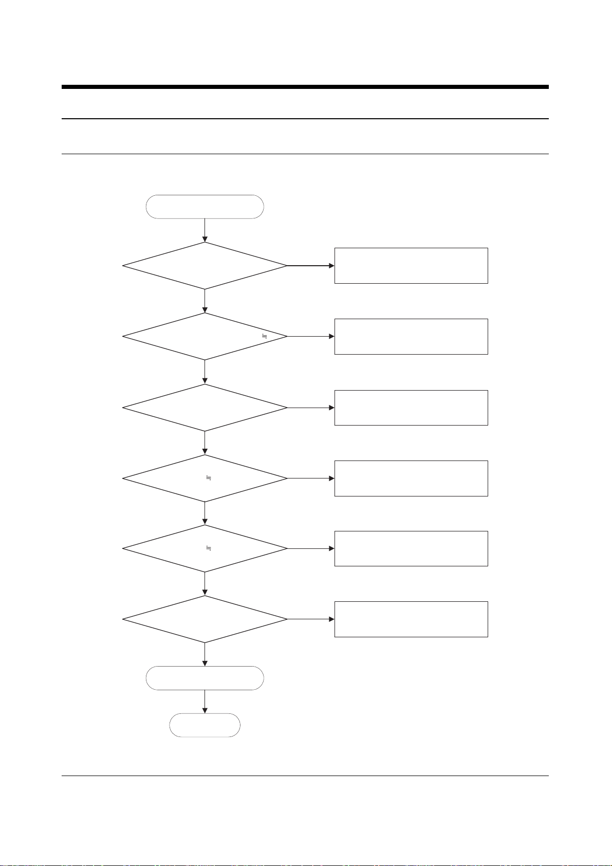
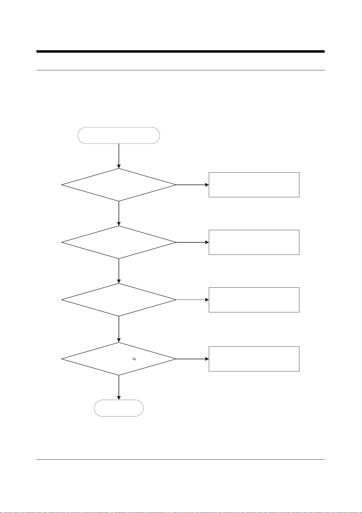
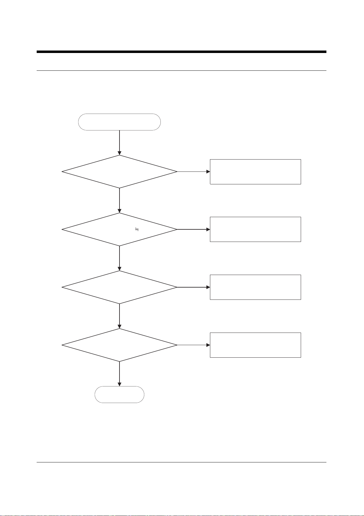
5-1 Power ON
Flow Chart of Troubleshooting and Circuit Diagrams 5-1
'POWER ON'does not work
Charge the Battery
Check the Battery Voltage
is more than 3.2V
No
Yes
Yes
Replace Keypad
When the "END" key is
pressed, the voltage of "D109 pin1"
3.6V?
No
Yes
U101 pin 2,3 > 3.2V Check the circuit related to U101
No
END
U103 pin 1 3.0 V ? Check the circuit related to U103
No
Yes
Check the initial operation
U103 pin2 3.0 V ? Check U103 and related circuit
No
Yes
Check for the clock signal at R320
Check the clock generation circuit
(related to U305 and Q301)
No
Yes
Yes
Flow Chart of Troubleshooting and Circuit Diagrams5-2
100UF
+VBATT
POWER
RTC_3V3
DCVOLT
RTC_3V3
12345
D109
UMN1
100K
R116
R112
10K
10K
2
3
4
5
R119
U106
UMC5NTL
1
R120
100K
C141
100NF
R117
10K
DCIN
BB_PWR
ON_OFF
10K
R121
One Point Contact
1UF
C122
1UF
C221
SIMVCC
C119
C131
10NF
C220
C218
10NF
NC
C222
1UF
AVCC
10NF
C117
100UF
C120
C217
100NF
2
3
ON/OFF
VIN
1
VOUT
5
MCL4154
D110
U105
LP2985AIM5-3.3
BYPASS
4
GND
10UF/6.3V
C133
100PF
C138
C118
10UF/6.3V
C137
27PF
VCC
10UF/6.3V
C140
C126
NC
LP2985AIM5-3.3
4BYPASS
GND2ON/OFF
3
VIN
1
5
VOUT
1K
R106
U102
RB414
C105
NC
C219
1UF
BAT101
10NF
C123
C121
10UF/6.3V
10NF
C128
VOUT1
VOUT2
2
3
VOUT3
100NF
C139
R5320G003A-TP
CE1
7
6
CE2
CE3
5
GND
4
8
VDD
1
R107
U103
1K
R101
100K
D23D2
5
ON/OFF
R1,C1
61
R2
4
S2
SI3865DV
U101
2
C134
10UF/6.3V
10NF
C136
VOUT
ALERT_VCC
RTC_VCC
Flow Chart of Troubleshooting and Circuit Diagrams 5-3
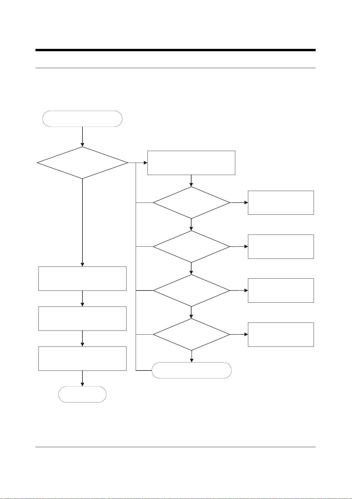
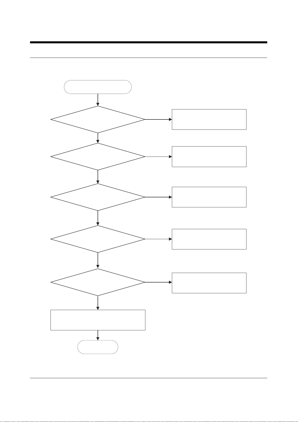
5-2 Initial
Initial Failure
After power on,
check and repair the important
signals of U110 as follows
END
No
Downloading SW is OK ?
(Is CSROM signal OK ?)
The node
between R126 and C145
= "H" (RST)
No
Check the circuit
related to reset
R137 = "H" (BOOT)
No
Resolder R137
Yes
R136 = "H" (MSIZE)
No
Resolder R136
Yes
R128 = "L" (EXTPROC)
No
Resolder R138
Yes
Replace PBA
Check all the other connection
by Test S/W
Check the circuit around LCD
Check the circuit
around U113(EEPROM)
and data stored in it
Yes
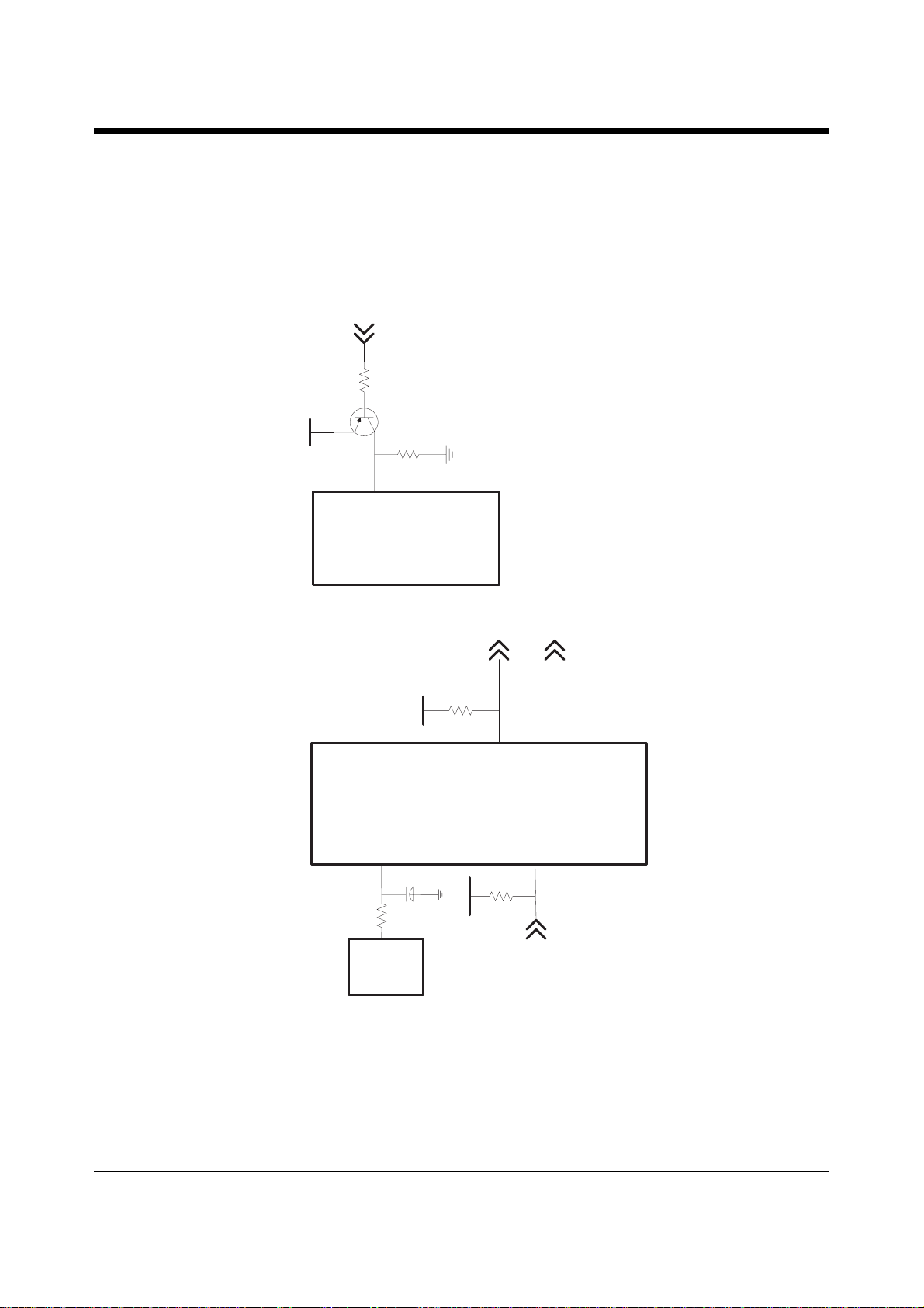
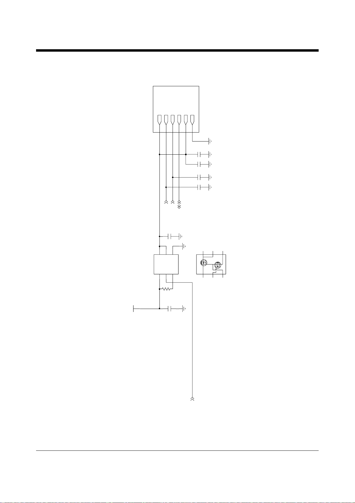
Flow Chart of Troubleshooting and Circuit Diagrams5-4
U110
U107
U109
VCC
VCC
R126
C145
R137
R136
R147
VCC
MSIZE
SIMPWDN_BOOT
F_WP
F_WP
_WP/ACC
SYSRST
GPIO3
GPIO4
GPO2
Q106
R128
CSROM _CE
Flow Chart of Troubleshooting and Circuit Diagrams 5-5
5-3 Charging Part
Abnormal charging part
Replace T ACheck the J105 pin 17,18 = 5.0 V ?
No
Yes
Yes
Check the U104 pin 3 = 5.0 V ? Resolder C135
Yes
No
R113(CHG_ON side) = "L" ? Resolder R113
Yes
No
Resolder components around
U104
Check the U104 pin 5 4.2V ?
END
Yes
No
Flow Chart of Troubleshooting and Circuit Diagrams5-6
LTC1734ES6-4.2#TR
DRIVE
6
U104
C127
CHG_ON
+VBATT
DCVOLT
I_CHARGE
BAT_VOLT
R110
100K,1%
GND
2
1
ISENSE
PROG
43
VCC
5
VSENSE
C135
10UF
10V
R113
2.2K,1%
82K,1%
R111
Q101
ZXT13P20DE6
3
1256
4
C125
100NF
10UF
6.3V
Flow Chart of Troubleshooting and Circuit Diagrams 5-7
5-4 Sim Part
Q102 pin5 = "H" ?
Replace Q102 or
Replace PBA
END
Yes
No
Check the circuit around U113
(Serial EEPROM) and data stored in it
Yes
Phone can't access SIM card
Yes
Q102 pin 2, 3 = 3.0 V ?
Replace Q102 or
Resolder C132
Yes
No
After Power ON,
Check SIMCLK Signal on CN102 pin 3
in a few second
After SIM card insert,
CN102 pin 2 = "H(SIMRST) ?
Resoldering C193 or
Replace PBA
Resoldering C192 or
Replace PBA
Yes
No
No
Q102 pin4 = 3.0 V ?
Yes
No
Check the circuit around U103
Flow Chart of Troubleshooting and Circuit Diagrams5-8
465
3
2
1
SIM CONNECTOR
J104
NC
C216C215
NC
SIMVCC
100PF
C193
8
C192
100PF
6
J104-5 1-338063-97J104-6 1-338063-9
2
1-338063-9J104-3
3
J104-4 1-338063-9
J104-1 1-338063-9
1
1-338063-9J104-2
6
R1,C1
1
R2
V.C1-1
2
V.C1-2
3
VIN,R1
4
FDG6323L
Q102
ON/OFF
5
10NF
C132
C124
1UF
10K
R108
SIMPWREN
SIMRST
SIMDATA
SIMCLK
Flow Chart of Troubleshooting and Circuit Diagrams 5-9
5-5 Microphone Part
Microphone does not work
Resoler J102J102 pin 4, 5 = short?
U103 pin 2 (AVCC3.0) 3.0V?
Check the circuit
from U110 to MIC101
Check the circuit related to U103
END
Resolder the
R146,R157,R150,R155,
C163,C161,C164
Yes
No
Yes
Yes
Yes
No
No
Check the tension of MIC Module Replace the Mic or Mic Holder
No
Yes
 Loading...