

Samsung SGH-P930 Service Manual

GSM TELEPHONE
SGH-P930
GSM TELEPHONE
CONTENTS
1. Specification
2. Exploded View and Parts list
3. Chart of Troubleshooting
4. Array course control
5. Block Diagrams
6. PCB Diagrams
7. MAIN Electrical Parts List
8. Reference data
9. Safety Precautions
10. Product Function

Contents
1. Specification
1-1. GSM/WCDMA General Specification ........................................................................1-1
1-2. GSM TX power class ...............................................................................................1-2
2. Exploded View and Parts list
2-1. Cellular phone Exploded View ..................................................................................2-1
2-2. Cellular phone Parts list ............................................................................................2-2
2-3. Disassembly ...............................................................................................................2-4
2-4. Assembly ....................................................................................................................2-7
3. Chart of Troubleshooting
3-1. Baseband ............................................................................................................3-1
3-1-1. Power ON ...................................................................................................3-1
3-1-2. System Initial ..............................................................................................3-2
3-1-3. SIM Part .....................................................................................................3-5
3-1-4. Charging Part .............................................................................................3-7
3-1-5. Microphone Part .......................................................................................3-10
3-1-6. Speaker Part ............................................................................................3-12
3-1-7. Receiver Part ...........................................................................................3-15
3-1-8. Camera Part .............................................................................................3-17
3-1-9. VGA CAMERA Part .................................................................................3-20
3-1-10. LCD Part ..................................................................................................3-22
3-2. RF ......................................................................................................................3-25
3-2-1. EGSM Receiver .......................................................................................3-25
3-2-2. EGSM Transmitter ....................................................................................3-26
3-2-3. DCS Receiver ...........................................................................................3-27
3-2-4. DCS Transmitter .......................................................................................3-28
3-2-5. PCS Receiver ...........................................................................................3-29
3-2-6. PCS Transmitter .......................................................................................3-30
3-2-7. UMTS Receiver ........................................................................................3-34
3-2-8. UMTS Transmitter ....................................................................................3-35
3-2-9. BLUETOOTH ............................................................................................3-38
3-2-10. DVB-H .......................................................................................................3-40

Contents
4. Array course control
4-1. Downloading Binary Files ......................................................................................4-2
4-2. Pre-requsite for Downloading ................................................................................4-2
4-3. S/W Downloader Program .....................................................................................4-3
5. Block Diagrams
6. PCB Diagrams
7. MAIN Electrical Parts List
8. Reference data
8-1. Reference Abbreviate ..............................................................................................8-1
9. Safety Precautions
9-1. Repair Precaution ......................................................................................................9-1
9-2. ESD(Electrostaically Sensitive Devices) Precaution ................................................9-2
10. Product Function

1. Specification
1-1. GSM/WCDMA General Specification
EGSM 900
Phase 2
Freq. Band[MHz]
Uplink/Downlink
ARFCN range
Tx/Rx s p a c i n g 45 MHz 95 MHz 80 MHz 190 MHz
Mod. Bit rate/
Bit Period
Time Slot
Period/Frame
Period
Modulation 0.3 GMSK 0.3 GMSK 0.3 GMSK
880~915
925~960
0~124 &
975~1023
270.833 kbps
3.692 us
576.9 us
4.615 ms
DCS1800
Phase 1
1710~1785
1805~1880
512~885 512~810 10562~10838
270.833 kbps
3.692 us
576.9 us
4.615 ms
PCS1900 WCDMA
1850~1910
1930~1990
270.833 kbps
3.692 us
576.9 us
4.615 ms
1920~1980
2110~2170
3.84 Mcps/s
10 ms
UL:2BPSk
DL:QPSK
MS Power 33dBm~5dBm 30dBm~0dBm 30dBm~0dBm
Power C l a s s 5 pcl ~ 19 pcl 0 pcl ~ 15 pcl 0 pcl ~ 15 pcl CLASS3
Sensitivity -102 dBm -100 dBm -100 dBm -106.7 dBm
TDMA Mux 8 8 8 -
Cell Radius 35 Km 2 Km - -
MAX:24(+1,-3) dBm
MIN:<-50 dBm
1-1
SAMSUNG Proprietary-Contents may change without notice
This Document can not be used without Samsung's authorization
Specification
1-2. GSM TX power class
TX Power
control level
EGSM900
533±2dBm
631±2dBm
729±2dBm
827±2dBm
925±2dBm
10 23±2 dBm
11 21±2 dBm
TX Power
DCS1800
control level
030±3dBm
128±3dBm
226±3dBm
324±3dBm
422±3dBm
520±3dBm
618±3dBm
TX Power
control level
PCS1900
030±3dBm
128±3dBm
226±3dBm
324±3dBm
422±3dBm
520±3dBm
618±3dBm
12 19±2 dBm
13 17±2 dBm
14 15±2 dBm
15 13±2 dBm
16 11±3 dBm
17 9± 3dBm
18 7±3 dBm
19 5±3 dBm
716±3dBm
814±3dBm
912±4dBm
10 10±4 dBm
11 8±4 dBm
12 6±4 dBm
13 4±4 dBm
14 2±5 dBm
716±3dBm
814±3dBm
912±4dBm
10 10±4 dBm
11 8±4 dBm
12 6±4 dBm
13 4±4 dBm
14 2±5 dBm
15 0±5 dBm
1-2
15 0±5 dBm
SAMSUNG Proprietary-Contents may change without notice
This Document can not be used without Samsung's authorization
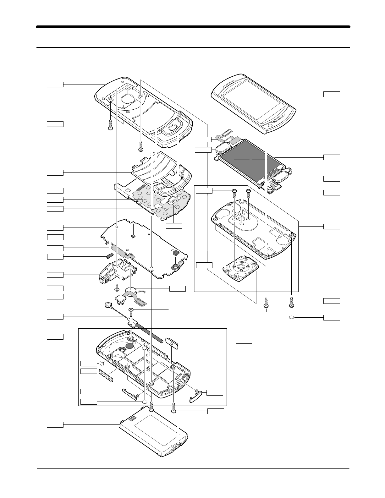
2. Exploded View and Parts List
2-1. Cellular phone Exploded View
QFR01
QCR12
QFU01
QME03
QSP01
QLC01
QKP01
QKP02
QME01
QSH01
QMP01
QAN11
QVK01
QAN05
QAN02
QCR06
QCA01
QAN01
QRE01
QJK03
QMO01
QCR04
QCR32
QHI01
QSP01
QCA02
QFL01
QCR26
QSC14
QCK01
QBA01
QRF01
QVO01
QSD01
QRF02
QIF01
QCR06
2-1
SAMSUNG Proprietary-Contents may change without notice
This Document can not be used without Samsung's authorization
Exploded View and Parts List
2-2. Cellular phone Parts list
Design LOC Discription SEC CODE
QAN01
QAN02
QAN05
QAN11
QBA01
QCA01
QCA02
QCK01
QCR04
QCR06
QCR06
QCR12
QCR26
QFR01
QFU01
QJK03
QKP01
QKP02
QLC01
QME01
QME03
QMO01
QMP01
QRF01
QRF02
QSC14
QSH01
QSP01
QVK01
QRE01
QFL01
ASSY-CUSHION-CUSHION RUBBER IN GH98-01077A
ANTENNA-SGHP930 DVB-H GH42-00999A
INTENNA-SGHP930 GH42-00994A
ASSY MEC-INTENNA CONTACT GH75-08168A
BATTERY-950MAH,BLK,ENG,M GH43-02649A
UNIT-SGHP930 2M CAMERA(REC) GH59-03680A
UNIT-SGHP930 VGA CAMERA(SELF) GH59-03684A
PMO-CAMERA KEY GH72-34749A
SCREW-MACHINE 6001-001479
SCREW-MACHINE 6001-001155
SCREW-MACHINE 6001-001155
SCREW-MACHINE 6001-001530
SCREW-MACHINE 6001-001850
ASSY COVER-FRONT GH98-02469A
ASSY COVER-SWING UPPER GH98-02467A
ASSY KEY-JOG GH98-02470A
ASSY KEYPAD-MAIN(BLK/OPEN) GH98-02473A
ASSY KEYPAD-SUB(BLK/OPEN) GH98-02474A
LCD-MODULE SGHP930 GH07-00997A
UNIT-SGHP930 KEY PBA GH59-03683A
UNIT-SGHP930 CON TO CON GH59-03669A
MOTOR DC-SPHM500 GH31-00242A
PBA MAIN-SGHP930 GH92-03094A
PMO-COVER RF GH72-34850A
MPR-TAPE SHEET RF GH74-28179A
MPR-TAPE SHEET LOWER SCREW GH74-28163A
ASSY COVER-SHIELD CAN GH98-02916A
SPEAKER 3001-002059
UNIT-SGHP930 VOLUME KEY GH59-03685A
ASSY CASE-REAR GH98-02471A
QSD01 PMO-COVER SD GH72-34747A
QIF01 PMO-COVER IF GH72-34748A
QVO01 PMO-VOLUME KEY V2 GH72-34751A
ASSY COVER-SWING LOWER GH98-02468A
QCR32 SCREW-MACHINE 6001-001700
QHI01 ASSY HINGE GH98-02472A
2-2
SAMSUNG Proprietary-Contents may change without notice
This Document can not be used without Samsung's authorization

Exploded View and Parts List
Discirption SEC CODE
BAG PE 6902-000634
CBF INTERFACE-DATA LINK CABLE GH39-00444A
ADAPTOR-SGHE690,BLK,EU,A_TYPE GH44-01361A
S/W CD-SAMSUNG PC STUDIO 3.0 GH46-00314A
UNIT-EARPHONE(BLK) GH59-02499A
LABEL(P)-WATER SOAK GH68-02026A
LABEL(P)-WATER SOAK GH68-02026A
MANUAL USERS-TIM ITALIAN GH68-12567A
LABEL(R)-MAIN_TIM GH68-13072F
BOX(P)-UNIT MAIN(SEA_2) GH69-04699K
CUSHION-CASE TA2 MA2 GH69-04700A
MPR-BOHO VINYL IF GH74-13606A
MPR-BOHO VINYL LCD CONN GH74-15350A
MPR-SPONGE LOWER B GH74-28150A
MPR-SPONGE MIC GH74-28154A
MPR-TAPE LEAK L GH74-28552A
MPR-TAPE LEAK R GH74-28553A
MPR-INSU TAPE GH74-29175A
MPR-INSU TAPE GH74-29176A
MPR-INSU TAPE GH74-29178A
MPR-VINYL BOHO UPPER GH74-29188A
MPR-GASK TAPE GH74-29300A
MPR-GASK TAPE GH74-29328A
MPR-VINYL BOHO VIEW GH74-29331A
MPR-GASK TAPE GH74-29411A
MPR-GASK TAPE SCREW GH74-29609A
AS-IC-MCP UMTS GH81-06104A
2-3
SAMSUNG Proprietary-Contents may change without notice
This Document can not be used without Samsung's authorization

Exploded View and Parts List
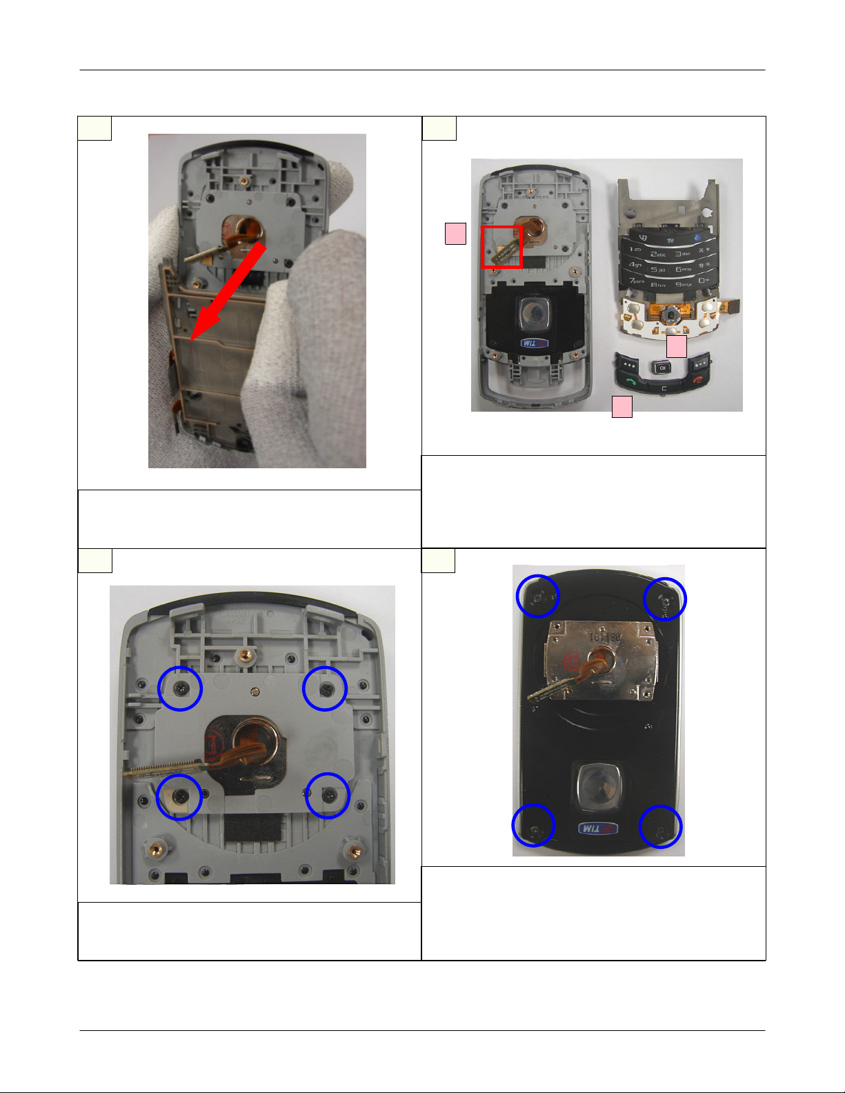
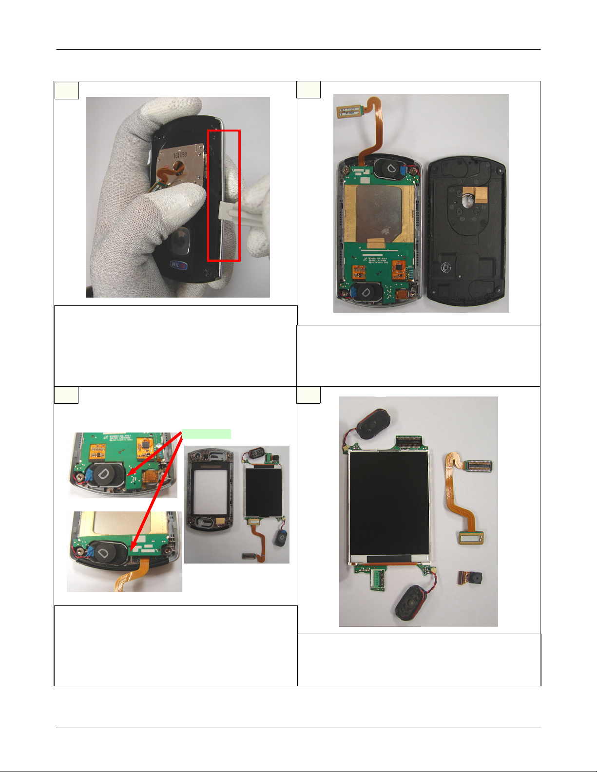
5-3. Disassembly
1
1) Drain REAR Screw 4 Points.
2) Open IF COVER
※
caution
1) take care that it does not happen scratch
2
②
③
①
1) First dissolution REAR's lower column department
locker uses a decomposition tool and dissolution
such as picture.
※
caution
1) take care that it does not happen scratch
③
②
①
1) Separate LCD, CAMERA, KEY connector.
2) Separate VOL KEY FPCB using tweezers.
3) Drain SCREW that is contracted to PBA.
※
caution
1) When separate LCD, CAMERA, KEY
CONNECTOR FPCB and VOLUME KEY FPCB,
take care that FPCB may not be damaged.
43
MOTOR
decomposition
groove
1) Separate PBA in FRONT.
2) Using MOTOR decomposition groove Separate
MOTOR in Braket.
※
caution
1) When separate, take care that CAMERA
CONNECTOR FPCB and MOTOR WIRE does
not damaged
2-4
SAMSUNG Proprietary-Contents may change without notice
This Document can not be used without Samsung's authorization
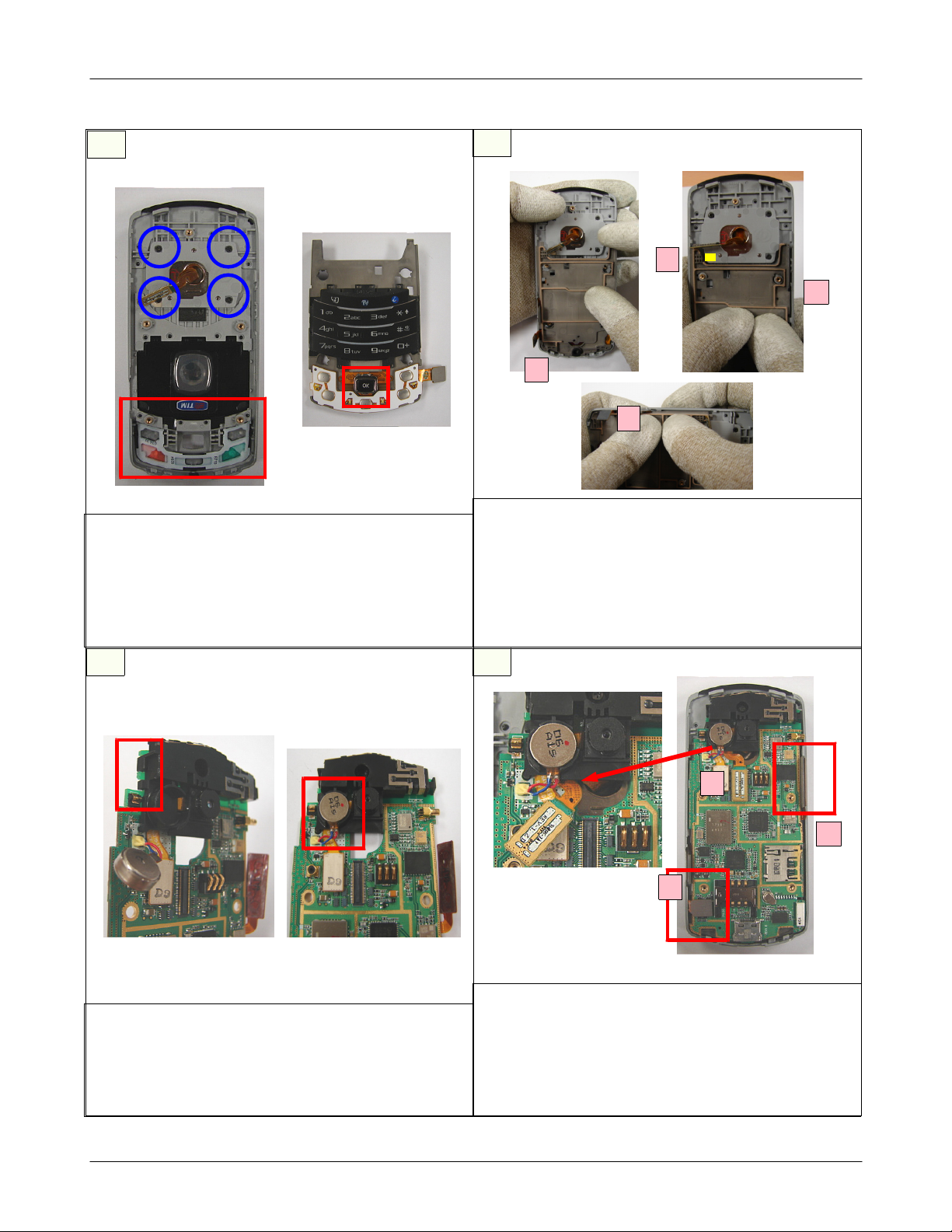
Exploded View and Parts List
5
1) Separate KEY PBA in FRONT.
※
caution
1) take care that it does not happen scratch
6
③
①
②
1) Separate JOG KEY in KEY PBA.
2) Separate SUB KEY in FRONT.
3) Separate challenge TAPE in FRONT.
※
caution
1) take care that it does not happen scratch
1) Drain FRONT SCREW 4 POINTs.
※
caution
1) take care that it does not happen scratch
87
1) Separate SWING SCREW 4 POINTs by using
tweezers
2) Drain LOWER SCREW 4 POINTs.
※
caution
1) take care that it does not happen scratch
2-5
SAMSUNG Proprietary-Contents may change without notice
This Document can not be used without Samsung's authorization
Exploded View and Parts List
9
1) First separate LOWER's left side hook uses a
decomposition tool and disjoints remainder hooks.
2 )Right and left side hook each 3 EAs,
up and down hook each 1 EA
※
caution
1) take care that it does not happen scratch
10
1) Separate LOWER and UPPER.
※
caution
1) Take care so that LCD FPCB may not be
damaged.
11
SPEAKER
1) Sepatate both SPEAKER using separates
decomposition groove.
2) Separate LCD ASS' Y in UPPER.
※
caution
1) Take care so that SPEAKER WIRE may not
separate.
12
1) Separate VGA CAMERA and LCD FPCB in LCD
ASS' Y
※
caution
1) Judge the sepate items are good or not.
2-6
SAMSUNG Proprietary-Contents may change without notice
This Document can not be used without Samsung's authorization

5-4. Assembly
Exploded View and Parts List
1
1) Contract VGA CAMERA and LCD FPCB to
LCD.
2) Attach the Insulation TAPE on the VGA
CAMERA CONNECTOR top portion
※
caution
1) Take care damage when insert CAMERA FPCB.
2
1) Insert LCD ASS'y to UPPER.
2) Insert Both SPEAKER like a picture
※
caution
1) When conclude SPEAKER WIRE, take care
interference
①
1) Contack SWING UPPER and LOWER by
method such as picture
※
caution
1) take care that it does not happen scratch
2) take care that LCD FPCB does not interference
to the body
②
③
④
43
1) Contract SCREW 4 POINTs.
2) Attach SCREW stack 4 POINTs.
※
caution
1) take care that it does not happen scratch
2-7
SAMSUNG Proprietary-Contents may change without notice
This Document can not be used without Samsung's authorization
Exploded View and Parts List
5
1) Contract SUB KEYPAD to FRONT with picture.
2) Contract SCREW 4 POINTs.
3) Combine JOG KEY to KEY PBA.
※
caution
1) take care that it does not happen scratch
2)ObservetoJOGKEYwrongcontract
6
④
②
①
③
1) Contract KEY PBA ASS' Y to FRONT.
2) Attach challenge TAPE on FRONT left side
lower column.
※
caution
1) take care that it does not happen scratch
2) KEY PAD is lacking accordantly with FRONT.
1) Combine PBA and Intenna Braket.
2) Combine MOTOR in Intenna department.
※
caution
1) Take care that CAMERA FPCB and MOTOR
WIRE does not go damaged
87
①
②
③
1) Contract LCD CONNECTOR after combine PBA
to FRONT.
2) Attaches VOL KEY and contracts KEY
CONNECTOR
※
caution
1) take care that it does not happen scratch
2-8
SAMSUNG Proprietary-Contents may change without notice
This Document can not be used without Samsung's authorization
Exploded View and Parts List
9
①
②
LOCKER
③
1) Contract REAR to FRONT ASS' Y In order such
as picture
※
caution
1) take care that it does not happen scratch
③
10
1) Contract to SCREW 4 POINTs.
※
caution
1) take care that it does not happen scratch
2-9
SAMSUNG Proprietary-Contents may change without notice
This Document can not be used without Samsung's authorization
3. Chart of Troubleshooting
3-1. Baseband
3-1-1. Power ON
'Power ON' Does not work
Check the current consumption
Current consumption
≥
100mA ?
YES
Voltage≥3.3V ?
YES
R509≥2.4V ?
YES
Check the Clock at
OSC500=32kHz
YES
Check U500
C511(MSMP_2.6V)=2.6V?
C513(MSMC_1.375)=1.375V?
C512(MSMA_2.6V)=2.6V?
C514(MSME_1.8V)=1.8V?
NO
NO
NO
NO
NO
Down load again
Charge the Battery
Check the PMIC related to
PS_HOLD
Resolder OSC 500
Check the PMIC(U500)
YES
Check the clock at
TCX800=19.2MHz
YES
Check the Initial operation
YES
END
SAMSUNG Proprietary-Contents may change without notice
This Document can not be used without Samsung's authorization
3-1
NO
check the clock generation
circuit(TCX800)
Flow Chart of Troubleshooting and Circuit Diagrams
3-1-2. System Initial
Initial Failure
The pin #9 of U500
" Low --> High" ?
YES
Check the Sleep X-tal signal's at C519 ?
YES
Check the clock signal's
at R504
YES
LCD Display OK ?
YES
Sound operation OK ?
NO
NO
NO
NO
NO
Check the U500
Check the OSC500
Check the clock
generation circuit
(related to
U501 and TCX800
Check the LCD part
Check the Audio part
YES
END
3-2
SAMSUNG Proprietary-Contents may change without notice
This Document can not be used without Samsung's authorization
Flow Chart of Troubleshooting and Circuit Diagrams
PS_HOLD
38
RUIM_CLK26RUIM_IO34RUIM_M_CLK
VDD_MSME
35
Q501
2
RESET_IN
C522
USIM_M_CLK
USIM_DATA
VDD_MSMC
VDD_PA
29
33
ON_SW
1
3
R507 100
D-
USIM_M_DATA
(0603)
57
24
66
9
RUIM_M_IO30RUIM_M_RST
KPDPWR_N
USB_D_M20USB_D_P18USB_ID
PON_RESET_N
PS_HOLD
CBL0PWR_N68CBL1PWR_N
SPKR_OUT_M
SPKR_OUT_P
SPKR_IN_M
SPKR_IN_P
VDD_SPKR
SPKR_BYP
77
75
74
78
79
VBAT
ZD501
R508
JIG_ON
(0603)
USIM_M_RESET
USIM_RESET
PM_SBDT
USIM_CLK
PM_INT_N
PM_SBCK
PM_SBST
43
49
51
40
59
MSM_INT_N
RUIM_RST
SBCK
SBDT47SBST
5
8
G
N
D
6
8
N
C
7
8
N
C
VDD_WLAN
VDD_RUIM
VDD_MAIN
VDD_MSM
VDD_ANA
VDD_RF
71
41
65
54
83
52
C525
C526
C523
C527
C524
BAT500
POS
NEG
1
2
C507
R506
VBAT
C509
D+
USB_VMO
USB_VPO
11
19
USB_SE0
USB_OE_N
17
13
USB_DAT
USB_OE_N
C520
PMIC3_REF
80
REF_OUT
21
OSC500
C519
SLEEP_XTAL_IN
AMUX_OUT
TCXO_OUT
TCXO_EN
BAT_VF
TCXO
R504
C508
55
53
45
70
82
TCXO_EN
TCXO_IN58TCXO_OUT
SLEEP_CLK
AMUX_IN272AMUX_OUT
AMUX_IN1
46
1
VBACKUP48VBAT6VCHG
ADC_BYP
XTAL_IN44XTAL_OUT
7
BAT_FET_N
TA503
C504
C500
R502
16
60
15
3
2
4
ISNS_M5ISNS_P
USB_VBUS
VCOIN
USB_CTL_N
CHG_CTL_N
VBAT
C501
R501
USB_VCC
U500
VREG_RFRX169VREG_RFRX2
VREG_MSMA
FLSH_DRV_N
KPD_DRV_N
LCD_DRV_N
GP1_DRV_N
VIB_DRV_N
REF_GND62REF_ISET
25
23
22
76
21
8
C521
VREG_WLAN
VREG_TCXO
VREG_SYNT
VREG_RFTX
REF_BYP
81
84
64
67
63
61
73
R505
VREG_MSMC
VREG_MSME
VREG_MSMP
VREG_RUIM
VSW_MSMC
VSW_MSME
VREG_MMC
VREG_USB
VREG_PA
VREG_5V
VSW_PA
VSW_5V
42
10
39
56
50
C506
14
31
32
36
28
12
37
27
C502 C503
L501
L500
C513
C531
C528
C529
C530
C532
L504
L505
C517
RFRX1_2.85V RFRX_2.85V
C518
C514
C515
C510
OSC_2.85VRFTX_2.85V
TCXO_2.85V
C511
C512
C516
R514
R515
MSMC_1.375V
R513TA502
MSME_1.8V
R512
MICBIAS_2.85V
USIM_2.85V
MSMP_2.6V
MSMA_2.6V
BT_3.0V
3-3
SAMSUNG Proprietary-Contents may change without notice
This Document can not be used without Samsung's authorization

Flow Chart of Troubleshooting and Circuit Diagrams
3-4
SAMSUNG Proprietary-Contents may change without notice
This Document can not be used without Samsung's authorization
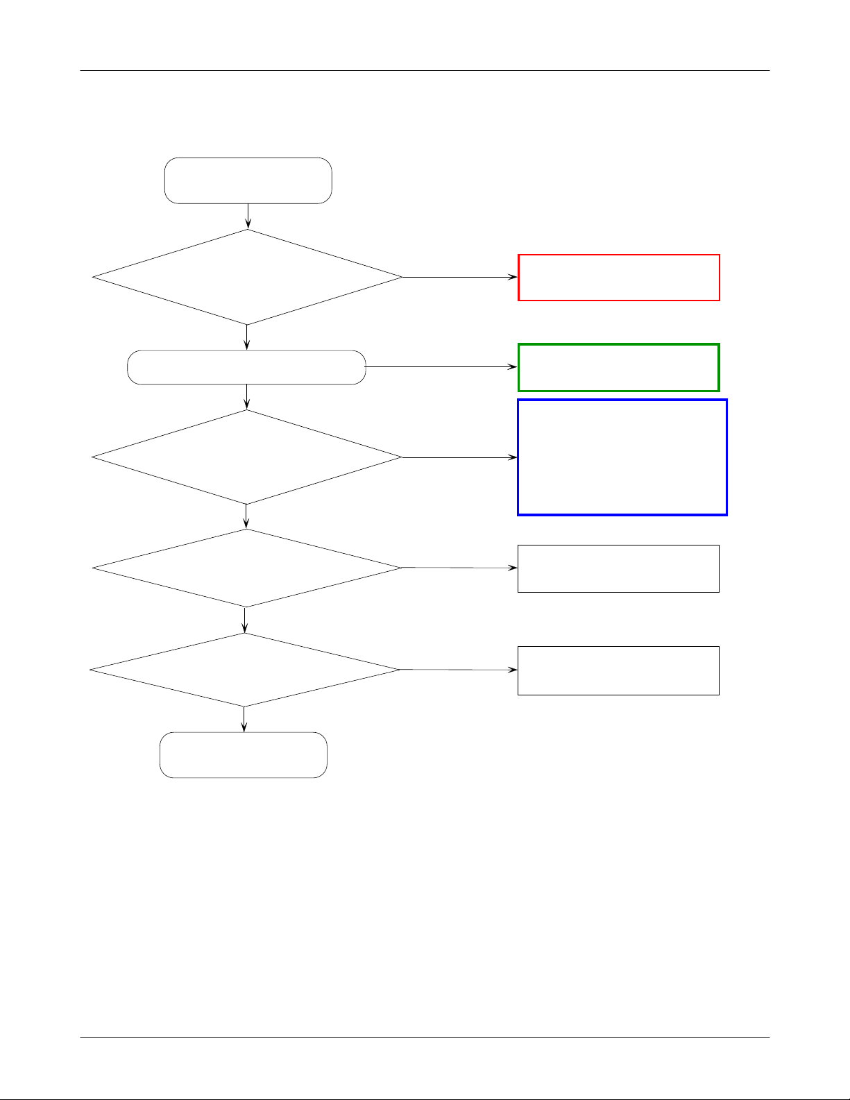
3-1-3. SIM Part
Flow Chart of Troubleshooting and Circuit Diagrams
"Please insert SIM card "
Check the SIM500's
Connection to SIM card
YES
Check the voltage at SIM500 pin
#1≒2.8V
YES
There is any signal pin#2,#3,#4
of SIM500
YES
Check the SIM Card
END
NO
NO
NO
Resolder or change SIM500
Check the U500
Check the U500 & UCP100
3-5
SAMSUNG Proprietary-Contents may change without notice
This Document can not be used without Samsung's authorization
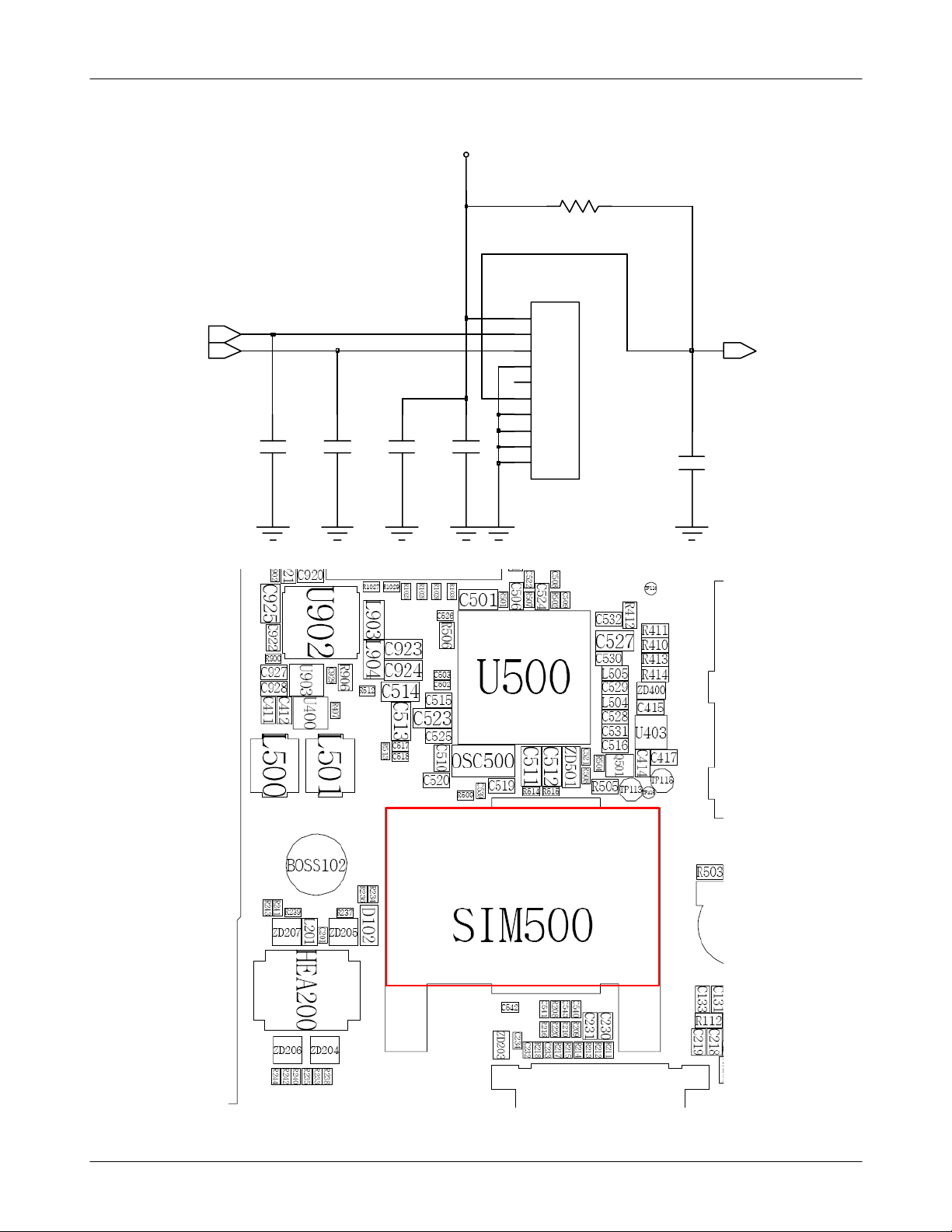
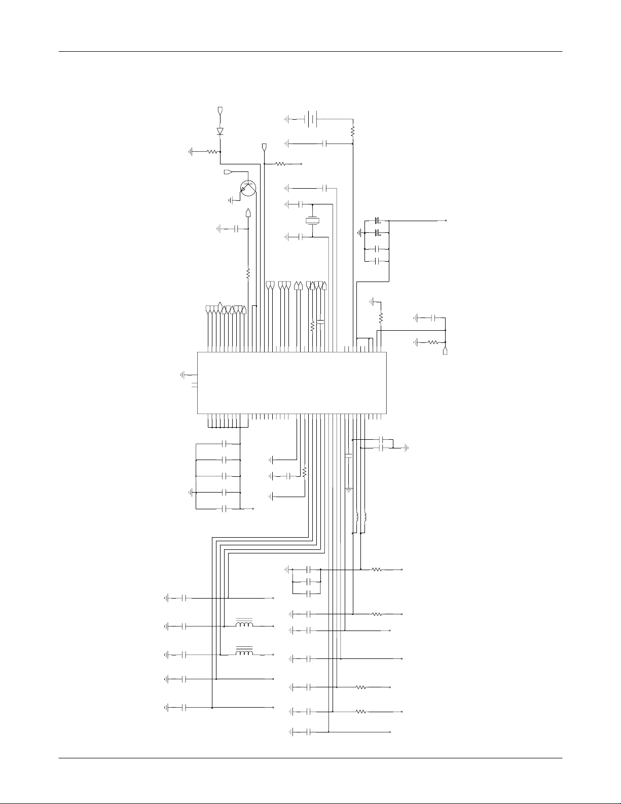
Flow Chart of Troubleshooting and Circuit Diagrams
USIM_RESET
USIM_CLK
C540
USIM_2.85V
C543C542C541
SIM500
1
2
3
4
5
6
7
8
9
10
VCC
VCC
CLK
GND
VPP
I/O
NC
NC
NC
NC
R509
USIM_DATA
C539
3-6
SAMSUNG Proprietary-Contents may change without notice
This Document can not be used without Samsung's authorization
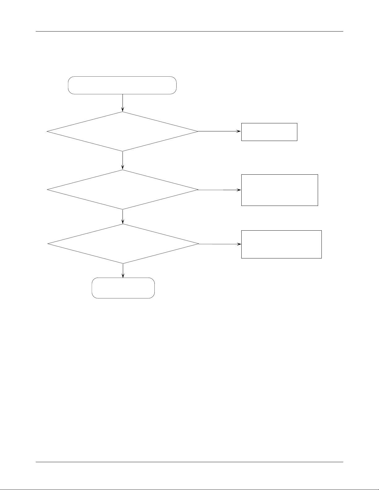
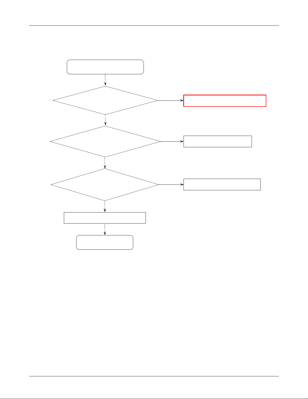
3-1-4. Charging Part
Abnormal charging operation
Flow Chart of Troubleshooting and Circuit Diagrams
Check the pin #13,14
of IFC200≥3.3V
YES
Check the pin #3
of BTC200≥3.3V
YES
See the indicator of charger is red ?
YES
END
NO
NO
NO
Check the TC
Check the path of
IFC200 and BTC200
Again, check the
IFC200
3-7
SAMSUNG Proprietary-Contents may change without notice
This Document can not be used without Samsung's authorization

Flow Chart of Troubleshooting and Circuit Diagrams
MICBIAS_2.85V
MIC2P
MIC2N
EAR_R
EAR_L
EAR_SW
JACK_IN
ADC_BOOTSW
ACC_OUT
RXD_1
JIG_ON_IF
USB_VCC
VEXT
C200
C203
R200
TA200
R202
R203
C206
C207
L202
C212
L204
C216
C217
C218
C219
VR200
VR201
RXD_2
R206
R207
MSMP_2.6V
R208 R209
BOOT_SW
D+
D-
R210
6
5
4
VR205
C227C226
R217
R218
C230
C231
R220
2
3
1
1
0
0
0
2
2
D
D
Z
Z
VR204
R211
R212
R213
R214
R215
9
0
2
D
Z
ACC_OUT_2
R216
3
C234C233C232
0
2
D
Z
TA204
VBAT
TDZ5.6
IFC200
1
1
2
2
3
3
4
4
5
5
6
6
7
7
8
8
9
9
10
10
11
11
12
12
13
13
14
14
15
15
16
16
17
17
18
18
19
19
20
20
21
NC
22
NC
23
NC
24
NC
25
NC5
26
NC6
BAT_VF
TCXO_2.85V
R223
C250
ZD202
D-2
D+2
JIG_ON_IF2
VBAT
1
2
3
4
BTC200
1
2
3
4
R227
R225
VR202
L200
TA206
3-8
SAMSUNG Proprietary-Contents may change without notice
This Document can not be used without Samsung's authorization
Flow Chart of Troubleshooting and Circuit Diagrams
3-9
SAMSUNG Proprietary-Contents may change without notice
This Document can not be used without Samsung's authorization

Flow Chart of Troubleshooting and Circuit Diagrams
3-1-5. Microphone Part
Micro-phone does not work
Is the assembled status of
Microphone O.K?
YES
Check the DC bias voltage on Mic path.
YES
The voltage of C214 is 2.3V?
YES
The microphone is OK
YES
NO
NO
NO
Reassemble the microphone
Check the path around MIC
Bias circuit
Check UCP100
END
3-10
SAMSUNG Proprietary-Contents may change without notice
This Document can not be used without Samsung's authorization
MICBIAS_2.85V
Flow Chart of Troubleshooting and Circuit Diagrams
MIC1P
MIC1N
C213
C222
TA201
C223
R205
C205
C209
R201
R204
C215
C221
C210
C211
L203
MIC200
C214
L205
C220
3-11
SAMSUNG Proprietary-Contents may change without notice
This Document can not be used without Samsung's authorization
Flow Chart of Troubleshooting and Circuit Diagrams
3-1-6. Speaker Part
There is no sound from speaker
The terminal of Speaker is OK
YES
There is signal
@U302pin#2
YES
There is signal
@ U304 R331
YES
The type of sound from
the Speaker is Media File?
YES
Are there any signal
atthepin#12,24ofU304?
NO
NO
NO
NO
NO
Replace the Speaker
Check the U302
Check the U304
The type of sound from
the Speaker is Melody.
Check the U300
Check the UCP100
YES
END
3-12
SAMSUNG Proprietary-Contents may change without notice
This Document can not be used without Samsung's authorization
VBAT
1
3
3
C
Flow Chart of Troubleshooting and Circuit Diagrams
ICE_AMP_OUT_P_L
RCVP
SPKL_SEL
ICE_AMP_OUT_N_L
SPKL-
RCVN
EAR_AMP_L
ICE_AMP_OUT_N_L
ICE_AMP_OUT_P_L
R327
C323
C325
MSM_EAR_L
R326
C332
SPKL+
ICEAMP_EN
L300
L302
C316
R315
C322
R331
R316
R310
C312
R314
C327
C313
1
1S2
2
1-2IN
3
2S1
4
D2
TA301
VBAT
8
1
2
C
N
R312
R320
RCVP
4
C
C
V
1
S
3
1
3-4IN
7
2
S
4
D4
4S1
3S2
3
D
3
1
2
1
1
1
0
R324
1
9
SPKR+
ICE_AMP_OUT_P_R
SPKR_SEL
RCVN
8
7
1
1
C
N
1
1
1
1
S
D
1
5
6
U302
D
2
N
S
2
G
6
5
SPKR-
ICE_AMP_OUT_N_R
MSM_EAR_R
R325
R308
24
22
23
18
16
15
19
21
C329
C314
U304
VREFR
VOMR
13
EN_R
12
VIPR
10
VIMR
11
6
C321
VOPR
4
2
VSS
5
VSS
8
VSS
14
VSS
17
VSS
20
VSS
25
GND
26
NC
27
NC
EN_L
VIPL
VIML
VREFL
VOPL
VOML
VDD
VDD
VDD
VDD
VDD
VDD
C315
R317
R311
R313
C318
C320
R318
L301
L303
R328
C340
YAMA_OUT_RYAMA_OUT_L
EAR_AMP_R
C324
C326
3-13
SAMSUNG Proprietary-Contents may change without notice
This Document can not be used without Samsung's authorization
 Loading...