

Samsung SGH-P100 Service Manual
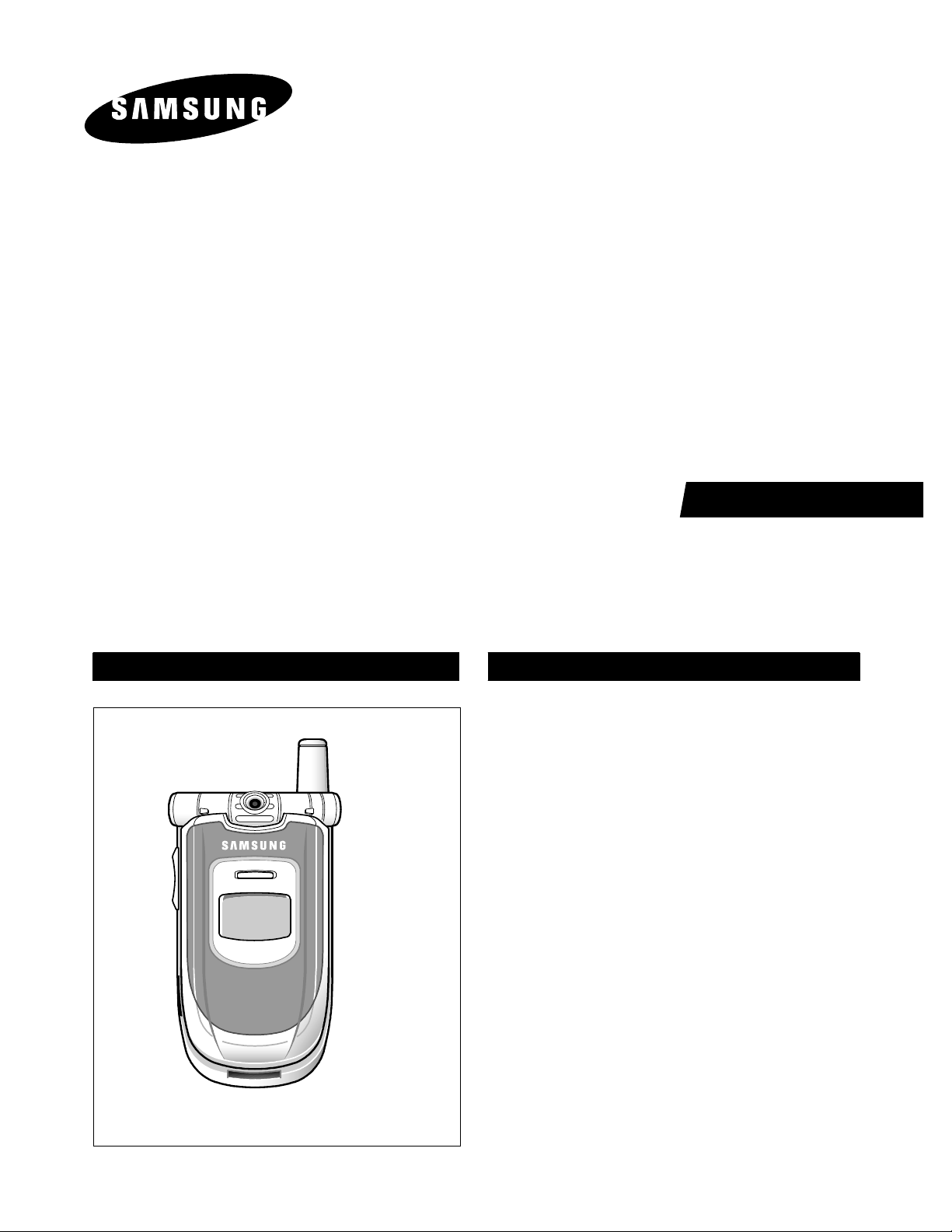
GSM TELEPHONE
SGH-P100
SERVICE
Manual
GSM TELEPHONE CONTENTS
1. Specification
2. Circuit Description
3. Exploded Views and Parts List
4. Electrical Parts List
5. Block Diagrams
6. PCB Diagrams
7. Flow Chart of Troubleshooting
ELECTRONICS
This Service Manual is a property of Samsung
Electronics Co.,Ltd.
Any unauthorized use of Manual can be punished
under applicable International and/or domestic law.
ⓒ
Samsung Electronics Co.,Ltd. August. 2003
Printed in Korea.
Code No.: GH68-03791A
BASIC.
1. SGH-P100 Specification
1-1
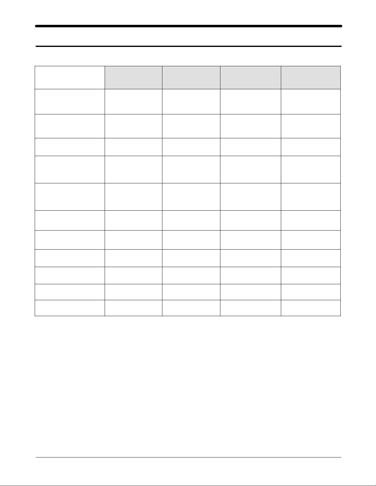
1. GSM General Specification
GSM900
Phase 1
Freq. Band[MHz]
Uplink/Downlink
ARFCN range 1~124
Tx/Rx spacing 45MHz 45MHz 95MHz 80MHz
Mod. Bit rate/
Bit Period
Time Slot
Period/Frame Period
Modulation 0.3GMSK 0.3GMSK 0.3GMSK 0.3GMSK
MS Power 33dBm~13dBm 33dBm~5dBm 30dBm~0dBm 30dBm~0dBm
890~915
935~960
270.833kbps
3.692us
576.9us
4.615ms
EGSM 900
Phase 2
880~915
925~960
0~124 &
975~1023
270.833kbps
3.692us
576.9us
4.615ms
DCS1800
Phase 1
1710~1785
1805~1880
512~885 512~810
270.833kbps
3.692us
576.9us
4.615ms
PCS1900
1850~1910
1930~1990
270.833kbps
3.692us
576.9us
4.615ms
Power Class 5pcl ~ 15pcl 5pcl ~ 19pcl 0pcl ~ 15pcl 0pcl ~ 15pcl
Sensitivity -102dBm -102dBm -100dBm -100dBm
TDMA Mux 8 8 8 8
Cell Radius 35Km 35Km 2Km -
This Document can not be used without Samsung's authorization
SAMSUNG Proprietary-Contents may change without notice
1-2
SGH-P100 Specification
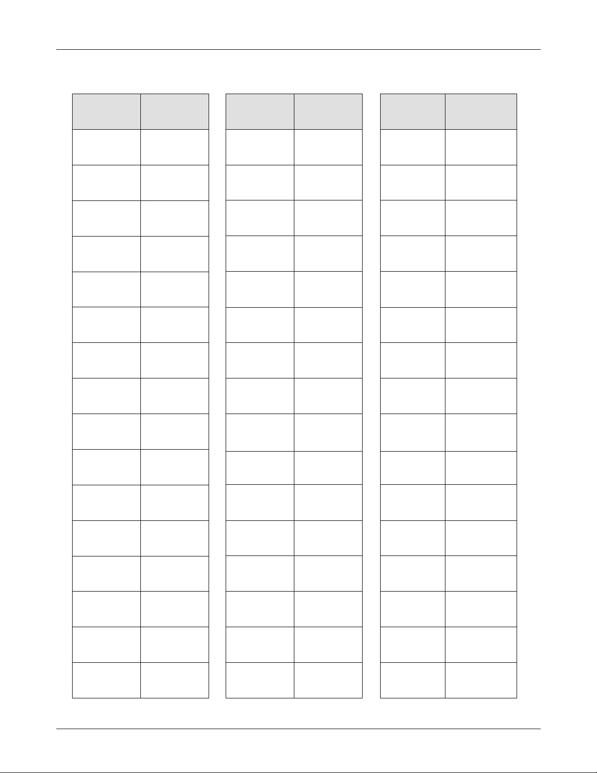
2. GSM TX power class
TX Power
control level
5 33±2 dBm
6 31±2 dBm
7 29±2 dBm
8 27±2 dBm
9 25±2 dBm
10 23±2 dBm
11 21±2 dBm
GSM900
TX Power
control level
0 30±2 dBm
1 28±3 dBm
2 26±3 dBm
3 24±3 dBm
4 22±3 dBm
5 20±3 dBm
6 18±3 dBm
DCS1800
TX Power
control level
0 30±2 dBm
1 28±3 dBm
2 26±3 dBm
3 24±3 dBm
4 22±3 dBm
5 20±3 dBm
6 18±3 dBm
PCS1900
12 19±2 dBm
13 17±2 dBm
14 15±2 dBm
15 13±2 dBm
16 11±3 dBm
17 9±3dBm
18 7±3 dBm
19 5±3 dBm
7 16±3 dBm
8 14±3 dBm
9 12±4 dBm
10 10±4 dBm
11 8±4dBm
12 6±4 dBm
13 4±4 dBm
14 2±5 dBm
7 16±3 dBm
8 14±3 dBm
9 12±4 dBm
10 10±4 dBm
11 8±4dBm
12 6±4 dBm
13 4±4 dBm
14 2±5 dBm
15 0±5 dBm
15 0±5 dBm
This Document can not be used without Samsung's authorization
SAMSUNG Proprietary-Contents may change without notice
2. SGH-P100 Circuit Description
2-1
1. SGH-P100 RF Circuit Description
1) RX PART
1. ASM(U1001)→Switching Tx, Rx path for GSM900, DCS1800 and PCS1900 by logic controlling.
2. ASM Control Logic (U701, U702, U703)→Truth Table
VC1 VC2 VC3
GSM Tx Mode H L L
DCS / PCS Tx Mode L H L
PCS Rx Mode L L H
GSM / DCS Rx Mode L L L
3. FILTER
To convert Electromagnetic Field Wave to Acoustic Wave and then pass the specific frequency band.
- GSM FILTER (C1003,C1004,L1001)→For filtering the frequency band between 925 ~ 960 MHz
- DCS FILTER (C1005,C1006,L1002)→For filtering the frequency band 1805 and 1880 MHz.
- PCS SAW FILTER (F1003)→For filtering the frequency band between 1930 and 1990 MHz
4. TC-VCXO (OSC901)
To generate the 13MHz reference clock to drive the logic and RF.
After additional process, the reference clock applies to the U900 Rx IQ demodulator and Tx IQ modulator.
The oscillator for RX IQ demodulator and Tx modulator are controlled by serial data to select channel and use fast lock
mode for GPRS high class operation.
5. SI 4205 (U900)
This chip integrates three differential-input LNAs.
The GSM input supports the E-GSM, DCS input supports the DCS1800, PCS input supports the PCS1900. The LNA
inputs are matched to the 150 ohm differential output SAW filters through external LC matching network.
Image-reject mixer downconverts the RF signal to a 100 KHz intermediate frequency(IF) with the RFLO from frequency
synthesizer. The RFLO frequency is between 1737.8 ~ 1989.9 MHz.
The Mixer output is amplified with an analog programmable gain amplifier(PGA), which is controlled by AGAIN.
The quadrature IF signal is digitized with high resolution A/D converts (ADC).
Also, this chip down-converts the ADC output to baseband with a digital 100 KHz quadrature LO signal. Digital
decimation and IIR filters perform channel selection to remove blocking and reference interface signals.
After channel selection, the digital output is scaled with a digital PGA, which is controlled with the DGAIN. DACs drive
a differential analog signal onto the RXIP, RXIN, RXQP, RXQN pins to interface to standard analog-input baseband IC.
This Document can not be used without Samsung's authorization
SAMSUNG Proprietary-Contents may change without notice
2-2
SGH-P100 Circuit Description
2) TX PART
Baseband IQ signal fed into offset PLL, this function is included inside of U900 chip.
SI4205 chip generates modulator signal which power level is about 1.5dBm and fed into Power Amplifier(U1000).
The PA output power and power ramping are well controlled by Auto Power Control circuit. We use offset PLL below
GSM -35dBc
DCS -35dBc
PCS -35dBc
GSM -66dBc
DCS -65dBc
PCS -66dBc
GSM -75dBc
DCS -68dBc
PCS -75dBc
Modulation Spectrum
200kHz offset
30 kHz bandwidth
400kHz offset
30 kHz bandwidth
600kHz ~ 1.8MHz offset
30 kHz bandwidth
2. Baseband Circuit description of SGH-P100
1. PSC2006
1.1. Power Management
Seven low-dropout regulators designed specifically for GSM applications power the terminal and help ensure optimal
system performance and long battery life. A programmable boost converter provides support for 1.8V, 3.0V, and 5.0V
SIMs, while a self-resetting, electronically fused switch supplies power to external accessories. Ancillary support functions,
such as an LED driver and two call-alert drivers, aid in reducing both board area and system complexity.
A three-wire serial interface unit(SIU) provides access to control and configuration registers. This interface gives a
microprocessor full control of the PSC2006 and enables system designers to maximize both standby and talk times.
Supervisory functions. including a reset generator, an input voltage monitor, and a thermal monitor, support reliable system
design. These functions work together to ensure proper system behavior during start-up or in the event of a fault
condition(low microprocessor voltage, insufficient battery energy, or excessive die temperature).
1.2. Battery Charge Management
A battery charge management block provides fast, efficient charging of a single-cell Li-ion battery . Used in conjunction
with a current-limited voltage source and an external PMOS pass transistor, this block safely conditions near-dead cells
and provides the option of having fast-charge and top-off controlled internally or by the system's microprocessor.
1.3. Backlight LED Driver
The backlight LED driver is a low-side, programmable current source designed to control the brightness of the keyboard
and LCD illumination. The driver is enabled by EN_LED, and its current setting is determined by LED[0:2]. Provided
EN_LED is‘1’, the driver can be programmed to sink from 12.5mA to 100mA in 12.5mA steps. LED_DRV is
capable of sinking 100mA at a worst-case maximum output voltage of 0.6V. For efficient use, the LEDs is connected
between the battery and the LED_DRV output.
This Document can not be used without Samsung's authorization
SAMSUNG Proprietary-Contents may change without notice

SGH-P100 Circuit Description
2-3
1.4. Vibrator Motor Dirver
The vibrator motor driver is a low-side, programmable voltage source designed to drive a small dc motor that silently
alerts the user of an incoming call. The driver is enabled by EN_VIB, and its voltage setting is determined by VIB[0:2].
Provided EN_VIB is a logic 1, the driver can be programmed to maintain a motor voltage of 1.1V to 2.5V in 20mV
steps and while sinking up to 100mA. For efficient use, the vibrator motor should be connected between the main battery
and the VIB_DRV output.
2. Connector
2-1. LCD Connector
LCD is consisted of main LCD(color 65K STN LCD) and small LCD(4-gray LCD). Chip select signals of EMI part in
the trident, CLCD_EN_FO and GLCD_EN_FO, can enable Each LCD. LED_EN_FO signal enables white LED of main
LCD and EL_EN_FO signal enables EL of small LCD. These two signals are from IO part of the DSP in the trident.
RST signal from 2006 initiates the initial process of the LCD.
16-bit data lines(D(0)_FO~D(15)_FO) transfers data and commands to LCD through emi_filter. Data and commands use
A(2)_FO signal. If this signal is high, Inputs to LCD are commands. If it is low, Inputs to LCD are data. The signal
which informs the input or output state to LCD, is required. But this system is not necessary this signal. So
CP_WEN_FO signal is used to write data or commands to LCD. Power signals for LCD are V_bat and V_ccd.
SPK1P and SPK1N from CSP1093 are used for audio speaker. And VIB_EN_FO from enables the motor.
2-2. JTAG Connector
Trident has two JTAG ports which are for ARM core and DSP core(DSP16000). So this system has two port connector
for these ports. Pins’initials for ARM core are‘CP_’and pins’initials for DSP core are‘DSP_’. CP_TDI and
DSP_TDI signal are used for input of data. CP_TDO and DSP_TDO signals are used for the output of the data. CP_TCK
and DSP_TCK signals are used for clock because JTAG communication is a synchronous. CP_TMS and DSP_TMS
signals are test mode signals. The difference between these is the RESET_INT signal which is for ARM core RESET.
2-3. IRDA
This system uses IRDA module, HSDL_3201, HP’s. This has signals, IRDA_EN(enable signal), IRDA_RX(input data)
and IRDA_TX(output data). These signals are connected to PPI of trident. It uses two power signals. V_ccd is used for
circuit and V_bat is used for LED.
2-4. Keypad connector
This is consisted of key interface pins among PPI in the trident, KEY_ROW[0~4] and KEY_COL[0~4]. These signals
compose the matrix. Result of matrix informs the key status to key interface in the trident. Some pins are connected to
varistor for ESD protection. And power on/off key is seperated from the matrix. So power on/off signal is connected with
PSC2006 to enable PSC2006. SVC_GREEN, SVC_RED and SVC_BLUE are from OCTL of CSP1093. These signals
decide the color of LED, service indicator. Eighteen key LED use the V_bat supply voltage. These are connected to
BACKLIGHT signal in the PSC2006. This signal enables LEDs with current control. FLIP_SNS informs the status of
folder (open or closed) to the trident. This uses the hall effect IC, A3210ELH. A magnet under main LCD enables
A3210ELH which is on the key FPCB.
This Document can not be used without Samsung's authorization
SAMSUNG Proprietary-Contents may change without notice

2-4
SGH-P100 Circuit Description
3. IF connetor
It is 24-pin connector, and uses 18-pin at present. They are designed to use SDS, DEBUG, DLC-DETECT, JIG_ON,
VEXT, VTEST, VF, CF, VBAT and GND. They connected to power supply IC, microprocessor and signal processor IC.
4. Audio
AOUTAP from CSP1093 is connected to the main speaker. AOUTAN is connected to the speaker via audio-amp.
AOUTBN and AOUTBP are connected to the ear-mic speaker via ear-jack. MICIN and MICOUT are connected to the
main MIC. And AUXIN and AUXOUT are connected to the Ear-mic.
YMU762MA3 is a LSI for portable telephone that is capable of playing high quality music by utilizing FM synthesizer
and ADPCM decorder that are included in this device.
As a synthesis, YMU762MA3 is equipped 16 voices with differenttones. Since the device is capable of simultaneously
generating up to synchronous with the play of the FM synthesizer, various sampled voices can be used as sound effects.
Since the play data of YMU762MA3 are interpreted at anytime through FIFO, the length of the data(playing period) is
not limited, so the device can flexiblysupport application such as incoming call melody music distribution service. The
hardware sequencer built in this device allows playing of the complex music without giving excessive load to the CPU of
the portable telephones. Moreover, the registers of the FM synthesizer can be operated directly for real time sound
generation, allowing, for example, utilization of various sound effects when using the game software installed in the
portable telephone.
YMU759 includes a speaker amplifier with high ripple removal rate whose maximum output is 550mW (SPVDD=3.6V).
The device is also equipped with conventional function including a vibartor and a circuit for controlling LEDs
synchornous with music.
For the headphone, it is provided with a stereophonic output terminal.
For the purpose of enabling YMU762MA3 to demonstarte its full capablities, Yamaha purpose to use "SMAF:Synthetic
music Mobile Application Format" as a data distribution format that is compatible wiht multimedia. Since the SMAF takes
a structure that sets importance on the synchronization between sound and images, various contents can be written into it
including incoming call melody with words that can be used for traning karaoke, and commercial channel that combines
texts, images and sounds, and others. The hardware sequencer of YMU762MA3 directly interprets and plays blocks
relevant to systhesis (playing music and reproducing ADPCM with FM synthesizer) that are included in data distributed in
SMAF.
5. Memory
This system uses SHARP’s memory, LRS1828. It is consisted of 128M bits flash memory and 32M bits SCRAM.
It has 16 bit data line, D[0~15] which is connected to trident, LCD or CSP1093. It has 22 bit address lines, A[1~22].
They are connected too. CP_CSROMEN and CO_CSROM2EN signals, chip select signals in the trident enable two
memories. They use 3 volt supply voltage, V_ccd and 1.8 volt supply voltage, Vcc_1.8a in the PSC2006. During wrting
process, CP_WEN is low and it enables writing process to flash memory and SRAM. During reading process, CP_OEN
is low and it output information which is located at the address from the trident in the flash memory or SRAM to data
lines. Each chip select signals in the trident select memory among 2 flash memory and 2 SRAM. Reading or writing
procedure is processed after CP_WEN or CP_OEN is enabled. Memories use FLASH_RESET, which is buffered signal of
RESET from PSC2006, for ESD protection. A[0] signal enables lower byte of SRAM and UPPER_BYTE signal enables
higher byte of SRAM.
This Document can not be used without Samsung's authorization
SAMSUNG Proprietary-Contents may change without notice

SGH-P100 Circuit Description
2-5
6. Trident
Trident is consisted of ARM core and DSP core. It has 20K*16bits RAM 144K*16bits ROM in the DSP. It has
4K*32bits ROM and 2K*32bits RAM in the ARM core. DSP is consisted of timer, one bit input/output unit(BIO), JTAG,
EMI and HDS(Hardware Development System). ARM core is consisted of EMI, PIC(Programmable Interrupt Controller),
reset/power/clock unit, DMA controller, TIC(Test Interface Controller), peripheral bridge, PPI, SSI(Synchronous Serial
Interface), ACC(Asynchronous communications controllers), timer, ADC, RTC(Real-Time Clock) and keyboard interface.
DSP_AB[0~8], address lines of DSP core and DSP_DB[0~15], data lines of DSP core are connected to CSP1093.
A[0~20], address lines of ARM core and D[0~15], data lines of ARM core are connected to memory, LCD and YMU759.
ICP(Interprocessor Communication Port) controls the communication between ARM core and DSP core.
CSROMEN, CSRAMEN and CS1N to CS4N in the ARM core are connected to each memory. WEN and OEN control
the process of memory. External IRQ(Interrupt ReQuest) signals from each units, such as, YMU, Ear-jack, Ear-mic and
CSP1093, need the compatible process.
Some PPI pins has many special functions. CP_KB[0~9] receive the status from key FPCB and are used for the
communicatios using IRDA(IRDA_RX/TX/EN) and data link cable(DEBUG_DTR/RTS/TXD/RXD/CTS/DSR). And
UP_CS/SCLK/SDI, control signals for PSC2006 are outputted through PPI pins. It has signal port for charging(CHG_DET,
CHG_STAT0), SIM_RESET and FLIP_SNS with which we knows open.closed status of folder. It has JTAG control
pins(TDI/TDO/TCK) for ARM core and DSP core. It recieves 13MHz clock in CKI pin from external TCXO and receives
32.768KHz clock from X1RTC. ADC(Analog to Digital Convertor) part receives the status of temperature, battery type
and battery voltage. And control signals(DSP_INT, DSP_IO and DSP_RWN) for DSP core are used. It enables main LCD
and small LCD with DSP IP pins.
7. CSP1093
CSP1093 integrates the timing and control functions for GSM 2+ mobile application with the ADC and DAC functions.
The CSP1093 interfaces to the trident, via a 16-bit parallel interface. It serves as the interface that connects a DSP to the
RF circuitry in a GSM 2+ mobile telephone. DSP can load 148 bits of burst data into CSP1093’s internal register, and
program CSP1093’s event timing and control register with the exact time to send the burst. When the timing portion of
the event timing and control register matches the internal quarter-bit counter and internal frame counter, the 148 bits in
the internal register are GMSK modulated according to GSM 2+ standards. The resulting phase information is translated
into I and Q differential output voltages that can be connected directly to an RF modulator at the TXOP and TXON pins.
The DSP is notified when the transmission is completed. For receiving baseband data, a DSP can program CSP1093’s
event timing and control register with the exact time to start receiving I and Q samples through TXIP and TXIN pins.
When that time is reached, the control portion of the event timing and control register will start the baseband receive
section converting I and Q sample pairs. The samples are stored in a double-buffered register until the register contains
32 sample pairs. CSP1093 then notifies the DSP which has ample time to read the information out before the next 32
sample pairs are stored. The voice band ADC converter issues an interrupt to the DSP whenever it finishes converting a
16-bit PCM word. The DSP then reads the new input sample and simultaneously loads the voice band output DAC
converter with a new PCM output word. The voice band output can be connected directly to a speaker via AOUTAN and
AOUTAP pins and be connected to a Ear-mic speaker via AOUTBN and AOUTBP pins.
8. X-TAL(13MHz)
This system uses the 13MHz TCXO, TCO-9141B, Toyocom. AFC control signal form CSP1093 controls frequency from
13MHz x-tal. It generates the clock frequency. This clock is inverted through NOT gate, TC7S04FU and is connected to
CSP1093. 13MHz clock for YMU759 uses a not-inverted clock. Clock for RF parts uses same ty pe.
This Document can not be used without Samsung's authorization
SAMSUNG Proprietary-Contents may change without notice

2-6
SGH-P100 Circuit Description
9.Camera DSP(LC99704B)
- This chipset is MCP product that combines the CCD Driver with on-chip booster circuit
and analogue/digital mixed-signal processing IC.
The booster circuit generate the supply voltages required for CCD drive.
Cameras can use either a +2.8V or +3.0V or +3.3V only power supply system.
The analogue / digital mixed-signal processing IC that integrates the signal-processing
functions required in a CCD digital camera and a rich set of addtional functions on a single
chip. Although the CDS(correlated dual sampling) and AGC circuit required for analog
processing and the clamp circuit required for A/D conversion are normally povided on
circuits, as well as an A/D converter, on a single chip.
Additionally, it also includes the pulse generator circuits required for CCD drive, the
logic circuits for the electronics iris, and the digital signal-processing circuits required to
create the digital YUV signal output. This device can take advantage of the features of
these digital signal-processing functions to provide auto white balance, automatic dropout
detection and correction, mirror image output, and a single line of memory to provide
flexibility in the external interface.
This device assumes an internal master clock frequency in the range 16 ~27 MHz.
Normally , either an external clock with that frequency is provided, or else a master clock
oscillator circuit is constructed using the built-in oscillator inverter circuit.
And this is also possible to control the CCD drive internal and enternal.
10. Camera ASIC(SSH 275)
This ASIC interfaces between CCD and LCD, and this chip compresses and expands
input pictures from CCD with JPEG format.
- CCD I/F : YUV422(16 bit) format, CIF fixed size.
System clock providing CCD module (13.5 MHz) and Dot clock providing
CCD module (13.5 MHz).
- CPU I/F : Accessible to JPEG controller, a control register including, JPEG code buffer,
and a thumbnail picture buffer.
Direct access to LCD controller by switching buses.
- LCD I/F : Support LCD controller.
Accessible by switching 2 masters of the Host CPU or ASIC picture
processing .
Output format from ASIC is RGB565.
- I2C I/F : I2C master for CCD module control equipped.
CCD module is accessible from CPU wiithout paying attention to I2C, as in the
case of a normal register write/read.
- JPEG codec : YUV422 picture data is compressed to JPEG code, and JPEG code data is
expanded to YUV422 picture data.
- Clock system : As for ASIC, 27 MHz clock input from outside is the main clock.
2-divided 13.5 MHz is used as CCD module main clock output, dot clock
output to CCD module, and ASIC inner clock
This Document can not be used without Samsung's authorization
SAMSUNG Proprietary-Contents may change without notice
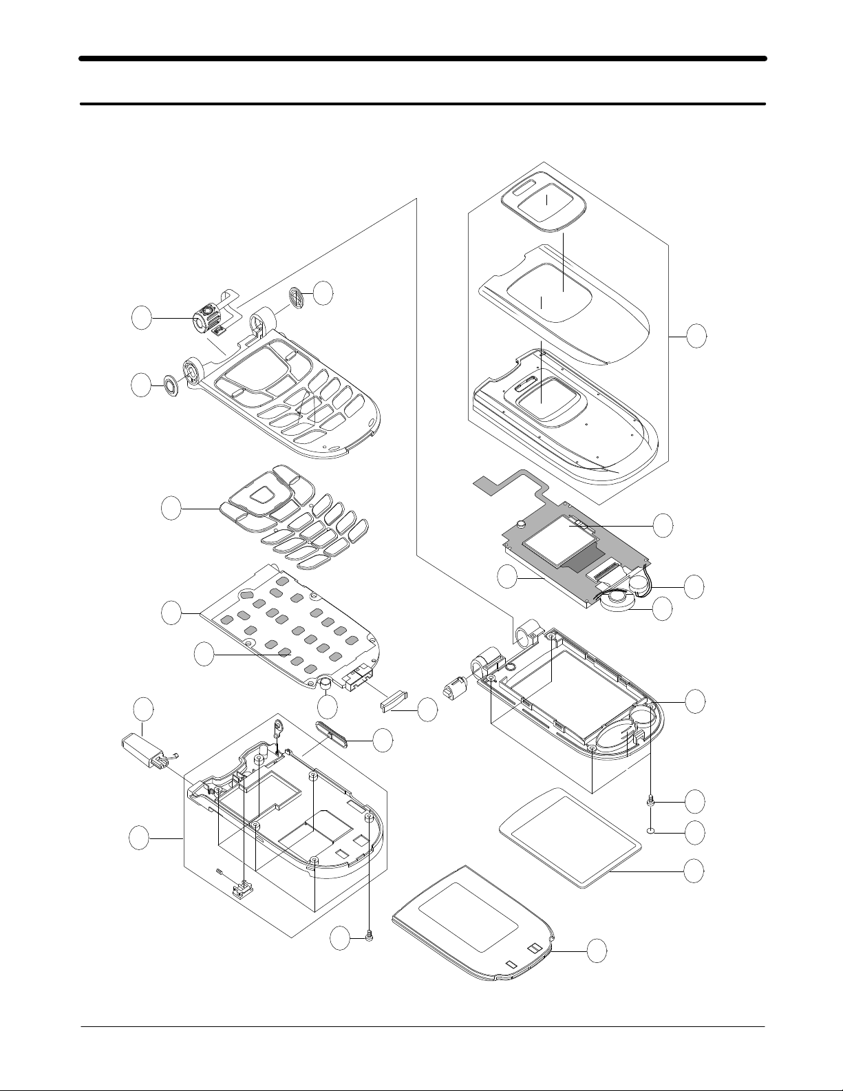
3. SGH-P100 Exploded View and its Parts list
3-1
1. Cellular phone Exploded View
12
10
11
1
20
19
13
14
15
16
18
17
2
5
3
4
6
7
8
9
21
22
This Document can not be used without Samsung's authorization
SAMSUNG Proprietary-Contents may change without notice
3-2
SGH- P100 Exploded view and its Part list
2. Cellular phone Parts list
Location
NO.
1
2 LCD FPCB GH07-00358A
3 MOTOR 3101-001336
4 SPEAKER 3001-001427
5 MAIN LCD GH07-00253A
6 FOLDER LOWER GH75-03191A
7 SCREW 6001-001478
8 SCREW CAP GH74-02775A
9 MAIN WINDOW GH75-03362A
10 CAMERA GH59-00806A
FOLDER UPPER
Description SEC CODE Remark
GH75-03160A
11 SIDE DECO GH72-08113A
12 SIDE DECO GH72-08113A
13 KEYPAD GH75-03148A
14 MAIN PBA GH92-01514A
15 METAL DOME SHEET GH59-00821A
16 MIC GH30-00029A
17 IF COVER GH73-02150A
18 VOLKEY GH75-03230A
19 ANTENNA GH42-00304A
20 REAR COVER GH75-03195A
21 SCREW 6001-001155
22 BATTERY GH43-00906A
This Document can not be used without Samsung's authorization
SAMSUNG Proprietary-Contents may change without notice
 Loading...