

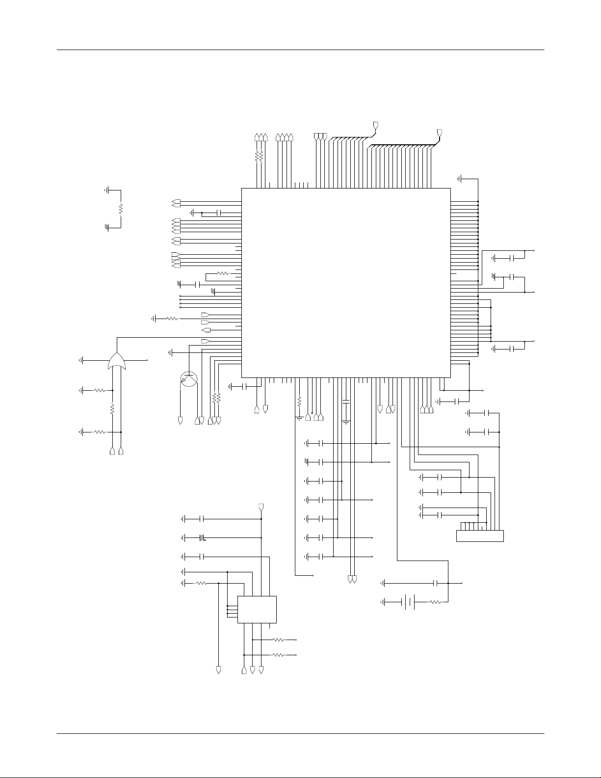
Samsung SGH-N707 Block Diagram
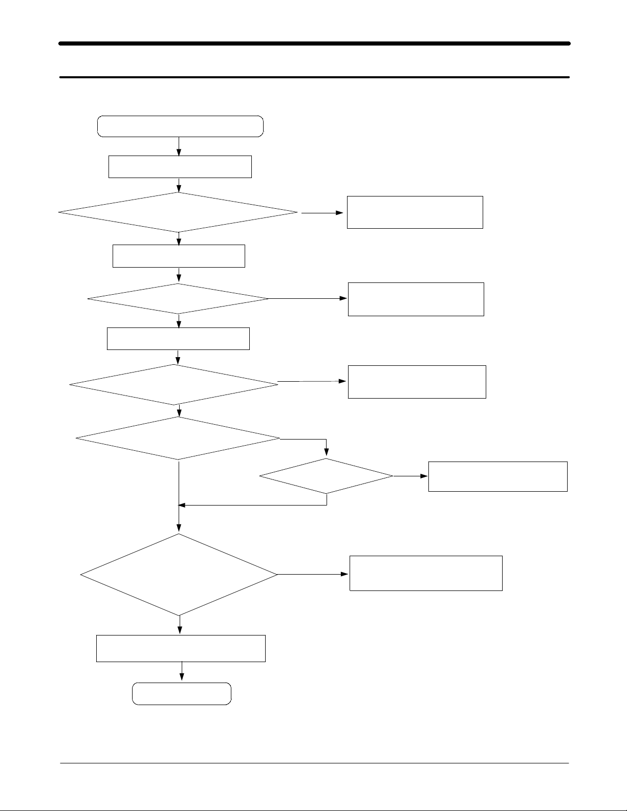
7. SGH-N707 Flow Chart of Troubleshooting
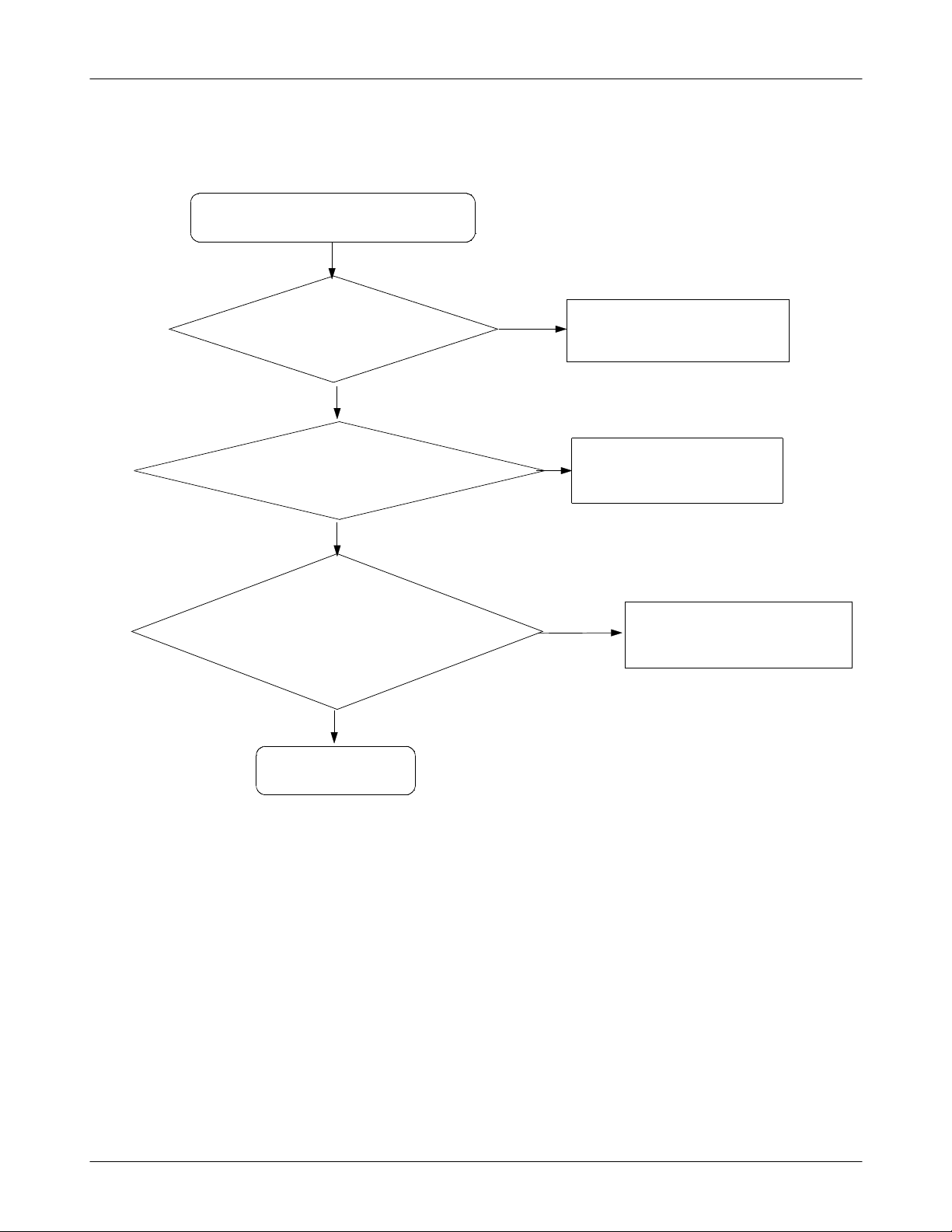
1. Power On
The set is not ' Power On '
Check the current consumption
Current consumption
>=100mA
Yes
Check the +VBATT Voltage
Voltage >= 3.3V
Yes
Check the pin of U101
pin#J12 of U101 >= 2.8V
Yes
pin#A13 of U101 = 2.8V
Yes
No
No
No
No
pin#G11 = 1.8V
Download again
Charge the Battery
Check U101 and C112
No
Check U101 and C115
Check the clock signal
at pin#R6
Freq = 13MHz
Yes
Check the initial operation
END
SAMSUNG Proprietary-Contents may change without notice
This Document can not be used without Samsung's authorization
Yes
No
7-1
Check the clock generation circuit
(related to OSC401)
Flow Chart of Troubleshooting
2. Initial
Initialization Failure
Yes
The pin#G11 of U101 = 1.8V
the pin#J12 of U101 ≒ 2.825V
Is the pin#K9 of U101
32.768kHz wave forms at
the C220 and C221
The Voltage is "High" at
and
?
Yes
"Low -> High"?
Yes
Yes
the C112
No
No
No
No
(If it has some problem, adjust it.)
Check the U101
Check the U101
(If it has some problem, adjust it.)
Check the U201
Check the U101
Yes
No
LCD display is O.K
Yes
No
Sound is O.K
Yes
END
7-2
SAMSUNG Proprietary-Contents may change without notice
This Document can not be used without Samsung's authorization
Check the LCD Part
Check the Audio Part
Flow Chart of Troubleshooting
VCCD
VCCA
VCCD
CHG_DET
100K
100K
AGND
TC7S32FU
3
R112
R111
GND
A
2
R110
TA_VEXT
DSP_AB(5)
DSP_AB(4)
M2
N2
AB4
AB5M1AB6
VLDO_4
VL4S_A
B12
A12
C122
470nF
GSM_TX_EN
DSP_AB(7)
DSP_AB(6)
VLDO_5
VL4S_B
B11
DCS_TX_EN
DSP_AB(0:8)
DSP_AB(8)
DSP_DB(4)
DSP_DB(3)
DSP_DB(2)
DSP_DB(1)
DSP_DB(0)
K2
K3
K7
K5
J5
DB3J6DB4
DB0K1DB1
DB2
AB7
AB8
CSP2200B1
U101
RING_DRV
VIB_DRV
VLDO_6
VLDO_7
VL5S_A
VL5S_B
B10
A14
C12
F15
D10
C9
F13
VIB_EN
BL_KEY_LED
VR
F
VCCD
VCC_1.8A
DSP_DB(6)
DSP_DB(5)
H5
G3
DB5
DB6
LED1_DRV
LED2_DRV
G13
G12
FL_LED
VCCB
VCCA
DSP_DB(8)
DSP_DB(7)
DSP_DB(9)
F1
DB7G4DB8F4DB9
VRTC
VSI
M
K12
H11
NEG
2
RB414_IV02N
BAT101
TX_BAND_SEL
SERDAT
SERLE
SERCLK
TX_EN
SI_EN
R113
R103
100
100
A3
C2
C1
B3
SERDAB1SERLE1A2SERLE2
SERCK
H10
RTCALARM
3
GND
_ACOK
6
CREF
E9
VREF
TA_VEXT
2IN4
BATT
7
VREF
A10
ADC_AUX1
ADC_AUX2
E10
D15
1
VL
_CHG
8
100K
NC
OCTL7
CH_RES
D14
MAX1508ETA
U107
R114
R115
R108
0
U102
4
Y
5
VCC
B
1
VBAT
TXPOWER
RXTXIP
RXTXIN
RXTXQP
RXTXQN
AOUTAP
AOUTAN
MICINP
MICINN
MICOUTP
MICOUTN
AFC
TP102
TP103
TP104
TP105
0
AGND
R102
CLK13M_MC
DTC144EM
Q102
2
CLK32K
DSP_INT
PWR_ON
1
3
C120
1UF
6.3V
C119 100NF
R104
AGND
R105
R106
0
0
D9
AFC
E7
TXP
B5
RAREF2
B6
RAREF1
D7
RXTXIP
D6
RXTXIN
C7
RXTXQP
C6
RXTXQN
P11
AOUTAP
N12
AOUTAN
R12
AOUTBP
P12
AOUTBN
N14
MICINP
M14
MICINN
N15
MICOUTP
P15
MICOUTN
M15
AUXINP
0
L14
AUXINN
K13
AUXOUTP
L13
AUXOUTN
R13
VXVCM
M13
VREGP
R14
VREGN
R4
DAICK
P4
DAIRN
L6
DAIDI
M6
DAIDO
N4
RTC_CLK
D1
XOENAQ
R6
MC
P5
NC7
P3
DINTR
C14
PWR_SW2
C15
PWR_SW1N
L7
PSW1_BUF
K9
RESET_O
N10
MODE
M9
PWR_KEEP
L10
INTRQ
L9
VIB_RNG_EN
RTC_ALMN
C118
220NF
10K
PWR_KEEP
RST
MELODY_VI
KEY_COL(2)
KEY_ROW(0)INTRQ
B
JIG_ON
C124
100NF
C123
10UF
10V
470nF
C121
R107
2.7K
, 1%
ISET
G
9
G
10
GG
11
12
_EN
5
XOENA
OCTL5G6OCTL6
CH_BDRV
CH_ISEN
F12
FLASH_RESET
DSP_RW
DSP_I
O
N
DSP_AB(3)
DSP_AB(2)
DSP_AB(1)
DSP_AB(0)
C5
R3
K6
P1
L2
E6
F5
E5
OCTL3A4OCTL4
VBAT
E13
E11
VEXT
OCTL2
E14
OCTL1
OCTL0
SDI_PSC
M7
RESETN_CSP
SCLK_PSC
SDO_PSC
L8
N7
RW
I|O
N
CSN_PSC
K8
L3
AB0
AB1L5AB2N1AB3
VLDO_2
VLDO_3
VLDO_1
VACC
G11
J1
A13
F14
2
R109
10K
TP106
UP_SCLK
UP_SDI
UP_CS
470NF
C113
AGND
16V
C116
2.2UF
C114
56PF
16V
C111
2.2UF
100NF
C117
16V
C112
2.2UF
1UF
6.3V
C115
VBAT
VCCD
VCCD
DSP_DB(11)
DSP_DB(10)
F2
DB10
DB11F3DB12E2DB13E3DB14
SIM_CLK
SIM_RST
K14
PO
S
1
DSP_DB(13)
DSP_DB(12)
SIM_IO
UP_I
O
J11K11
P10
SIMDATA
SIMRST
DSP_DB(15)
DSP_DB(14)
D3
D2
DB15
GND_HCUR
UP_CLK
UP_RST
N9
R10
SIMCLK
100PF
1.2K
DSP_DB(0:15)
GNDS17
GNDS16
GNDS15
GNDS14
GNDS13
GNDS12
GNDS11
GNDS10
GNDS9
GNDS8
GNDS7
GNDS6
GNDS5
GNDS4
GNDS3
GNDS2
GNDS1
AUX_ADC3
GND_OCTL
VDD_OCTL
GNDV
VDDV
GNDB
VDDB
GNDD
VDDD
VDD_IO2
VDD_IO1
VDD3
VDD2
VDD1
GND_PSC2
GND_PSC1
GNDQ
VDD67
VDD5
VDD12
J1
3
C108
33PF
C109
33PF
33PF
C107
C110
R101
2
NC6
1
NC5
K10
J10
J9
J8
J7
H9
H8
H7
H6
G10
G9
G8
G7
F10
F9
F8
F7
D13
B4
C4
P13
L11
F6
A6
M10
N11
P6
VSS4
R2
VSS3
K4
VSS2
G5
VSS1
J4
N5
N6
M3
J3
F11
K15
B15
E8
B13
C10
VDD34
C11
10V
C104
2.2UF
(rf-5000-6P-2.2L)
7NC8NC9
5000-6P-2.2L
NC10NC
VRT
C
C102
56PF
AGND
C101
56PF
C103
100NF
VBAT
2.2UF
C105
10V
C106
100NF
5
4
6
VCC1VCC2VPP
CLK3GND
I/O
CN101
CHG_ON
ICHRG
VBAT
7-3
SAMSUNG Proprietary-Contents may change without notice
This Document can not be used without Samsung's authorization
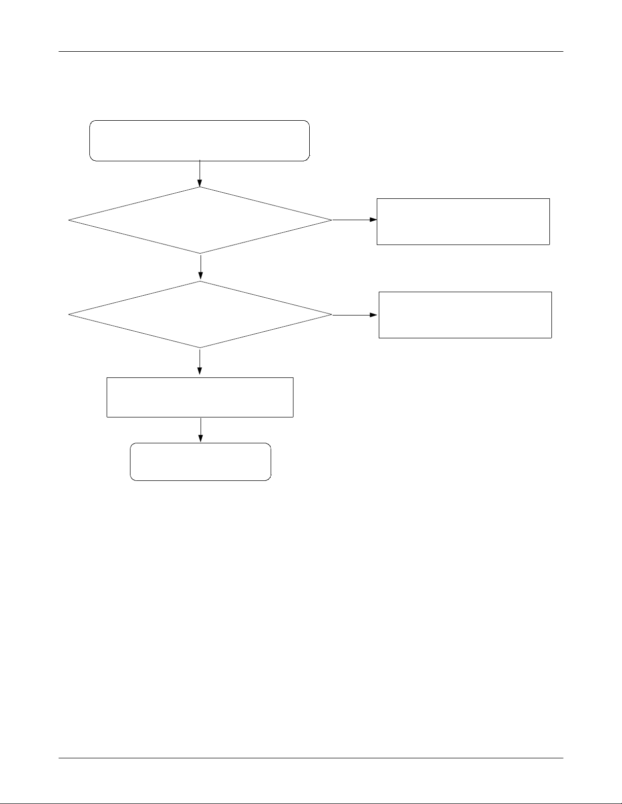
Flow Chart of Troubleshooting
3. SIM Part
"Insert SIM" is displayed on the LCD
Are there any Signals at
pin#N9, #R10, #P10 of U101?
Yes
No
Check the U102
Yes
Are there any Signals at
pin#K12, #K11, #K14, #J11 of
CN101?
Yes
Check the SIM Card
END
No
Check the U101
7-4
SAMSUNG Proprietary-Contents may change without notice
This Document can not be used without Samsung's authorization
4. Charging Part
Flow Chart of Troubleshooting
Abnormal charging operation
The pin#17, #18 of
CN601 is TA_VEXT ≒
The pin#7 of U107 >=3.3V?
The ICHRG = 1.4V(during
charging) and ≒ 180mV(full
5V ?
Yes
Yes
charging) ?
Yes
No
Replace TA or Check CN601
No
Check the U107
No
Solder again or change R107
END
7-5
SAMSUNG Proprietary-Contents may change without notice
This Document can not be used without Samsung's authorization
 Loading...