

Samsung SGH-E840 Service Manual

GSM TELEPHONE
SGH-E840
GSM TELEPHONE
CONTENTS
Specification
1.
Exploded View and Parts list
2.
Chart of Troubleshooting
3.
Array course control
4.
Block Diagrams
5.
PCB Diagrams
6.
MAIN Electrical Parts List
7.
Reference data
8.
Safety Precautions
9.
Product Function
10.

Specification
1.
GSM/CDMA General Specification
1-1.
GSM TX power class
1-2.
Exploded View and Parts list
2.
Cellular phone Exploded View
2-1.
Cellular phone Parts list
2-2.
Disassembly
2-3.
Assembly
2-4.
ChartofTroubleshooting
3.
Baseband
3-1.
...............................................................................................................2-4
....................................................................................................................2-8
............................................................................................................3-1
Contents
...........................................................................1-1
...............................................................................................1-2
..................................................................................2-1
............................................................................................2-2
3-1-1.
3-1-2.
3-1-3.
3-1-4.
3-1-5.
3-1-6.
3-1-7.
3-1-8.
3-1-9.
3-2.
3-2-1.
3-2-2.
3-2-3.
3-2-4.
3-2-5.
3-2-6.
3-2-7.
Power ON
System Initial
SIM Part
Charging Part
Microphone Part
Speaker Part
Receiver Part
Camera Part
LCD
.............................................................................................................3-26
RF
......................................................................................................................3-13
EGSM Receiver
EGSM Transmitter
DCS Receiver
DCS Transmitter
PCS Receiver
PCS Transmitter
UMTS Receiver
.....................................................................................................3-1
................................................................................................3-6
.......................................................................................................3-8
.............................................................................................3-10
.........................................................................................3-13
..............................................................................................3-16
.............................................................................................3-20
..............................................................................................3-22
.........................................................................................3-30
.....................................................................................3-31
............................................................................................3-32
........................................................................................3-33
.............................................................................................3-34
.........................................................................................3-35
..........................................................................................3-40
3-2-8.
3-2-9.
UMTS Transmitter
BLUETOOTH
..............................................................................................3-45
......................................................................................3-41

Array course control
4.
Downloading Binary Files
4-1.
Pre-requsite for Downloading
4-2.
S/W Downloader Program
4-3.
Block Diagrams
5.
PCB Diagrams
6.
MAIN Electrical Parts List
7.
Reference data
8.
Reference Abbreviate
8-1.
Contents
......................................................................................4-2
................................................................................4-2
.....................................................................................4-3
..............................................................................................8-1
Safety Precautions
9.
Repair Precaution
9-1.
ESD(Electrostaically Sensitive Devices) Precaution
9-2.
Product Function
10.
......................................................................................................9-1
................................................9-2
Specification
1.
GSM/WCDMA General Specification
1-1.
EGSM 900
Phase 2
Freq. Band[MHz]
Uplink/Downlink
ARFCN range 128~251
Tx/Rx spacing 45
Mod. Bit rate/
Bit Period
Time Slot
Period/Frame
Period
Modulation 0.3
824~849
869~894
270.833
3.692
576.9
4.615
GMSK
MHz
ms
kbps
us
us
EGSM 900
Phase 2
880~915
925~960
0~124 &
975~1023
MHz
45
270.833
3.692
576.9
4.615
0.3
kbps
us
us
ms
GMSK
DCS1800
Phase 1
1710~1785
1805~1880
512~885 512~810
MHz
95
270.833
3.692
576.9
4.615
0.3
kbps
us
us
ms
GMSK
PCS1900
1850~1910
1930~1990
80
270.833
3.692
576.9
4.615
0.3
MHz
kbps
us
us
ms
GMSK
MS Power 33
Power Class 5
Sensitivity -102
TDMA Mux 8 8 8 8
Cell Radius 35
dBm~5 dBm
pcl
~19
dBm
Km
pcl
dBm~5 dBm
33
pcl
5
~19
-102
35
dBm
Km
pcl
dBm~0 dBm
30
pcl
0
~15
-100
2
dBm
Km
pcl
dBm~0 dBm
30
pcl
0
-100
~15
dBm
-
pcl
1-1
SAMSUNG Proprietary-Contents may change without notice
This Document can not be used without Samsung's authorization
Specification
GSM TX power class
1-2.
TX Power
control level
EGSM850
EGSM900
533±2
631±2
729±2
827±2
925±2
10 23±2
11 21±2
dBm
dBm
dBm
dBm
dBm
dBm
dBm
TX Power
DCS1800
control level
030±3
128±3
226±3
324±3
422±3
520±3
618±3
dBm
dBm
dBm
dBm
dBm
dBm
dBm
TX Power
control level
PCS1900
030±3
128±3
226±3
324±3
422±3
520±3
618±3
dBm
dBm
dBm
dBm
dBm
dBm
dBm
12 19±2
13 17±2
14 15±2
15 13±2
16 11±3
17 9± 3
18 7±3
19 5±3
dBm
dBm
dBm
dBm
dBm
dBm
dBm
dBm
716±3
814±3
912±4
10 10±4
11 8±4
12 6±4
13 4±4
14 2±5
dBm
dBm
dBm
dBm
dBm
dBm
dBm
dBm
716±3
814±3
912±4
10 10±4
11 8±4
12 6±4
13 4±4
14 2±5
dBm
dBm
dBm
dBm
dBm
dBm
dBm
dBm
15 0±5
1-2
SAMSUNG Proprietary-Contents may change without notice
This Document can not be used without Samsung's authorization
dBm
15 0±5
dBm
Exploded View and Parts List
2.
2-1.
Cellular phone Exploded View
QCK01
QSP01
QVO01
QCK02
QCR68
QRF03
QMP01
QME02
QFR01
QMI03
QMW01
QFU01
QKP02
QME03
QCA01
QSP02
QLC01
QPC01
QFL01
QHI01
QSC14
QCR03
QBA0101
QBC00
QMI01
QAN02
QRE01
QSC05
2-1
SAMSUNG Proprietary-Contents may change without notice
This Document can not be used without Samsung's authorization
QCR04
QSC01
QSC02
QCR73

Exploded View and Parts List
2-2.
Cellular phone Parts list
Design LOC Discription SEC CODE
QAN02 INTENNA-SGHE840 GH42-01159A
QBA01 INNER BATTERY PACK-690MAH,BLK, GH43-02834A
QBC00 PMO-COVER BATTERY GH72-37452A
QCA01 UNIT-SGHE840,CAMERA MODULE GH59-04333A
QCK01 ASSY KEY-CAMERA GH98-03699A
QCK02 PMO-KEY POWER GH72-37454A
QCR03 SCREW-MACHINE
QCR04 SCREW-MACHINE
QCR66 SCREW-MACHINE
QCR68 SCREW-MACHINE
QCR73 SCREW-MACHINE
6001-001811
6001-001479
6001-002047
6001-002067
6001-002102
QKP02 ASSY KEYPAD-SUB(OPEN/SIL) GH98-03703A
QLC01 LCD-SGHE840 GH07-01113A
QME02 UNIT-SGHE840,SIDE KEY FPCB GH59-04330A
QME03 UNIT-SGHE840,TOUCH KEY FPCB GH59-04332A
QMI01 MICROPHONE-ASSY-SGHE840 GH30-00355A
QMP01 PBA MAIN-SGHE840 GH92-03451A
QMW01 ASSY COVER-MAIN WINDOW GH98-05194A
QPC01 MEA-SLIDE FPCB KIT GH97-07677A
QRE01 ASSY CASE-REAR GH98-03698A
QSC01 PMO-SCREW CAP
QSC02 PMO-SCREW CAP
L
R
GH72-37444A
GH72-37445A
QSC05 PMO-DECO REAR GH72-37453A
QSC14 ASSY RUBBER-BGA FRONT GH98-05356A
QSP02 UNIT-SPK,MOT ASSY GH59-04270A
QVO01 ASSY KEY-VOLUME GH98-04996A
QFU01 ASSY CASE-SLIDE UPPER GH98-03695A
QGI11 ASSY COVER-GRILL GH98-04104A
QFL01 ASSY CASE-SLIDE LOWER GH98-03696A
QHI01 ASSY HINGE-SLIDE GH98-04444A
QFR01 ASSY CASE-FRONT GH98-03697A
SAMSUNG Proprietary-Contents may change without notice
This Document can not be used without Samsung's authorization
2-2

Exploded View and Parts List
QRF03 PMO-COVER EAR/IF GH72-37442A
QSD01 PMO-COVER MICRO SD GH72-37443A
QMI03 RMO-RUBBER MIC HOLDER GH73-09017A
2-3
SAMSUNG Proprietary-Contents may change without notice
This Document can not be used without Samsung's authorization

Exploded View and Parts List
CBF INTERFACE-DLC,X830,SIL,PCB GH39-00720B
ADAPTOR-SGHE690,SIL,EU,A_TYPE GH44-01361B
S/W CD-SGHE840,PC STUDIO
UNIT-SGHU600,HEADSET,SIL,A TYP GH59-04446B
LABEL(R)-WATER SOAK GH68-09361A
LABEL(P)-OPEN MP3 GH68-11246A
LABEL(R)-MAIN(XEF) GH68-14354G
MANUAL USERS-EU FRENCH GH68-14560A
BOX(P)-UNIT MAIN(EU) GH69-05225A
CUSHION-CASE(EU) GH69-05227A
MPR-TAPE LCD PCB GH74-30805A
MPR-GASK TAPE LCD FPCB GH74-31896A
MPR-VINYL BOHO WIN
VINYL-BOHO UPPER GH74-33378A
Discription SEC CODE
BAG PE
3.1
6902-000634
GH46-00431A
MPR-TAPE GH74-31892A
MPR-INSU TAPE GH74-31894A
MPR-TAPE GH74-31898A
F
GH74-31904A
MPR-SPONGE GH74-31906A
TAPE-T-FLASH GH74-32427A
2-4
SAMSUNG Proprietary-Contents may change without notice
This Document can not be used without Samsung's authorization
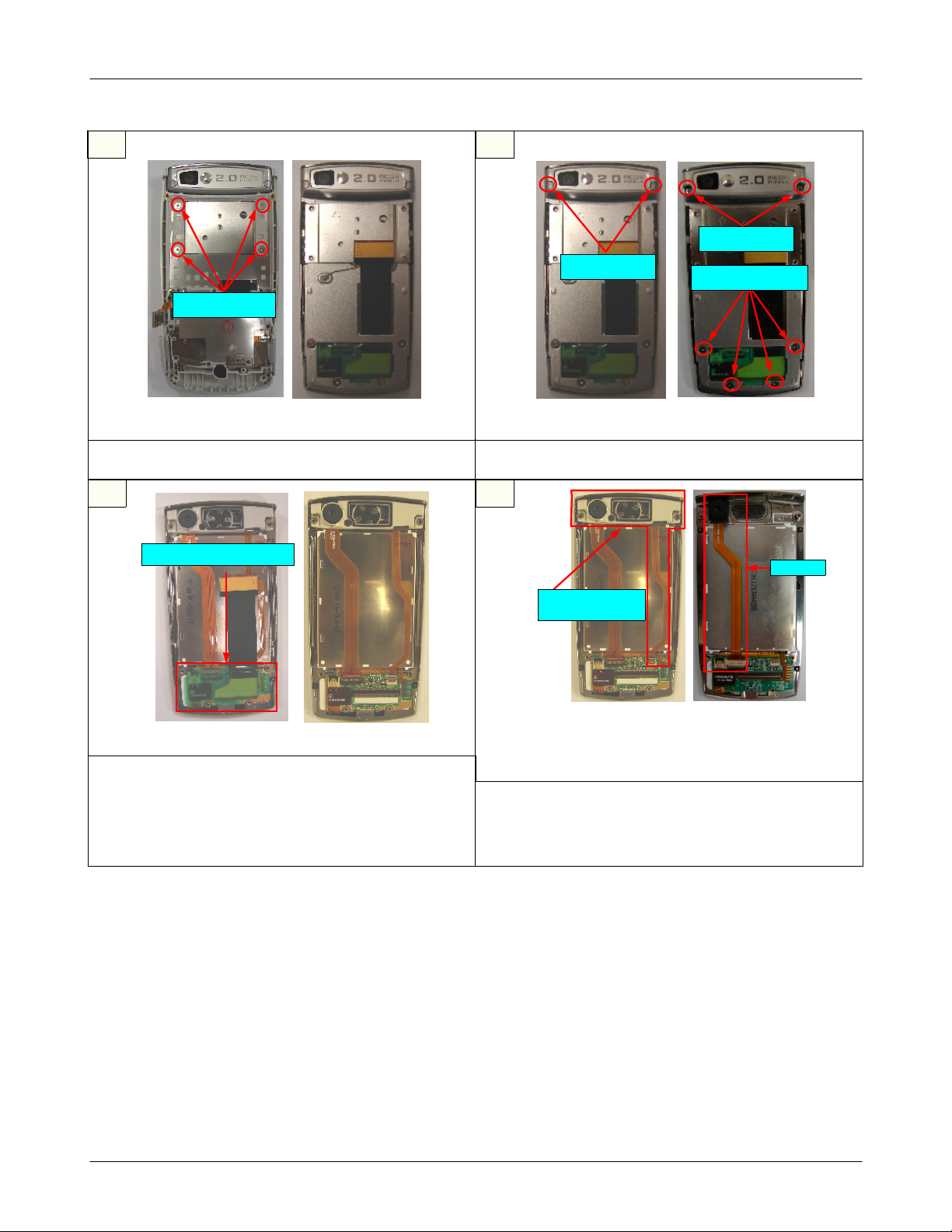
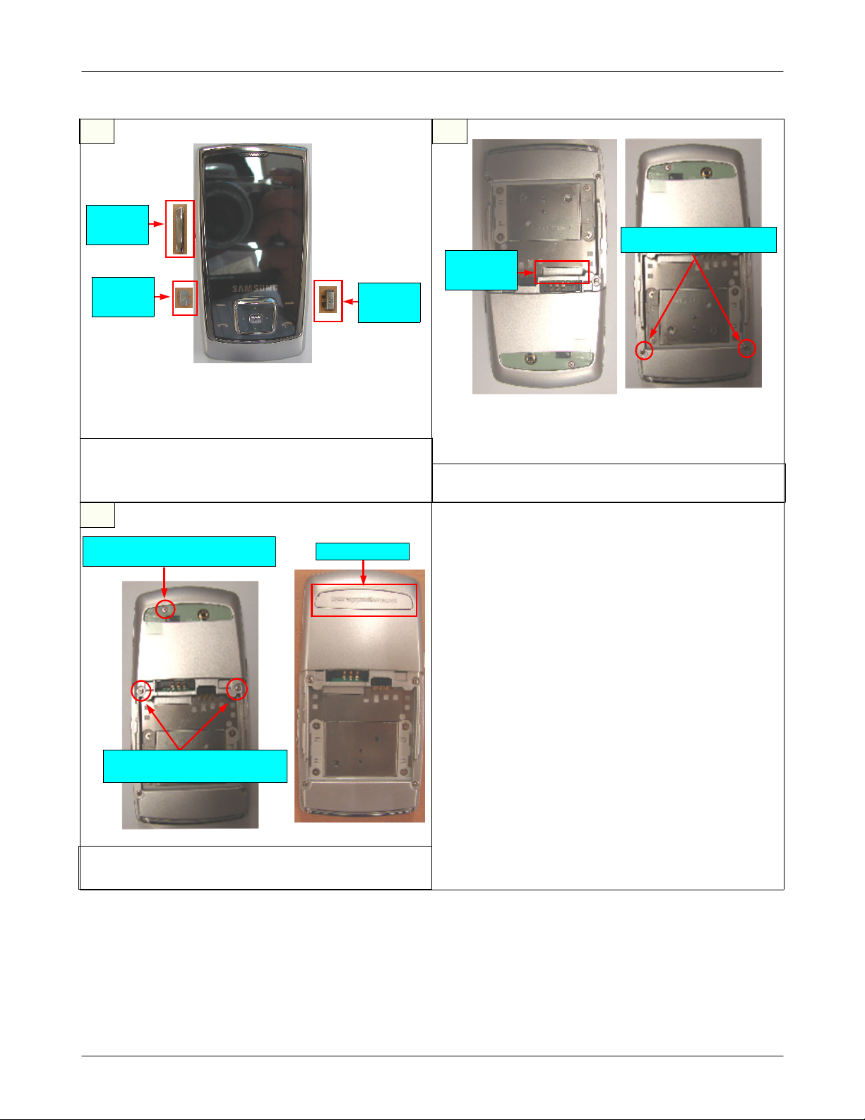
Disassembly
2-3.
Exploded View and Parts List
1
1) Detach from rear deco the back of a set with
2)
※
1)
Rear Deco
Screw(1.4*3)
Figure
<
tweezer.
Unscrew5points rear bolts the back of
set.[Figure
caution
Notice the Scratch on the Rear Cover when the
set disjoint.
[Figure 1]
1> <
2]
Screw(1.6*5)
Figure
2>
a
2
Figure
<
Screw A:1.4*3
<
Open the Micro SD Card Cover and Rear Cover
1)
with round tweezer.[Figure
Disjoint carefully Rear Cover shaking right and
2)
left[Figure
2]
1>
Screw B:1.4*4
Figure
2>
1]
Connector
Screw(1.4*4)
Figure
<
Detach the Connecter of
1)
Figure
[
Unscrew2points in intenna module.[Figure
2)
1> <
1]
Figure
key F-PCB.
3*4
2>
2]
43
F-PCB
Connector
Figure
<
Lift the intenna and PBA with tweezer.[Figure
1)
Detach the F-PCB.[Figure
2)
1> <
Figure
2]
2>
1]
2-5
SAMSUNG Proprietary-Contents may change without notice
This Document can not be used without Samsung's authorization
Exploded View and Parts List
5
Screw(1.4*1.1)
Figure
<
Unscrew4points Front Cover.[Figure
1)
Remove the Front Cover.[Figure
2)
Green insulated Tape
1>
<
Figure
2]
2>
1]
6
Screw(1.4*4)
Screw Cap
Figure
<
Remove the Screw cap2points[Figure
1)
Unscrew6points Slide Lower.[Figure
2)
1>
Screw(1.4*1.6)
Figure
<
87
Speaker
Module
2>
1]
2]
Camera
Figure
<
1>
Figure
<
1) Remove the Slide Lower.[Figure 1]
Detach the green
2)
insulated Tape and Pull out the
FPCB.[Figure 2]
caution
※
Detach the Green insulated tape carefully.
1)
2>
Figure
<
Detach the Speaker Module.[Figure
1)
Detach the Camera.[Figure
2)
caution
※
Notice the F-PCB so as not to damage.
1)
2-6
1>
2]
<
Figure
1]
2>
SAMSUNG Proprietary-Contents may change without notice
This Document can not be used without Samsung's authorization
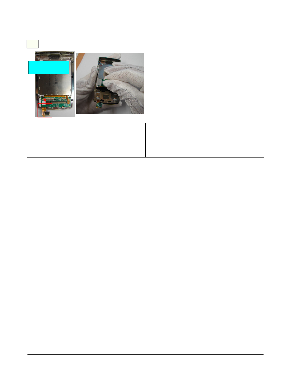
9
Touch Key
Connector
Pull out the Touch key connecter.
1)
Lift the LCD F-PCB and detach the LCD with
2)
Window.
caution
※
Be careful with the damage of LCD.
1)
[Figure 2]
[Figure 1]
Exploded View and Parts List
2-7
SAMSUNG Proprietary-Contents may change without notice
This Document can not be used without Samsung's authorization
Exploded View and Parts List
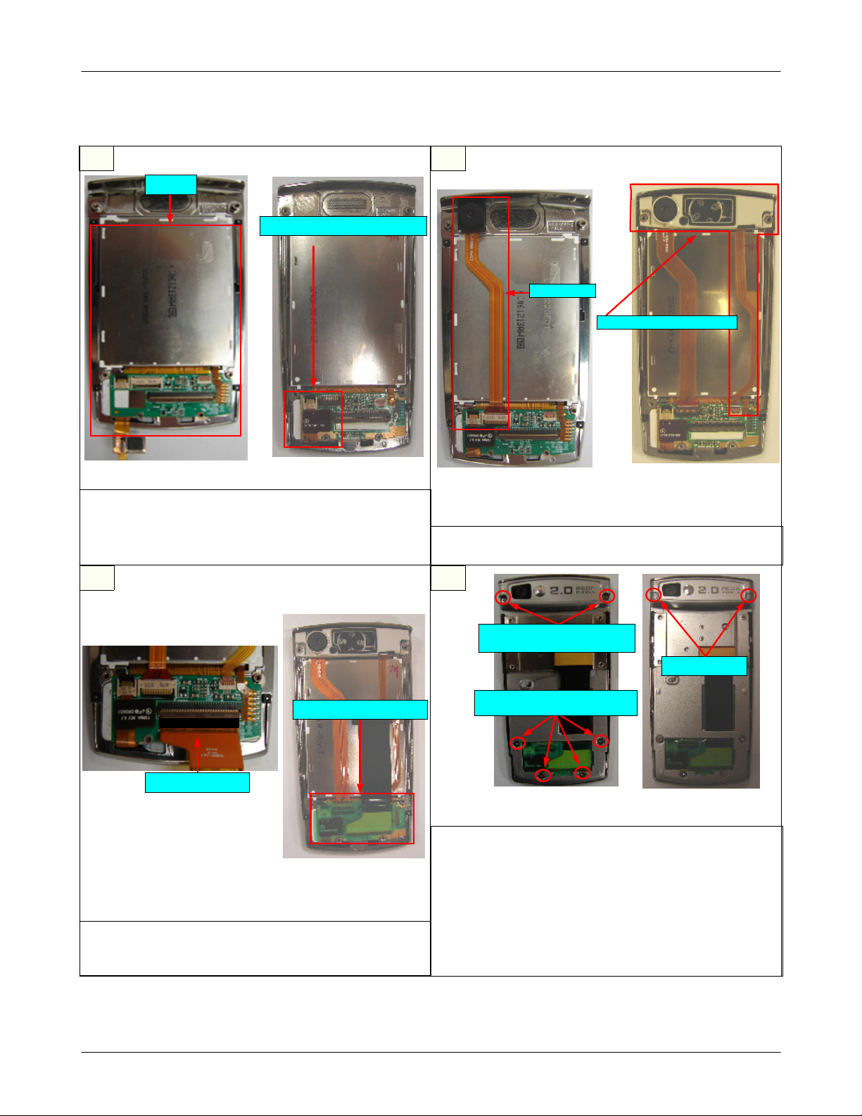
Assembly
2-4.
1
LCD
Touch Key Connector
Figure
<
Combine LCD Module.[Figure
1)
Insert the Touch Key F-PCB[Figure
2)
caution
※
Be careful of the possible damage on FPCB
1)
1>
1]
2]
<
Figure
2>
2
Camera
Speaker Modu le
Figure
<
Combine Camera module.[Figure
1)
Combine Speaker module.[Figure
2)
1>
<
Figure
1]
2]
2>
Green insulated Tape
both-sided Tape
Figure
<
1>
<
Fix the MIC in position like the picture.
1)
caution
※
Check the damage of F-PCB with an eye.
1)
Figure
2>
43
Screw(1.4*4)
Torque:1.2±0.1KgfㆍCm
Screw Cap
Screw(1.4*1.6)
Torque:1.0±0.1KgfㆍCm
Figure
<
Assemble the mic cover and then screw
1)
points.
2
Attach the KEY PAD.
2)
Press down the KEY PAD so as not to be
3)
detached it.
caution
※
Check the connecting condition of KEY PAD.
1)
1>
<
Figure
2>
2-8
SAMSUNG Proprietary-Contents may change without notice
This Document can not be used without Samsung's authorization
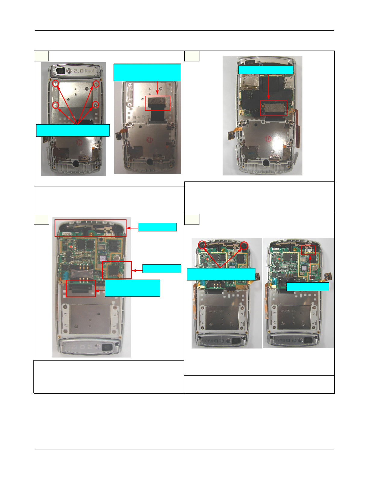
Exploded View and Parts List
5
Electric conduction
Sponge
Screw(1.4*1.1)
Torque:0.9±0.1KgfㆍCm
Figure
<
After combine Front Cover, the4Bolts
1)
Figure
[
Attach"electric conduction sponge" on connector.
2)
Figure
[
1]
2]
1>
<
Figure
2>
.
Intenna
6
F-PCB Connector
Insert"F-PCB" to the connector in PBA.
1)
caution
※
Connector should be certainly clicked along the
1)
marked line.
87
Connector
Flatten
by finger.
Insert
1)
Flatten F-PCB by finger while open and close
2)
key PCB" to the connector in PBA.
"3*4
slide.
Insert the Antenna module.
3)
Screw(1.4*4)
Torque:1.0±0.1KgfㆍCm
Soldering
Figure
<
1>
<
Figure
2>
1) Screw the 2 Bolts.[Figure 1]
2) As seen figure 2, soldering the antenna module.
2-9
SAMSUNG Proprietary-Contents may change without notice
This Document can not be used without Samsung's authorization
Exploded View and Parts List
9
Volume
Key
Power
Key
After combine Front Cover, the4Bolts
1)
Figure
[
Attach"electric conduction sponge" on connector.
2)
Figure
[
1]
2]
Camera
.
11
Screw(1.6*5)
Torque:1.0±0.1KgfㆍCm
Rear D eco
Key
10
Screw(1.4*3)
Camera
Key
Figure
<
1>
1) Push the parts, as seen Figure 1.
2) Screw the 2 Bolts, as seen above.[Figure 2]
Torque:1.3±0.1KgfㆍCm
Figure
<
2>
Screw(1.4*3)
Torque:1.0±0.1KgfㆍCm
1) Screw the 3 Bolts, as seen above. [Figure 1]
2) Attach the Rear Deco. [Figure 2]
SAMSUNG Proprietary-Contents may change without notice
This Document can not be used without Samsung's authorization
2-10

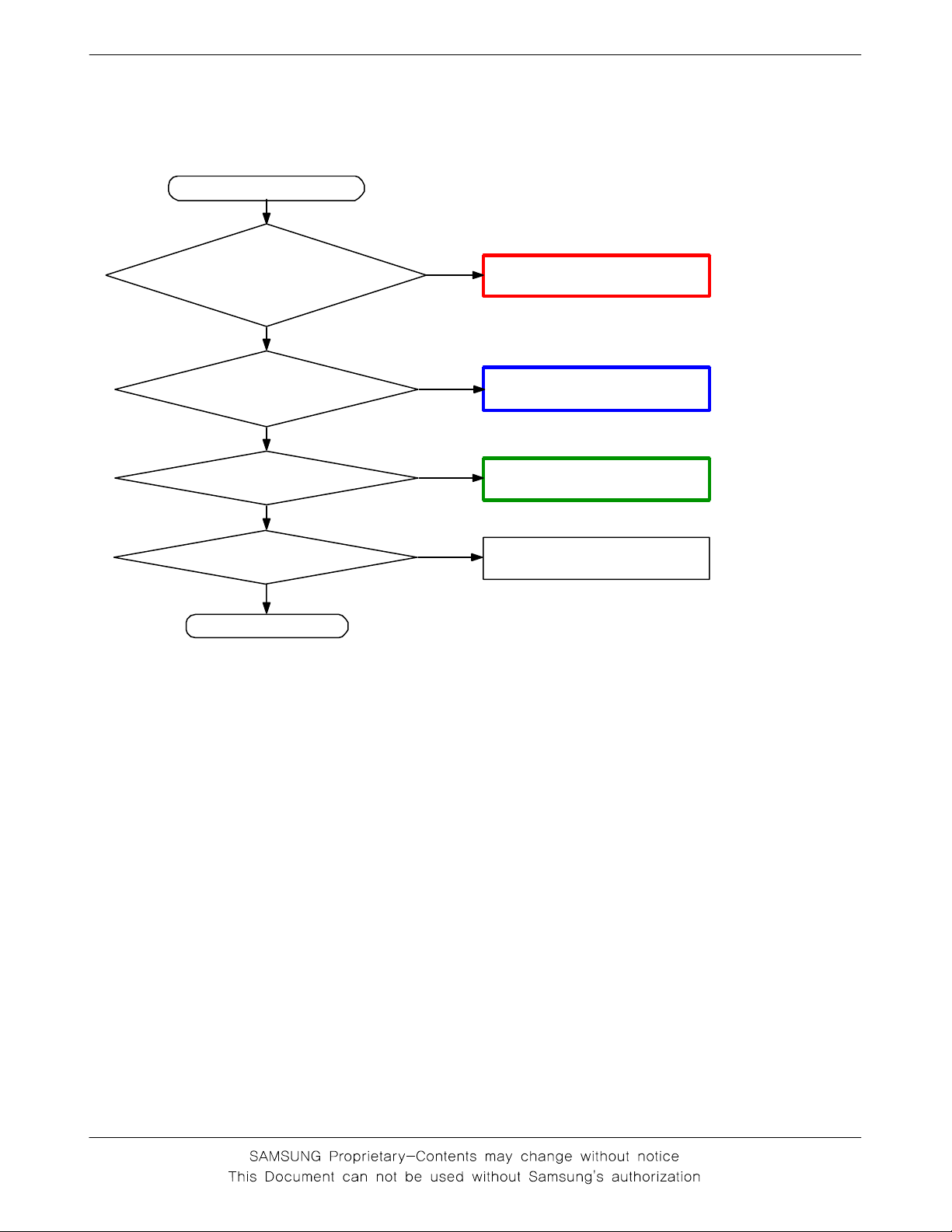
3. Flow Chart of Troubleshooting
BASEBAND
3-1
3-1-1.
Power ON
Power On' does not work
'
Yes
Check the current
consumption more
than
Check the VBAT
more than
VLDO7_1.8V
ofUCP
100
Yes
Yes
Check the
is more
300
than
1.8V
Yes
mA
3.3V
No
No
No
Download again
Charge the Battery
①
CheckUCP
300
and C31
5
Check U301
pin
1 = 1.8V
pin
4 = 1.6V
pin
7,9 = 1.5V
Yes
Check VRF of
UCP300=2.9V
Yes
Check
C130
Freq
Vp-p
Check the initial operation
=13
>0.8V
Yes
Yes
END
MHz
No
No
No
②
Check
③
CheckUCP
and C31
④
Check the clock C1
U301
300
6
30
3-1
Flow Chart of Troubleshooting
3-2
Flow Chart of Troubleshooting
1
1
3
C
V
5
.
1
_
C
T
R
V
0
3
3
C
9
0
3
C
T
A
B
V
0
1
C
3
1
7
0
3
V
9
.
2
_
D
C
C
V
V
8
.
1
_
D
C
C
V
V
9
.
2
_
A
C
C
V
V
9
.
2
_
F
R
V
C
6
0
3
C
8
0
3
C
5
0
3
C
B
8
E
5
1
B
5
1
K
1
1
F
3
J
3
M
6
N
5
N
4
J
5
G
4
K
2
R
6
P
1
1
N
0
1
M
6
A
6
F
1
1
L
3
1
P
4
C
4
B
3
1
D
7
F
8
F
9
F
0
1
F
7
G
8
G
9
G
0
1
G
6
H
7
H
8
H
9
H
7
J
8
J
9
J
0
1
J
1
K
0
1
2
K
C
E
H
C
_
R
A
E
)
5
1
:
0
(
B
D
_
P
S
D
A
T
T
K
L
A
S
C
D
R
M
M
M
I
I
I
S
S
S
1
0
0
3
1
9
1
1
1
C
N
J
P
R
4
2
T
K
O
I
3
1
S
L
_
D
D
R
C
P
D
D
_
_
U
V
V
P
P
U
U
5
D
D
V
7
6
D
D
V
Q
D
N
G
1
C
S
P
G
_
D
N
C
2
S
P
G
_
D
N
G
H
N
_
D
R
U
C
1
D
D
V
2
D
D
V
3
D
D
V
I
1
_
O
D
D
V
I
2
_
O
D
D
V
S
S
V
1
S
S
V
2
3
S
S
V
4
S
S
V
D
D
D
V
D
D
N
G
B
D
D
V
D
N
G
B
V
D
D
V
V
D
N
G
L
O
T
C
_
D
V
D
L
O
T
C
G
_
N
D
3
C
D
A
_
X
A
U
S
D
N
G
1
2
S
D
N
G
S
D
N
G
3
4
S
D
N
G
5
S
D
N
G
S
D
N
G
6
S
D
N
G
7
S
D
N
G
8
9
S
D
N
G
0
1
S
D
N
G
S
D
N
1
1
G
S
D
N
G
2
1
3
1
S
D
N
G
4
D
1
S
N
G
S
D
N
G
5
1
S
D
N
G
6
1
S
D
N
G
7
1
5
C
N
6
C
N
5
3
4
1
1
1
B
B
B
D
D
D
3
2
3
E
D
D
)
)
)
)
4
2
3
5
1
1
1
(
(
(
B
B
B
D
D
D
_
_
_
P
P
P
S
S
S
D
D
D
0
0
3
R
V
5
.
1
_
1
O
D
L
V
V
9
.
2
_
D
C
C
V
V
9
.
2
_
F
R
V
V
9
.
2
_
A
C
C
V
C
S
P
_
V
8
M
.
I
1
S
_
D
V
C
C
V
2
3
3
C
V
9
.
2
T
K
_
L
S
B
O
I
C
R
C
_
_
_
C
M
M
M
I
I
I
V
S
S
S
2
1
4
2
1
1
1
1
1
1
1
1
K
K
H
J
K
G
T
C
V
K
O
M
I
I
S
T
L
R
_
S
R
R
C
D
V
M
_
_
V
I
_
2
S
M
M
I
I
D
S
S
E
L
1
2
0
1
1
1
6
9
7
8
B
B
B
B
B
B
B
D
D
D
D
D
D
D
3
2
3
2
4
1
4
F
F
F
F
E
G
G
)
)
1
0
)
)
)
)
1
1
1
8
7
9
6
(
(
(
(
(
(
(
B
B
B
B
B
B
B
D
D
D
D
D
D
D
_
_
_
_
_
_
_
P
P
P
P
P
P
P
S
S
S
S
S
S
S
D
D
D
D
D
D
D
)
8
:
0
(
B
A
_
P
S
D
0
1
3
C
N
I
A
M
_
L
B
_
Y
E
K
3
0
2
0
4
5
3
1
1
9
1
1
1
1
1
F
D
F
A
B
C
C
G
V
R
D
_
1
D
E
L
5
B
D
5
H
)
5
(
B
D
_
P
S
D
5
6
7
V
V
A
B
_
_
_
_
_
R
R
O
O
O
S
S
D
D
5
5
_
D
D
D
_
L
L
L
L
L
B
G
I
V
V
V
V
V
N
V
I
R
0
0
3
P
C
U
0
1
2
3
4
8
7
B
B
B
B
B
B
B
A
A
D
D
D
D
D
5
7
1
2
5
6
3
J
J
K
K
K
K
K
)
)
)
)
)
0
4
3
2
1
(
(
(
(
(
B
B
B
B
B
)
)
D
D
D
D
D
8
7
_
_
_
_
_
(
(
P
P
P
P
P
B
B
S
S
S
S
S
A
A
_
_
D
D
D
D
D
P
P
S
S
D
D
0
0
3
T
A
B
2
1
G
S
O
P
2
1
3
C
N
N
E
E
_
_
X
X
T
T
_
_
S
M
S
C
D
G
2
1
1
1
A
B
A
B
_
_
S
S
4
4
L
L
V
V
5
6
B
B
A
A
2
1
M
M
)
)
5
6
(
(
B
B
A
A
_
_
P
P
S
S
D
D
T
A
B
V
1
3
2
4
2
1
8
1
1
1
1
K
G
J
A
B
F
4
1
2
3
C
C
_
_
_
_
S
C
O
O
O
O
P
A
_
D
D
D
D
V
L
L
L
L
N
V
V
V
V
S
C
N
3
4
2
1
0
W
B
B
B
B
B
O
|
A
A
A
A
A
I
R
1
2
1
5
6
2
3
L
L
L
P
N
N
K
)
)
)
)
)
4
2
3
1
0
(
(
(
(
(
B
B
B
B
B
A
A
A
A
A
_
_
_
_
_
P
P
P
P
P
S
S
S
S
S
D
D
D
D
D
O
I
_
P
S
D
V
9
.
2
_
E
N
B
C
C
V
9
1
3
C
8
1
3
C
7
1
3
C
6
1
3
C
4
1
3
C
5
1
3
C
K
L
I
O
S
C
D
D
S
S
S
C
_
_
_
_
P
P
P
P
U
U
U
U
4
1
3
2
7
7
1
1
1
8
L
C
S
P
_
K
L
C
S
P
S
C
_
N
T
E
S
E
R
3
R
N
W
R
_
P
S
D
1
N
M
E
E
F
E
T
C
C
N
V
T
X
S
S
E
A
R
E
P
P
S
B
D
I
V
_
_
V
B
I
_
O
_
D
H
D
H
S
C
S
C
1
0
2
4
3
5
L
L
L
L
L
L
T
T
T
T
T
T
C
C
C
C
C
C
O
O
O
O
O
O
6
5
5
5
6
4
F
E
E
C
A
G
L
N
L
A
N
T
E
E
E
E
E
N
_
S
_
S
S
E
_
X
_
X
E
O
D
T
S
D
R
X
O
_
N
A
H
M
B
S
A
L
F
0
2
3
C
5
0
0
0
3
3
R
R
V
6
0
3
R
2
2
3
C
M
R
A
L
G
A
R
C
H
T
C
R
I
7
0
3
R
1
2
3
4
5
0
0
1
1
1
1
D
E
A
D
F
S
1
2
E
E
X
X
R
R
U
U
_
V
A
A
_
_
H
C
C
C
N
D
D
A
A
2
1
6
7
E
E
L
L
L
L
T
T
R
R
C
C
E
E
S
S
O
O
1
2
1
3
3
A
B
C
B
A
N
E
N
L
E
E
_
_
R
X
E
C
R
S
A
P
C
0
1
9
E
H
F
N
E
M
R
L
C
A
_
C
E
N
R
_
I
V
G
_
B
L
9
T
R
I
T
N
Q
R
0
L
1
K
P
E
W
E
_
R
P
M
9
E
D
M
O
0
N
1
E
S
E
R
O
_
T
K
9
B
F
U
_
W
1
S
P
L
7
N
S
W
W
1
_
R
P
5
C
1
S
W
W
2
_
R
P
4
C
1
R
I
D
T
N
P
3
A
4
X
U
_
C
D
A
P
5
M
C
R
6
A
Q
N
O
E
X
1
D
K
L
C
_
C
T
R
N
4
I
A
D
O
D
M
6
I
A
D
I
D
L
6
I
A
D
N
R
P
4
I
A
D
K
C
R
4
N
G
E
R
V
4
R
1
P
G
E
R
V
M
3
1
M
C
V
X
V
3
R
1
U
N
O
T
X
U
A
3
L
1
U
P
O
T
X
U
A
3
K
1
I
X
U
A
N
N
4
L
1
I
X
U
A
P
N
M
5
1
M
I
N
O
C
T
U
5
P
1
M
I
P
O
C
T
U
5
N
1
M
I
I
C
N
N
M
4
1
M
I
I
C
P
N
4
N
1
B
T
N
O
A
U
2
P
1
B
T
P
O
A
U
2
R
1
A
T
N
O
A
U
2
N
1
A
T
P
O
A
U
1
P
1
N
Q
X
T
X
R
C
6
P
Q
X
T
X
R
C
7
I
X
N
T
X
R
D
6
I
X
P
T
X
R
D
7
F
1
E
R
A
R
B
6
F
2
E
R
A
R
B
5
P
X
T
E
7
C
F
A
D
9
A
K
D
C
R
R
E
E
S
S
2
C
T
K
L
A
C
D
R
R
E
E
S
S
P
E
E
K
_
Q
R
R
T
T
S
W
N
R
I
P
T
A
B
V
1
F
_
W
U
S
B
P
P
R
O
W
_
N
J
I
G
O
_
N
T
D
I
N
_PS
C
L
1
3
_
K
C
M
M
O
X
E
A
N
Q
3
KLC
2
K
4
2
3
C
U
O
T
A
X
U
N
A
U
O
T
X
U
P
U
A
X
I
N
N
I
A
N
X
U
P
I
C
M
N
O
T
U
O
I
T
C
U
M
P
I
C
N
M
I
N
I
I
C
N
M
P
O
A
U
B
T
N
A
U
B
O
T
P
O
A
U
A
T
N
A
U
A
O
T
P
Q
XTR
N
Q
XTR
P
I
N
X
T
R
R
X
T
I
P
V
P
A
C
3
F
A
C
2
3
C
3-3
Flow Chart of Troubleshooting
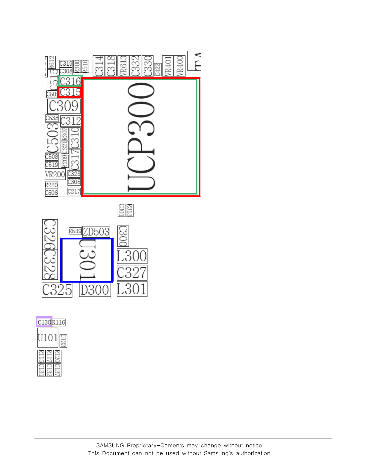
C130
13M_BUF
1
2
3
NC
A
GND
U101
R116
VCC
NC
5
4
Y
VRF_2.9V
6
C133
R115
R117
R120
C131
C132
C137
HP_CORE_1.575V
CLK13M_TR
CLK13M_MC
CLK13M_YMU
VLDO1_1.5V
10
9
8
7
6
SW2
EN2
GND
EN1
SW1
D300
L300
U301
ADJ2
MODE|DATA
VIN
2
FB1
D
N
DEF_1
G
11
L301
VCCD_1.8V
1
2
3
4
5
C326
C327
C325
VBAT
C328
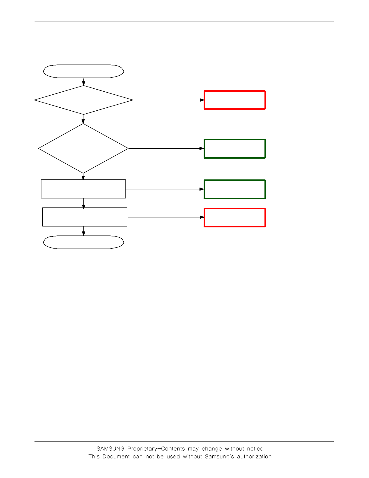
3-4
Flow Chart of Troubleshooting
3-1-2.
Initial
Initial Failure
Check VCCD,
VCCD_1.8V of UCP300
"High" when the phone
is boot on`
Check the
HP_CORE_1.575V of
U201 is "High"
LCD display is O.K?
Sound is O.K?
Yes
Yes
Yes
Yes
No
No
No
No
①
Check UCP300
②
Chec k U301
③
Chec k HDC602 an d LCD part
Chec k aud io par t
END
Yes
3-5
Flow Chart of Troubleshooting
VMOT_3.3V
VCAM_2.8AV
VCCD_2.9V
VCAM_2.8DV
VTOUCH_3.1V
HDC602
1
2
1
2
4
3
4
TOUCH_RST
SCL_TOUCH_M
LCD_ADS_O
LCD_WEN_O
LCD_DO(0) LCD_DO(1)
LCD_DO(2) LCD_DO(3)
LCD_DO(4) LCD_DO(5)
LCD_DO(6) LCD_DO(7)
LCD_DO(8) LCD_DO(9)
LCD_DO(10) LCD_DO(11)
LCD_DO(12) LCD_DO(13)
LCD_DO(14) LCD_DO(15)
LED_A
LED_4 LED_3
LED_2 LED_1
CAM_D(0) CAM_D(1)
CAM_D(2)
CAM_D(4) CAM_D(5)
CAM_D(6) CAM_D(7)
CAM_VSYNC
CAM_HSYNC
C_SCL
CAM_RST
SPK_P_CON
2
3
1
1
6
6
R
R
V
V
3
5
6
5
7
78
9
10
9
11
11 12
13
13 14
15
15 16
17
17 18
19
20
19
21
21 22
23
23 24
25 26
25
26
27
27
28
29
29
30
31
31 32
33
33 34
35
35 36
37
37 38
39
39
40
41
42
41
43 44
43
44
45 46
45
46
47 48
47
48
49
50
49
51 52
51
52
53 54
53
54
55 56
55
56
57 58
57
58
59
59
60
C
C
C
C
N
N
N
N
1
3
4
2
6
6
6
6
6
8
10
12
14
16
18
20
22
24
28
30
32
34
36
38
40
42
50
60
R647
VCAM_1.5V
R648
R649
TOUCH_IRQ
SDA_TOUCH_M
LCD_FLM_2.9V
MLCD_CS_O
LCD_RD
LED_5
CAM_D(3)
M_CLK
P_CLK
C_SDA
SPK_N_CON
3-6
LCD_SW_RESET
VCCD_2.9V
R612
C615
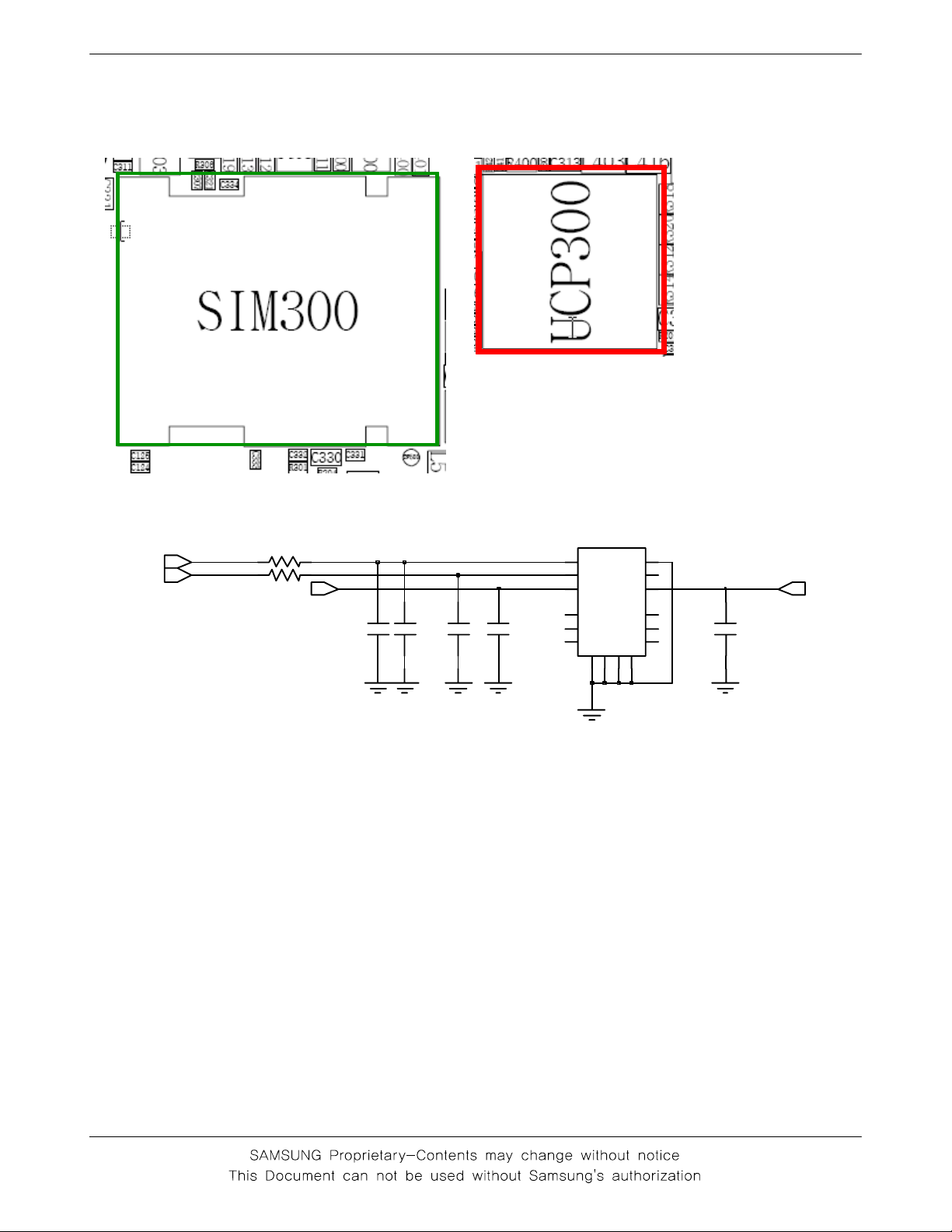
Flow Chart of Troubleshooting
3-1-3.
Sim Part
Phone can't access
SIM card
Check the pin 1 of
SIM300
Volt ag e = 3V
YES
Check the SIM
connec tor' s
(S IM30 0)
connec tor' s to SIM
card
YES
Check the circui t around SIM30 0
input circuitry
YES
Check the ci rcui t around
UCP3 00 output
and voltage supply circuitry
YES
NO
NO
NO
NO
①
Check the circuit related to
UCP300
②
resolder or change
SIM300
③
Check the relate d circuit of
SIM3 00
④
Check the relate d circuit of
UCP300
END
3-7
Flow Chart of Troubleshooting
VSIM
SIM_RST
R313
R314
SIM_CLK
C300
C301
C302 C303
SIM300
11
22
33
7
7
88
99
G
1415GG16
6
5
4
12 12
10 10
G
13
6
5
4
1111
SIM_IO
C304
3-8
 Loading...