

Samsung SGH-E750 Service Manual
GSM TELEPHONE
SGH-E750
GSM TELEPHONE
CONTENTS
1. Specification
2. Circuit Description
3. Exploded Views and Parts List
4. Electrical Parts List
5. Block Diagrams
6. PCB Diagrams
7. Flow Chart of Troubleshooting
This Service Manual is a property of Samsung Electronics Co.,Ltd.
Any unauthorized use of Manual can be punished under applicable
International and/or domestic law.
ⓒ
Samsung Electronics Co.,Ltd. September. 2005
Printed in Korea.
Code No.: GH68-08355A
BASIC.
1. Specification
1-1. GSM General Specification
GSM900
Phase 1
Freq. Band[MHz]
Uplink/Downlink
ARFCN range 1~124
Tx/Rx spacing 45MHz 45MHz 95MHz 80MHz
Mod. Bit rate
/BitPeriod
Time Slot Period
/FramePeriod
Modulation 0.3GMSK 0.3GMSK 0.3GMSK 0.3GMSK
MS Power 33dBm~13dBm 33dBm~5dBm 30dBm~0dBm 30dBm~0dBm
890~915
935~960
270.833kbps
3.692us
576.9us
4.615ms
EGSM 900
Phase 2
880~915
925~960
0~124 &
975~1023
270.833kbps
3.692us
576.9us
4.615ms
DCS1800
Phase 1
1710~1785
1805~1880
512~885 512~810
270.833kbps
3.692us
576.9us
4.615ms
PCS1900
1850~1910
1930~1990
270.833kbps
3.692us
576.9us
4.615ms
Power Class 5pcl ~ 15pcl 5pcl ~ 19pcl 0pcl ~ 15pcl 0pcl ~ 15pcl
Sensitivity -102dBm -102dBm -100dBm -100dBm
TDMA Mux 8 8 8 8
Cell Radius 35Km 35Km 2Km -
1-1
SAMSUNG Proprietary-Contents may change without notice
This Document can not be used without Samsung's authorization
Specification
1-2. GSM TX power class
TX Power
control level
5 33±3 dBm
6 31±3 dBm
7 29±3 dBm
8 27±3 dBm
9 25±3 dBm
10 23±3 dBm
11 21±3 dBm
GSM900
TX Power
control level
0 30±3 dBm
1 28±3 dBm
2 26±3 dBm
3 24±3 dBm
4 22±3 dBm
5 20±3 dBm
6 18±3 dBm
DCS1800
TX Power
control level
0 30±3 dBm
1 28±3 dBm
2 26±3 dBm
3 24±3 dBm
4 22±3 dBm
5 20±3 dBm
6 18±3 dBm
PCS1900
12 19±3 dBm
13 17±3 dBm
14 15±3 dBm
15 13±3 dBm
16 11±5 dBm
17 9±5 dBm
18 7±5 dBm
19 5±5 dBm
7 16±3 dBm
8 14±3 dBm
9 12±4 dBm
10 10±4 dBm
11 8±4dBm
12 6±4 dBm
13 4±4 dBm
14 2±5 dBm
7 16±3 dBm
8 14±3 dBm
9 12±4 dBm
10 10±4 dBm
11 8±4dBm
12 6±4 dBm
13 4±4 dBm
14 2±5 dBm
15 0±5 dBm
1-2
15 0±5 dBm
SAMSUNG Proprietary-Contents may change without notice
This Document can not be used without Samsung's authorization
2. Circuit Description
2-1. SGH-E750 RF Circuit Description
2-1-1. RX PART
- FEM(MODULE100)→Switching Tx, Rx path for GSM900, DCS1800 and PCS1900 by logic controlling.
- FEM Control Logic (MODULE100)→Truth Table
VC1 VC2 VC3
Tx Mode (GSM900) H L L
Tx Mode (DCS1800/1900) L H L(H)
Rx Mode (GSM900) L L L
Rx Mode (DCS1800) L L L
Rx Mode (PCS1900) L L H
- VC-TCXO-2146C6(26MHz) (OSC100)
This module generates the 26MHz reference clock to drive the logic and RF.
It is turned on when the supply voltage is applied.
After buffering a reference clock of 26MHz is supplied to the other parts of the system through the transceiver pin
VCXOOUT1.
- Transceiver (U100)
This chip is a RF transceiver IC for GSM850/900, DCS1800, and PCS1900 Quad band cellular system, and incorporates
GPRS transceiver capability, and integrates most of the low power silicon functions of a transceiver.
It incorporates triple RF LNAs, direct conversion mixers which are IQ demodulator, an auto offset calibrated
programmable gain amplifier with baseband filter for IQ chains, RF synthesizer, a I/Q modulator, offset PLL, IF
synthesizer, and the circuits which are needed polar loop architecture for the transmitter.
2-1-2. TX PART
Transmitter of the transceiver is capable of GMSK and 8-PSK modulation, providing support for conventional GSM and
GPRS. The modulated signal out of the transceiver is fed into Power Amplifer Module(U101). PAM output signal is
radiated to the air through FEM(MODULE1) and antenna.
2-1
SAMSUNG Proprietary-Contents may change without notice
This Document can not be used without Samsung's authorization

Circuit Description
2-2. Baseband Circuit description of SGH-E750
2-2-1. PCF50603 (U405)
- Power Management
Eight low-dropout regulators designed specifically for GSM applications power the terminal and help ensure optimal
system performance and long battery life. A programmable boost converter provides support for 1.8V, 3.0V SIMs,
while a self-resetting, electronically fused switch supplies power to external accessories.
Ancillary support functions, such as RTC module and High Voltage Charge pump, Clock generator, aid in reducing
both board area and system complexity.
I2C BUS serial interface provides access to control and configuration registers. This interface gives a microprocessor
full control of the PCF50603 and enables system designers to maximize both standby and talk times.
Supervisory functions. including a reset generator, an input voltage monitor, and a temperature sensor, support reliable
system design. These functions work together to ensure proper system behavior during start-up or in the event of a
fault condition(low microprocessor voltage, insufficient battery energy, or excessive die temperature).
- Backlight Brightness Modulator
The Backlight Brightness Modulator (BBM) contains a programmable Pulse-width modulator (PWM) and FET to
modulate the intensity of a series of LED’ s or to control a DC/DC converter that drives LCD backlight.
- Clock Generator
The Clock Generator (CG) generates all clocks for internal and external usage. The 32.768 kHz crystal oscillator
provides an accurate low clock frequency for the PCF50603 and other circuitry.
2-2-2. LCD Connector
LCD is consisted of main MAIN LCD, SUB LCD
Chip select signals in the U305, LCD_CS, can enable LCD. BACKLIGHT signal enables white LED of main LCD. These
signal is from U400.
16-bit data lines(LD(0)~LD(15)) transfers data and commands to LCD. Data and commands use "RS" signal. If this signal
is high, Inputs to LCD are commands. If it is low, Inputs to LCD are data. The signal which informs the input or output
state to LCD, is required. But this system is not necessary this signal. So "L_WR" signal is used to write data or
commands to LCD. Power signals for LCD are "VDD_IO_HIGH".
2-2-3. Key
This is consisted of key interface pins KEY_ROW(0:4) and KEY_COL(0:4) in PCF5213EL1. These signals compose the
matrix. Result of matrix informs the key status to key interface in the PCF5213EL1. Power on/off key is seperated from
the matrix. So power on/off signal is connected with PCF50603 to enable PCF50603. Key LED is consisted of six white
LEDs for sub key and eight white LEDs for main key.
Main and Sub key LED use the 3.3V LDO for a supply voltage. KEY_LED_ON signal enables eight white LED.
2-2
SAMSUNG Proprietary-Contents may change without notice
This Document can not be used without Samsung's authorization

Circuit Description
2-2-4. EMI ESD Filter
This system uses the EMI ESD filter, U500 to protect noise from IF CONNECTOR part.
2-2-5. IF connetor
It is 18-pin connector. They are designed to use VBAT, V_EXT_CHARGE, USB_D+, +VBUS, USB_D-, TXD1, RXD1,
AUX_ON, EXT1, EXT2 and GND. They connected to power supply IC, microprocessor and signal processor IC.
2-2-6. Battery Charge Management
A complete constant-current/constant-voltage linear charger for single cell lithium-ion batteries.
If TA connected to phone, "V_EXT_CHARGE" enable charger IC and supply current to battery.
When fault condition caused, "CHG_ON" signal level change low to high and charger IC stop charging process.
2-2-7. Audio
HFR_P and HFR_N from PCF5213EL1 are connected to the main speaker via analog switches. MIC_P and MIC_N
are connected to the main MIC as well. YMU765 is a synthesizer LSI for mobile phones. This LSI has a built-in speaker
amplifier for outputting sounds that are used by mobile phones in addition to game sounds and ringing melodies that are
replayed by a synthesizer.
There is Stereophonic analog output for Headphone.
2-2-8. Memory
This system uses Samsung's memory,
Memory whichcombines 256Mbit Synchronous Burst Multi Bank NOR Flash Memory and 1Gbit NAND
Flash and 128Mbit Synchronous Burst U tRAM.
It has 16 bit data line, HD[1~16] which is connected to PCF5213 and MV3315DOQ, also has 24 bit address lines,
HA[1~24]. There are 3 chip select signals, CS0n_FLASH, CS4n_NAND, and CS1n_RAM.
In the Wrting process, WEn is fallen to low and it enables writing process to operate. During reading process,
OEn is fallen to low and it enables reading process to operate. Each chip select signals in the PCF5213EL1 choose
different memories.
KBJ10KB00A
.The
KBJ10KB00A
. is a Multi Chip Package
2-2-9. PCF5213EL1
The PCF5213EL1 is mainly composed of embeded DSP and ARM core. The DSP subsystem includes the Saturn
DSP core with embedded RAM and ROM, and a set of peripherals. It has 24kx16 bits PRAM, 104k*16 bits,
32k*16 XYRAM and 63k*16 XYROM in the DSP.
The ARM946E-S consists of an ARM9E-S processor core, 8 kbyte instruction cache and 8 kbyte data cache,
tghtly-coupled ITCM(Instruction Tightly Coupled Memory) and DTCM(Data Tightly Coupled Memory) memories, a
memory protection unit, and an AMBA(Advanced Microcontroller Bus Architecture) AHB(Advanced
High-performance Bus) bus interface with a write buffer.
HD(0:15), data lines and HA(0:23), address lines are connected to KBJ10KB00M (memory), MV319DNQ (image dsp)
and YMU765 (melody IC). It has 64 kbyte SC RAM (0.5 Mbit) and 32 kbyte SC program ROM for bootstrap
loader in the ARM core.
2-3
SAMSUNG Proprietary-Contents may change without notice
This Document can not be used without Samsung's authorization

Circuit Description
HD(0:15), data lines and HA(0:23), address lines are connected to memory and YMU765 to communicate.
MV319DNQ(Camera DSP Chip) controls the communication between ARM core and DSP core.
OEn, WEn control the access of memory. KROW, and KCOL recognize the key string input status.
It has J-TAG control pins (TDI/TDO/TCK) for ARM and DSP core. J-SEL signal controls different access to ARM
and DSP core.
ADC(Analog to Digital Convertor) receives the condition of temperature, battery type and battery voltage.
2-2-10. TOH2600DGI4KRA(26MHz)
This system uses the 26MHz TCXO, VC-TCXO-214C6.AFC control signal form PCF5213EL1 controls requency from
26MHz x-tal. It generates the clock frequency. This clock is connected to PCF5213EL1, YMU765 and
MV3315DOQ.
2-2-11. Camera DSP(MV3315DOQ)
MV3315DOQ provides rich video functions up to 30-frame display with minimized tasks in the handset main processor
as well as hardware based real-time JPEG compression and decompression. MV3315DOQ directly transmits and
previews the RGB data to the LCD graphic memory by processing the sensor output data according to the
handset's command. It can save the raw RGB data up to VGA resoultion into its image buffer and allows the
host processor to download with scalable sized compressed data.
It utilizes 16 bit data bus for communication with the main processor, including bus interface types.
2-2-12. KXP74
KXP74 is Tri-axis Orthogonal accelerometers and inclinometers.
The KXP74 utilizes an onboard Serial Peripheral Interface (SPI) for digital communication.
PCF5213EL1 apply KXP74 for G- button and game
2-4
SAMSUNG Proprietary-Contents may change without notice
This Document can not be used without Samsung's authorization
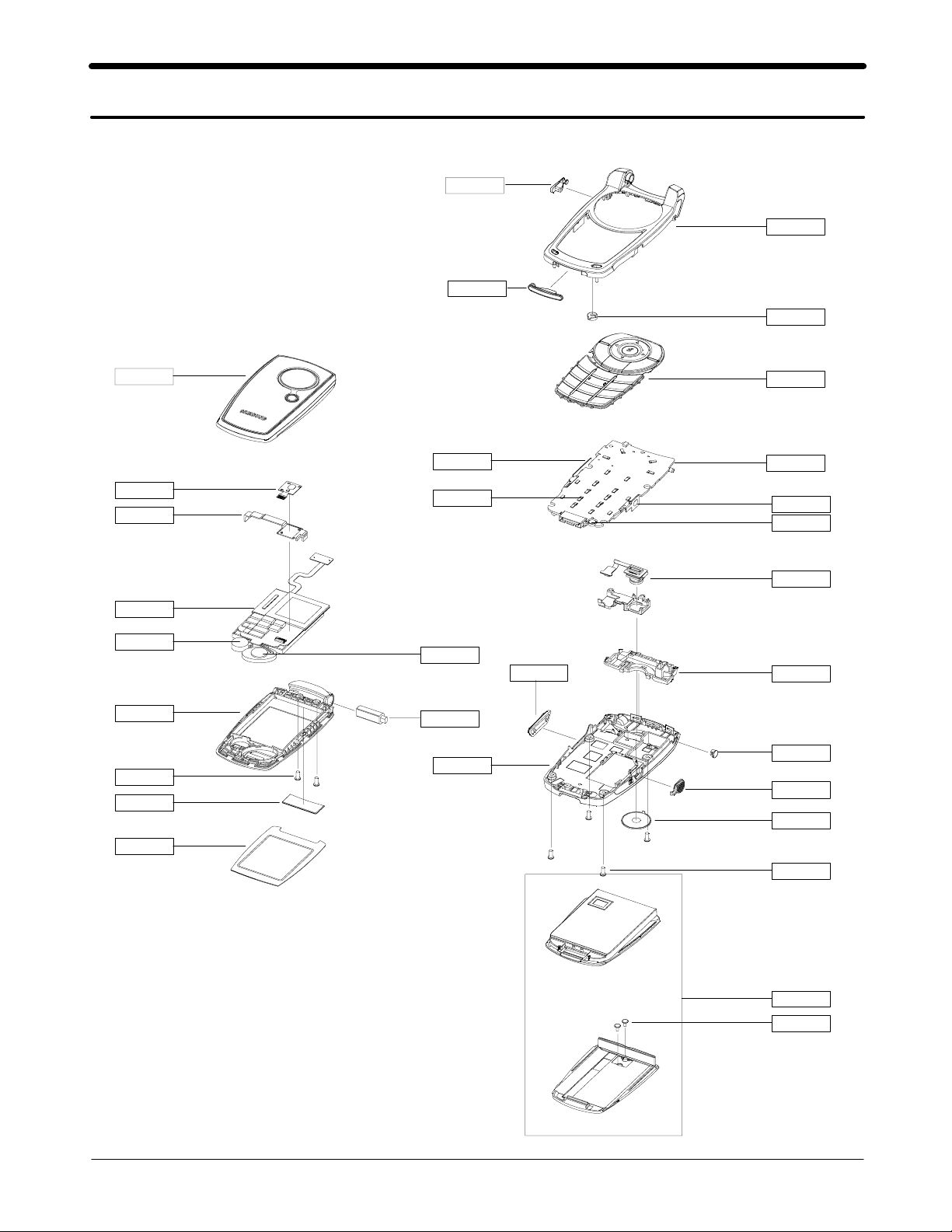
3. Exploded View and Parts List
3-1. Exploded View
QRF03
QFR01
QIF01
QMI03
QFU01
QME03
QVO08
QLC01
QMO01
QFL01
QCR06
QSC14
QMW02
QVK01
QME01
QSP01
QHI01
QRE01
QVO01
QKP01
QMP01
QCA02
QMI01
QCA01
QAN02
QRF01
QCK01
QCW01
QCR07
3-1
SAMSUNG Proprietary-Contents may change without notice
This Document can not be used without Samsung's authorization
QBA01
QCR06
Exploded view and Part List
3-2. Parts List
Location No Description Sec Code
QAN02
QBA01
QCA01
QCA02
QCK01
QCR06
QCR07
QFU01
QKP01
QLC01
QME01
QME03
QMI01
QMO01
QMP01
QMW02
QRF01
QSC14
QSP01
QVK01
QVO01
QVO08
QFR01
ㅤ
ㅤ
ㅤ
QFL01
ㅤ
QRE01
ㅤ
ㅤ
ㅤ
ㅤ
ㅤ
ㅤ
ㅤ
ㅤ
ㅤ
ㅤ
ㅤ
ㅤ
ㅤ
ㅤ
ㅤ
ㅤ
ㅤ
ㅤ
ㅤ
ㅤ
ㅤ
ㅤ
ㅤ
ㅤ
QIF01 PMO-IF COVER;SGH-E750,URETHANE+PC(K2 GH72-22315A
QRF03 PMO-EAR COVER;SGH-E750,URETHANE+PC(K GH72-22316A
QMI03 RMO-MIC HOLDER;SGH-E750,SLICON RUBBE GH73-05134A
ㅤ
QHI01 MEC-HINGE;SCH-S400,SKT,-,-,-,-,-,- GH75-07998A
ㅤ
QCW01 MEC-CAMERA DECO;SGH-E750,EU,-,-,-,-, GH75-07646A
INTENNA-SGHE750;IGT-0061,SGH-E750,18 GH42-00633A
BATTERY-1000MAH,SIL,EU,M;BST4468SE,S GH43-01986A
UNIT-CAMERA;SPH-E750,MOMFH342G1A,-,E GH59-02258A
UNIT-CAMERA KEY;SGH-E750,-,-,EU,5V,1 GH59-02232A
MEC-CAMERA KEY;SGH-E750,EU,-,-,-,-,W GH75-08044A
SCREW-MACHINE;PH(PI2.5),+,M1.4,L3.5, 6001-001155
SCREW-MACHINE;CH,+,M1.7,L4,ZPC(BLK), 6001-001691
MEC-FOLDER UPPER;SGH-E750,EU,-,-,-,- GH75-07644A
MEC-KEYPAD(SER);SGH-E750,SER,-,-,-,- GH75-07651A
LCD-SGHE750 MODULE;UF-17E107-A,SGH-E GH07-00760A
UNIT-METAL DOME;SGH-E750,-,-,EU,3.5V GH59-02331A
UNIT-KEY FPCB;SGH-E750,YWCE750,-,EU, GH59-02280A
MICROPHONE-ASSY-SGHE750;2,130~500uA, GH30-00207A
MOTOR DC-SGHZ130;DMJBRK20NZ,SGH-Z130 GH31-00153J
PBA MAIN-SGHE750;SGH-E750,XET,EU,PBA GH92-02273A
PCT-MAIN WINDOW;SGH-E750,ACRYL,TRP,- GH72-22356A
PMO-RF COVER;SGH-E750,URETHANE+PC(K2 GH72-22324A
PMO-FOLDER SCREW COVER;SGH-E750,POLY GH72-24658A
SPEAKER;0.8W,8ohm,89B±2dB,800Hz,19. 3001-001795
UNIT-VOLUME KEY;SGH-E750,-,-,EU,5V,1 GH59-02231A
MEC-VOLUME KEY;SGH-E750,EU,-,-,-,-,W GH75-07962A
NDC-KEY MODE BRACKET;-,SGH-E750,ZN D GH71-05082A
MEC-FRONT COVER;SGH-E750,EU,-,-,-,-, GH75-07641A
MEC-FOLDER LOWER;SGH-E750,EU,-,-,-,- GH75-07643A
MEC-REAR COVER;SGH-E750,EU,-,-,-,-,B GH75-07642A
3-2
SAMSUNG Proprietary-Contents may change without notice
This Document can not be used without Samsung's authorization
Exploded view and Part List
Description Sec Code
BAG PE;LDPE,T0.05,W80,L180,TRP,-,- 6902-000634
CBF INTERFACE-DATA LINK CABLE;SGH-D5 GH39-00371A
ADAPTOR-SGHD500 BLK;TAD137EBE,SGH-D5 GH44-00954A
S/W CD-PC LINK CD;SGH-D500,SGH-D500, GH46-00127A
UNIT-EARPHONE;SGH-C230,EM-SS550E-STB GH59-02166A
SPRING ETC-HINGE;SCH-S400,STS,4.7,-, GH61-00174A
LABEL(P)-WATER SOAK;COMM,NORGE,100G, GH68-02026A
MANUAL-SFC;COMM,SAMSUNG,RUSSIAN,RUSS GH68-04336A
MANUAL-USER;SGH-E750,SER,RUSSIAN,RUS GH68-07660A
LABEL(R)-MAIN(SER);SGH-E750,SER,POLY GH68-07759B
CUSHION-CASE MAIN;SGH-E750,PULP,T0.5 GH69-03134A
PMO-BATTER LOCKER;SGH-E750,PC(K2261) GH72-22322A
MPR-BOHO VINYL LENZ PR;SGH-E630,3M 4 GH74-10815A
MPR-BOHO VINYL LCD CONN;SGH-E730,#95 GH74-15350A
MPR-FOLDER SHEET;SGH-E750,PC SHEET,5 GH74-16514A
MPR-SHEET FPC MODE KEY;SGH-E750,PC S GH74-16523A
MPR-BOHO VINYL M/WIN ADD;SGH-E750,3M GH74-16525A
MPR-BOHO VINYL MAIN WIN;SGH-E750,ST- GH74-16526A
3-3
SAMSUNG Proprietary-Contents may change without notice
This Document can not be used without Samsung's authorization
Exploded view and Part List
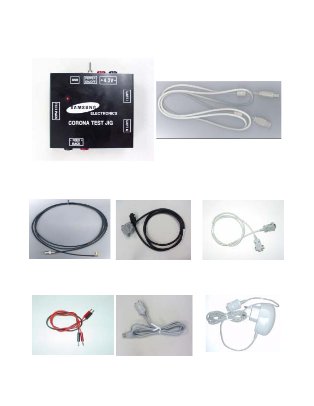
3-3. Test Jig (GH80-03306A)
3-3-2. RF Test Cable
(GH39-00283A)
3-3-3. Test Cable
3-3-1. USB JIG Cable
(GH39-00337A)
3-3-4. Serial Cable
(CSA LL64151-A)
3-3-5. Power Supply Cable
SAMSUNG Proprietary-Contents may change without notice
This Document can not be used without Samsung's authorization
3-3-6. DATA CABLE
(GH39-00331A]
3-4
3-3-7. TA
(GH44-00482A)
4. Electrical Parts List
Design LOC Description SEC CODE
ANT102 ANTENNA-CHIP 4202-001066
C100,C102,C103,C111 C-CERAMIC,CHIP 2203-000812
C101,C108,C112 C-CERAMIC,CHIP 2203-001259
C104,C105,C114 C-CERAMIC,CHIP 2203-002668
C106,C107,C113,C115 C-CERAMIC,CHIP 2203-005288
C116 C-TA,CHIP 2404-001348
C117 C-CERAMIC,CHIP 2203-006190
C118,C119,C131,C133 C-CERAMIC,CHIP 2203-005482
C120,C204,C416 C-CERAMIC,CHIP 2203-000812
C121,C143 C-CERAMIC,CHIP 2203-000654
C122,C126 C-TA,CHIP 2404-001374
C123,C127,C132,C147 C-CERAMIC,CHIP 2203-000628
C124,C128,C135,C201 C-CERAMIC,CHIP 2203-000254
C125,C426 C-CERAMIC,CHIP 2203-000585
C134,C136,C303 C-CERAMIC,CHIP 2203-000438
C137,C140,C413 C-CERAMIC,CHIP 2203-000233
C138 C-CERAMIC,CHIP 2203-000679
C139,C202,C203,C205 C-CERAMIC,CHIP 2203-005482
C141 C-CERAMIC,CHIP 2203-000870
C144 C-CERAMIC,CHIP 2203-006399
C148,C404,C412,C414 C-CERAMIC,CHIP 2203-000628
C200,C306,C402,C403 C-CERAMIC,CHIP 2203-006208
C206,C207,C208,C209 C-CERAMIC,CHIP 2203-005482
C210,C704,C705,C706 C-CERAMIC,CHIP 2203-005682
C211,C212,C213,C214 C-CERAMIC,CHIP 2203-005482
C216,C301,C302,C305 C-CERAMIC,CHIP 2203-005482
C300,C620 C-CERAMIC,CHIP 2203-000254
C304 C-CERAMIC,CHIP 2203-000725
C307,C308,C311,C313 C-CERAMIC,CHIP 2203-005482
C309 C-CERAMIC,CHIP 2203-000550
C315,C317,C318,C320 C-CERAMIC,CHIP 2203-005482
C327,C328,C329 C-CERAMIC,CHIP 2203-005481
C334,C400,C401,C408 C-CERAMIC,CHIP 2203-006562
C405 C-CERAMIC,CHIP 2203-006090
C409,C418,C501,C502 C-CERAMIC,CHIP 2203-006562
C410,C422,C505,C603 C-CERAMIC,CHIP 2203-005482
C411,C420,C421,C429 C-CERAMIC,CHIP 2203-006257
C415,C506,C509 C-TA,CHIP 2404-001268
C423,C427,C428,C717 C-CERAMIC,CHIP 2203-006208
C430 C-CERAMIC,CHIP 2203-006257
C503,C507,C716 C-CERAMIC,CHIP 2203-006093
C510,C614 C-CERAMIC,CHIP 2203-000628
C600,C609 C-TA,CHIP 2404-001402
C601,C604,C607 C-CERAMIC,CHIP 2203-000278
C602,C608 C-CERAMIC,CHIP 2203-000995
C606,C611,C615,C701 C-CERAMIC,CHIP 2203-005482
C616,C617 C-CERAMIC,CHIP 2203-000854
C619 C-CERAMIC,CHIP 2203-006137
C700 C-CERAMIC,CHIP 2203-002443
C702 C-CERAMIC,CHIP 2203-006562
4-1
SAMSUNG Proprietary-Contents may change without notice
This Document can not be used without Samsung's authorization
Electrical Parts List
Design LOC Description SEC CODE
C707,C708,C709,C710 C-CERAMIC,CHIP 2203-005682
C711,C718,C719,C720 C-CERAMIC,CHIP 2203-005682
C712,C713 C-CERAMIC,CHIP 2203-006423
C714,C715 C-CERAMIC,CHIP 2203-005065
C721,C722,C723,C724 C-CERAMIC,CHIP 2203-005682
C725,C726,C727,C728 C-CERAMIC,CHIP 2203-005682
C729 C-CERAMIC,CHIP 2203-005682
CN100 CONNECTOR-COAXIAL 3705-001242
CN500 CONNECTOR-SOCKET 3710-001994
CN501 CONNECTOR-HEADER 3711-005781
CN601 JACK-PHONE 3722-002010
CN700 CONNECTOR-HEADER 3711-005938
CN704 CONNECTOR-HEADER 3711-005818
D500 DIODE-ZENER 0403-001427
F101 FILTER-EMI SMD 2901-001254
L101 INDUCTOR-SMD 2703-002170
L103 INDUCTOR-SMD 2703-002314
L104,L105,L109,L110 INDUCTOR-SMD 2703-002365
L106 INDUCTOR-SMD 2703-002281
L107 INDUCTOR-SMD 2703-002596
L108 INDUCTOR-SMD 2703-002208
L111 INDUCTOR-SMD 2703-001752
L400 CORE-FERRITE BEAD 3301-001120
L401 INDUCTOR-SMD 2703-002840
L402,R103,R113,R118 R-CHIP 2007-000171
L700 CORE-FERRITE BEAD 3301-001534
L701 CORE-FERRITE BEAD 3301-001342
LED700,LED701,LED702 LED 0601-002055
LED703,LED704,LED705 LED 0601-002055
LED706,LED707,LED708 LED 0601-002055
LED709,LED710,LED711 LED 0601-002055
LED712,LED713,LED715 LED 0601-002055
LED717,LED718,LED719 LED 0601-002055
LED720,LED721,LED722 LED 0601-002055
LED723 LED 0601-002055
MODULE1FILTER 2911-000007
OSC100 OSCILLATOR-VCTCXO 2809-001281
OSC400 CRYSTAL-UNIT 2801-004373
Q100,Q101,Q102,Q103 TR-DIGITAL 0504-001151
Q500 TR-DIGITAL 0504-001151
Q700 ;SI1902DL 0505-001469
R100,R101,R102,R104 R-CHIP 2007-000162
R105 R-CHIP 2007-000173
R108,R200,R307,R505 R-CHIP 2007-000148
R110,R117 R-CHIP 2007-000138
R120,R126,R127,R135 R-CHIP 2007-000171
R121,R125 R-CHIP 2007-007014
R122,R124,R128,R131 R-CHIP 2007-000170
R123 R-CHIP 2007-001303
R201,R208,R300,R308 R-CHIP 2007-000171
4-2
SAMSUNG Proprietary-Contents may change without notice
This Document can not be used without Samsung's authorization

Electrical Parts List
Design LOC Description SEC CODE
R203,R204,R600,R603 R-CHIP 2007-000242
R205 R-NETWORK 2011-001394
R206 R-CHIP 2007-000143
R301 R-CHIP 2007-001325
R303,R306,R404,R501 R-CHIP 2007-000162
R309,R318,R403,R407 R-CHIP 2007-000171
R400 R-CHIP 2007-007592
R401,R512 R-CHIP 2007-007334
R402 R-CHIP 2007-007100
R408,R518,R519,R520 R-CHIP 2007-000171
R409,R604,R608 R-CHIP 2007-002796
R500,R502 R-CHIP 2007-000758
R503,R504,R609,R700 R-CHIP 2007-000162
R506 R-CHIP 2007-000152
R507 C-CERAMIC,CHIP 2203-005061
R508,R509 R-CHIP 2007-000170
R510,R611 R-CHIP 2007-007573
R511 R-CHIP 2007-000137
R513 R-CHIP 2007-008275
R514 R-CHIP 2007-007489
R515,R516 R-CHIP 2007-000172
R602,R606,R725 R-CHIP 2007-000148
R605,R607 R-CHIP 2007-000242
R610 R-CHIP 2007-001339
R612 R-CHIP 2007-007480
R701,R702,R703,R704 R-CHIP 2007-002970
R705,R706,R707,R708 R-CHIP 2007-002970
R709,R710,R711,R712 R-CHIP 2007-002970
R713,R714,R727,R729 R-CHIP 2007-002970
R717 R-CHIP 2007-000162
R721,R722 R-CHIP 2007-007317
R730 R-CHIP 2007-000171
R731,R732,R733,R734 R-CHIP 2007-002970
R790,R791 R-CHIP 2007-002970
SIM400 CONNECTOR-CARDEDGE 3709-001384
U100 IC 1205-002709
U101 IC 1201-002223
U103,U303 IC 0801-002237
U200 IC 1205-002647
U300 COMP-SMD GH13-00030A
U301 MEMORY 1108-000022
U302 IC 1204-002138
U304 IC 1209-001618
U306 IC 0801-002882
U400 IC 1203-003767
U401 IC 1203-002837
U402 IC 1203-003787
U404 BATTERY 4302-001177
U405 IC 1203-003568
U500 DIODE-TVS 0406-001188
4-3
SAMSUNG Proprietary-Contents may change without notice
This Document can not be used without Samsung's authorization
Electrical Parts List
Design LOC Description SEC CODE
U501,U700 IC 1203-003737
U502 FILTER-EMI SMD 2901-001315
U503 IC 1203-003742
U600 IC 1001-001333
U603 IC 1202-001068
U701 IC 1009-001010
U702 IC 1203-003046
U703 RF-MODULE 4709-001374
V300,V301,V302,V303 VARISTOR 1405-001082
V400,V701,V702,V703 VARISTOR 1405-001082
V500 THERMISTOR 1404-001221
V704,V705 VARISTOR 1405-001082
ZD500 DIODE-ZENER 0403-001547
ZD600,ZD601 DIODE-TVS 0406-001208
ZD701,ZD702,ZD703 DIODE-TVS 0406-001203
4-4
SAMSUNG Proprietary-Contents may change without notice
This Document can not be used without Samsung's authorization
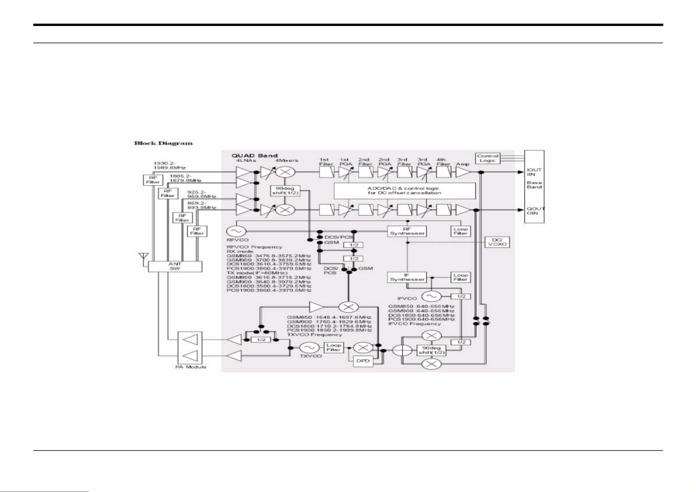
5. Block Diagrams
5-1. RF Solution Block Diagram
5-1
SAMSUNG Proprietary-Contents may change without notice
This Document can not be used without Samsung's authorization
 Loading...