

Samsung SGH-E730 Service Manual
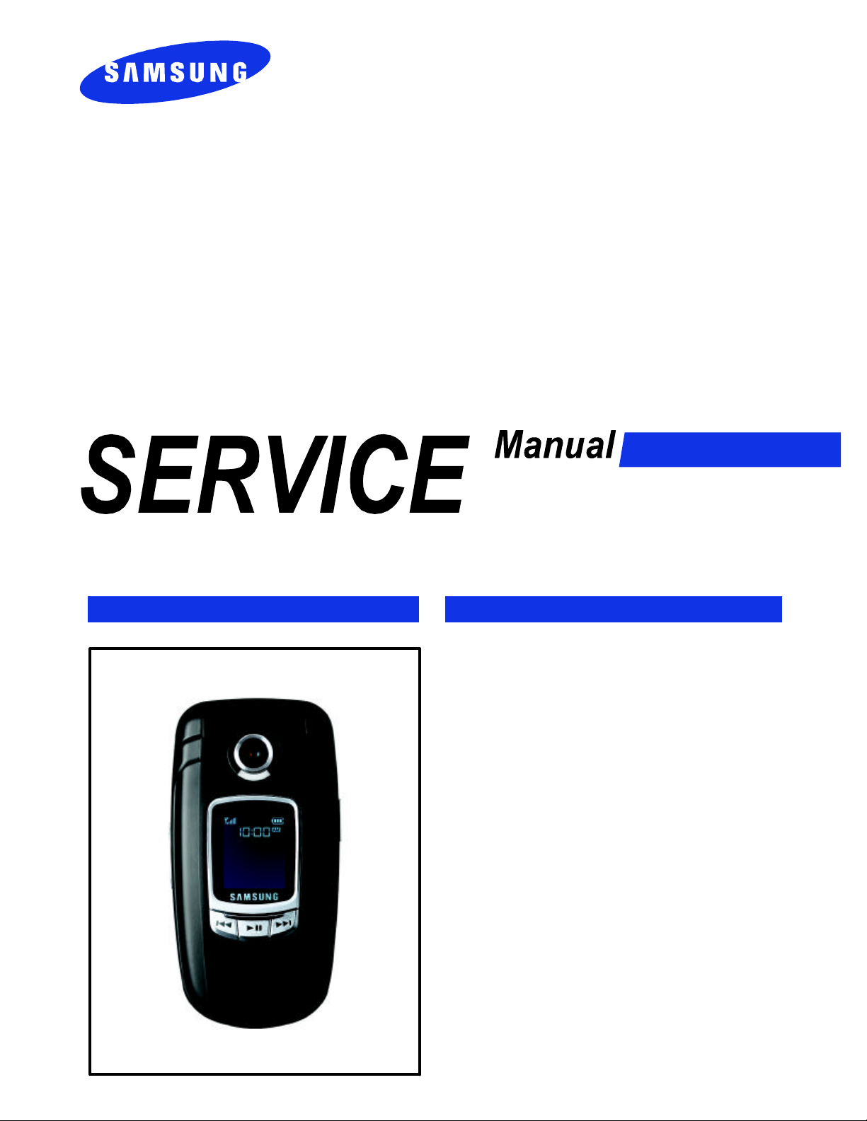
GSM TELEPHONE
SGH-E730
GSM TELEPHONE
CONTENTS
1. Specification
2. Circuit Description
3. Exploded Views and Parts List
4. Electrical Parts List
5. Block Diagrams
6. PCB Diagrams
7. Flow Chart of Troubleshooting
his Service Manual is a property of Samsung Electronics Co.,Ltd.
ny unauthorized use of Manual can be punished under applicable
nternational and/or domestic law.
ⓒ
Samsung Electronics Co.,Ltd. June. 2005
Printed in Korea.
Code No.: GH68-07424A
BASIC.
1. Specification
1-1. GSM General Specification
GSM900
Phase 1
Freq. Band[MHz]
Uplink/Downlink
ARFCN range 1~124
Tx/Rx spacing 45MHz 45MHz 95MHz
Mod. Bit rate
/ Bit Period
Time Slot Period
/ Frame Period
Modulation 0.3GMSK 0.3GMSK 0.3GMSK
MS Power 33dBm~5dBm 33dBm~5dBm 30dBm~0dBm
890~915
935~960
270.833kbps
3.692us
576.9us
4.615ms
EGSM 900
Phase 2
880~915
925~960
0~124 &
975~1023
270.833kbps
3.692us
576.9us
4.615ms
DCS1800
Phase 1
1710~1785
1805~1880
512~885
270.833kbps
3.692us
576.9us
4.615ms
PCS1900
1850~1910
1930~1990
512~810
80MHz
270.833kbps
3.692us
576.9us
4.615ms
0.3GMSK
30dBm~0dBm
Power Class 5pcl ~ 19pcl 5pcl ~ 19pcl 0pcl ~ 15pcl
Sensitivity -102dBm -102dBm -100dBm
TDMA Mux 8 8 8
Cell Radius 35Km 35Km 2Km
0pcl ~ 15pcl
-100dBm
8
-
1-1
SAMSUNG Proprietary-Contents may change without notice
This Document can not be used without Samsung's authorization
Specification
1-2. GSM TX power class
TX Power
control level
5 33±3 dBm
6 31±3 dBm
7 29±3 dBm
8 27±3 dBm
9 25±3 dBm
10 23±3 dBm
11 21±3 dBm
GSM900
TX Power
control level
0 30±3 dBm
1 28±3 dBm
2 26±3 dBm
3 24±3 dBm
4 22±3 dBm
5 20±3 dBm
6 18±3 dBm
DCS1800
TX Power
control level
0 30±3 dBm
1 28±3 dBm
2 26±3 dBm
3 24±3 dBm
4 22±3 dBm
5 20±3 dBm
6 18±3 dBm
PCS1900
12 19±3 dBm
13 17±3 dBm
14 15±3 dBm
15 13±3 dBm
16 11±5 dBm
17 9±5 dBm
18 7±5 dBm
19 5±5 dBm
7 16±3 dBm
8 14±3 dBm
9 12±4 dBm
10 10±4 dBm
11 8±4dBm
12 6±4 dBm
13 4±4 dBm
14 2±5 dBm
7 16±3 dBm
8 14±3 dBm
9 12±4 dBm
10 10±4 dBm
11 8±4dBm
12 6±4 dBm
13 4±4 dBm
14 2±5 dBm
15 0±5 dBm
1-2
15 0±5 dBm
SAMSUNG Proprietary-Contents may change without notice
This Document can not be used without Samsung's authorization
2. Circuit Description
2-1. SGH-E730 RF Circuit Description
2-1-1. RX PART
- ANTENNA SWITCH (Module1 Front End Module)
→
Switching Tx, Rx path for GSM900, DCS1800 and PCS1900 by logic controlling.
- ANTENNA SWITCH Control Losic (Module1)→Truth Table
VC1 VC2 VC3
Tx Mode (GSM900) H L L
Tx Mode (DCS1800/1900) L H L(H)
Rx Mode (GSM900) L L L
Rx Mode (DCS1800) L L L
Rx Mode (PCS1900) L L H
- VC-TCXO (U102)
This module generates the 26MHz reference clock to drive the logic and RF.
It is turned on when the supply voltage Vcc(SYN) is applied.
After buffering a reference clock of 26MHz is supplied to the other parts of the system
through the transceiver pin CLKOUT.
- TRANSCEIVER (U100)
This chip is fully integrated GSM GPRS quad-band transceiver with transmit baluns(balanced-unbalanced matching devices)
, loop filters and most of the passive component in it.
And also fully integrated fractional N RF sy nthesizer with AFC control possibility, RF VCO with integrated supply
regulator. Semi integrated reference oscillator with integrated supply regulator.
RF Receiver front-end amplifies the E-GSM900, DCS1800 and PCS1900 aerial signal, convert the chosen channel
down to a low IF of 100kHz.
In IF section, further amplifies the wanted channel output level to the desired value and rejects DC.
2-1-2. TX PART
The transmitter is fully differential using a direct up conversion architecture. It consists of a signal side band
power up mixer. Gain is controlled by 6 dB via 3-wire serial bus programing. The fully integrated VCO and power
mixer achieve LO suppression, quadrature phase error, quadrature amplitude balance and low noise floor specification.
Output matching/balun components drive a standard 50 ohms single ended load.
2-1
SAMSUNG Proprietary-Contents may change without notice
This Document can not be used without Samsung's authorization

Circuit Description
2-2. Baseband Circuit description of SGH-E730
2-2-1. PCF50603 (U400)
- Power Management
Eight low-dropout regulators designed specifically for GSM applications power the terminal and help ensure optimal
system performance and long battery life. A programmable boost converter provides support for 1.8V, 3.0V SIMs,
while a self-resetting, electronically fused switch supplies power to external accessories. Ancillary support functions,
such as RTC module and High Voltage Charge pump, Clock generator, aid in reducing both board area and system
complexity.
I2C BUS serial interface provides access to control and configuration registers. This interface gives a microprocessor
full control of the PCF50603 and enables system designers to maximize both standby and talk times.
Supervisory functions. including a reset generator, an input voltage monitor, and a temperature sensor, support reliable
system design. These functions work together to ensure proper sy stem behavior during start-up or in the event of a
fault condition(low microprocessor voltage, insufficient battery energy, or excessive die temperature).
- Clock Generator
The Clock Generator (CG) generates all clocks for internal and external usage. The 32.768 kHz crystal oscillator
provides an accurate low clock frequency for the PCF50603 and other circuitry.
2-2-2. LCD Connector
LCD is consisted of main LCD(color 262K TFT LCD) and sub LCD(color 65K OLED LCD)
Chip select signals in the U305, LCD_MAIN_CS, LCD_SUB_CS can enable LCD. BACKLIGHT signal enables white
LED of main LCD. These signal is from U200.
16-bit data lines(LD(0)~LD(15)) transfers data and commands to LCD. Data and commands use "RS" signal. If this signal
is high, Inputs to LCD are commands. If it is low, Inputs to LCD are data. The signal which informs the input or output
state to LCD, is required. But this system is not necessary this signal. So "L_WR" signal is used to write data or
commands to LCD. Power signals for LCD are "VDD_IO_HIGH".
2-2-3. BLUE TOOTH
This system uses Blue Tooth module, UGNZ3, ALPS. This has signals, "BT_INT"(Interrupt signal), "RXD2"(input data)
and "TXD2"(output data), PCM control signal(DCL[PCMCLK], DO[PCM_IN], DU[PCM_OUT], FSC[PCM_SYNC]) These
signals are connected to PCF5212EL1EL1.
2-2-4. Key
This is consisted of key interface pins KEY_ROW(0:4) and KEY_COL(0:4) in PCF5212EL1EL1. These signals compose
the matrix. Result of matrix informs the key status to key interface in the PCF5212EL1EL1. Power on/off key is
seperated from the matrix. So power on/off signal is connected with PCF50603 to enable PCF50603. Key LED is
consisted of 12 white LEDs for main key. Main key LED use the 3.3V LDO for a supply voltage. KEY_LED_ON
signal enables 12 white LED.
"FLIP" informs the status of folder (open or closed) to the PCF5212EL1EL1. This uses the hall effect IC, EM-1681-FT.
A magnet under LCD enables EM-1681-FT.
2-2
SAMSUNG Proprietary-Contents may change without notice
This Document can not be used without Samsung's authorization

Circuit Description
2-2-5. EMI ESD Filter
This system uses the EMI ESD filter, U500 to protect noise from IF CONNECTOR part.
2-2-6. IF connetor
It is 18-pin connector. They are designed to use VBAT, V_EXT_CHARGE, USB_D+, +VBUS, USB_D-, TXD1, RXD1,
AUX_ON, EXT1, EXT2, and GND. They connected to power supply IC, microprocessor and signal processor IC.
2-2-7. Battery Charge Management
A complete constant-current/constant-voltage linear charger for single cell lithium-ion batteries.
If TA connected to phone, "V_EXT_CHARGE" enable charger IC and supply current to battery.
When fault condition caused, "CHG_ON" signal level change low to high and charger IC stop charging process.
2-2-8. Audio
HFR_P and HFR_N from PCF5212EL1EL1 are connected to the main speaker via analog switches. MIC_P and MIC_N
are connected to the main MIC as well. EAR1 is the source of External Speaker. YMU765 is a synthesizer LSI for
mobile phones. This LSI has a built-in speaker amplifier for outputting sounds that are used by mobile phones in addition
to game sounds and ringing melodies that are replayed by a synthesizer.
The synthesizer section adopts“stereophonic hybrid synthesizer system”that are given advantages of both FM
synthesizers and Wave Table sy nthesizers to allow simultaneous generation of up to 32 FM voices and 32 Wave
Table voices.
It provides simultaneous generation of up to 64 tones by stereophonic hybrid synthesizer.
YMU765 has built a speaker amplifier of which maximum out is 580 mW at SPVDD=3.6V in this device.
There is Stereophonic analog output for Headphone.
2-2-9. Memory
This system uses Samsung's memory, KAP17WG00M-D444. The KAP17WG00M-D444 is a Multi Chip Package Memory
which combines 256Mbit Synchronous Burst Multi Bank NOR Flash Memory and two 1Gbit OneNAND Flash and
128Mbit Synchronous Burst UtRAM.
It has 16 bit data line, HD[0~15] which is connected to PCF5212EL1EL1 and MV3315DOQ, also has 24 bit address
lines,
HA[1~24]. There are 3 chip select signals, CS0n_FLASH, CS4n_NAND, and CS1n_RAM.
In the Wrting process, WEn is fallen to low and it enables writing process to operate. During reading process,
OEn is fallen to low and it enables reading process to operate. Each chip select signals in the PCF5212EL1EL1 choose
different memories.
2-2-10. PCF5212EL1EL1
The PCF5212EL1EL1 is mainly composed of embeded DSP and ARM core. The DSP subsystem includes the Saturn
DSP core with embedded RAM and ROM, and a set of peripherals. It has 24kx16 bits PRAM, 104k*16 bits,
32k*16 XYRAM and 63k*16 XYROM in the DSP.
The ARM946E-S consists of an ARM9E-S processor core, 8 kbyte instruction cache and 8 kbyte data cache,
tghtly-coupled ITCM(Instruction Tightly Coupled Memory) and DTCM(Data Tightly Coupled Memory) memories, a
memory protection unit, and an AMBA(Advanced Microcontroller Bus Architecture) AHB(Advanced
High-performance Bus) bus interface with a write buffer.
2-3
SAMSUNG Proprietary-Contents may change without notice
This Document can not be used without Samsung's authorization

Circuit Description
HD(0:15), data lines and HA(0:23), address lines are connected to KBJ10KB00M (memory), MV3315DOQ (image dsp)
and YMU765 (melody IC). It has 64 kbyte SC RAM (0.5 Mbit) and 32 kbyte SC program ROM for bootstrap
loader in the ARM core.
HD(0:15), data lines and HA(0:23), address lines are connected to memory and YMU765 to communicate.
MV3315DOQ(Camera DSP Chip) controls the communication between ARM core and DSP core.
OEn, WEn control the access of memory. KROW, and KCOL recognize the key string input status. The system
communicates with IrDA via IrDA_TXD, IrDA_RXD.
It has J-TAG control pins (TDI/TDO/TCK) for ARM and DSP core. J-SEL signal controls different access to ARM
and DSP core.
ADC(Analog to Digital Convertor) receives the condition of temperature, battery type and battery voltage.
2-2-11. VC-TCXO-214C6-26.0C (26MHz)
This system uses the 26MHz TCXO, VC-TCXO-214C6-26.0C. AFC control signal form PCF5212EL1 controls
frequency from 26MHz x-tal. It generates the clock frequency. This clock is connected to PCF5212EL1, YMU765 and
HD155166BPEB.
2-2-12. Camera DSP (MV3315DOQ)
MV3315DOQ provides rich video functions up to 30-frame display with minimized tasks in the handset main processor
as well as hardware based real-time JPEG compression and decompression. MV3315DOQ directly transmits and
previews the RGB data to the LCD graphic memory by processing the sensor output data according to the
handset's command. It can save the raw RGB data up to VGA resoultion into its image buffer and allows the
host processor to download with scalable sized compressed data.
It utilizes 16 bit data bus for communication with the main processor, including bus interface types.
2-2-13. FM Radio (TEA5761UK)
The TEA5761 is a single chip electronically tuned FM stereo radio for low voltage application with fully integrated IF
selectivity and demodulation.
TEA5761UK provide FM mixer for conversion of the US/Europe (87.5 MHz to 108 MHz) and Japanese FM band (76
MHz to 90 MHz) to IF.Preset tuning to receive Japanese TV audio up to 108 MHz, raster 100 kHz. and is connected to
PCF5212EL1 of I2C.
2-4
SAMSUNG Proprietary-Contents may change without notice
This Document can not be used without Samsung's authorization
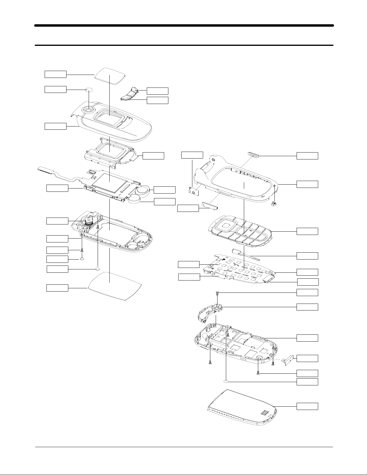
3. Exploded View and Parts List
3-1. Exploded View
QWD02
QCW01
QFU01
QLC01
QCA01
QFL01
QCR05
QSC05
QSC08
QMW01
QKP02
QME03
QLB00
QMI02
QMO01
QRF03
QVO01
QME01
QVK01
QCK01
QFR01
QKP01
QCA02
QMI01
QMP01
QCR12
3-1
SAMSUNG Proprietary-Contents may change without notice
This Document can not be used without Samsung's authorization
QAN02
QRE01
QIF01
QCR06
QRF01
QBA01
Exploded view and Part List
3-2. Parts List
Location NO. SEC CODE Description
QAN02 GH42-00568A INTENNA-SGHE730;HIR-01503-0000AA,SGH
QBA01 GH43-01773A BATTERY-800MAH,B/K,ENG,M;BST3578BE,S
QCA01 GH59-01977A UNIT-CAMERA;SGH-E730,IC03037AA,-,XEF
QCA02 GH59-02072A UNIT-CAMERA KEY;SGH-E730,H/K F.P.C A
QCR05 6001-001478 SCREW-MACHINE;PH,+,M1.4,L3,ZPC(BLK),
QCR06 6001-001155 SCREW-MACHINE;PH(PI2.5),+,M1.4,L3.5,
QCR12 6001-001530 SCREW-MACHINE;PH,+,M1.4,L2.5,ZPC(BLK
QCW01 GH72-19281A PMO-CAMERA LENS;SGH-E730,ACRYL,TRP,P
QFL01 GH75-06733A MEC-FOLDER LOWER;SGH-E730,XET,PC,-,QFR01 GH75-06729A MEC-FRONT COVER;SGH-E730,XET,PC,-,-,
QVO01 GH75-06236A MEC-VOLUME KEY;SGH-E730,EU,PC,17.8X3
QCK01 GH75-06237A MEC-CAMERA KEY;SGH-E730,EU,PC,3.7X12
QFU01 GH75-06732A MEC-FOLDER UPPER;SGH-E730,XET,PC,-,-
QIF01 GH72-19296A PMO-IF COVER;SGH-E730,PC+ELASTOMER,N
QKP01 GH75-06730A MEC-KEYPAD(XET/BLK);SGH-E730,XET,PC,
QKP02 GH75-06731A MEC-KEY FOLD;SGH-E730,XET,PC,-,-,-,S
QLB00 GH75-06737A MEC-LCD BRACKET;SGH-E730,XET,PC,-,-,
QLC01 GH07-00697A LCD-SGHE730 MODEL;UF-17E077-A,SGH-E7
QME01 GH59-02069A UNIT-METAL DOME;SGH-E730,METAL DOME,
QME03 GH59-02071A UNIT-MP3 KEY;SGH-E730,SGH-E730 MP3/K
QMI01 GH30-00188A MICROPHONE-ASSY-SGHE730;2,130~500uA,
QMI02 3001-001750 MICRO SPEAKER;0.7W,8ohm,86dB± 2dB,80
QMO01 GH31-00154D MOTOR DC-SGHZ130;DMJBRK20C,SGH-Z130,
QMP01 GH92-02149A PBA MAIN-SGHE730;SGH-E730,XET,EU,PBA
QMW01 GH75-06238A MEC-MAIN WINDOW;SGH-E730,EU,PC,-,-,-
QRE01 GH75-06734A MEC-REAR COVER;SGH-E730,XET,PC,-,-,-
QRF01 GH74-14614A MPR-SHEET RF;SGH-E730,PC SHEET,PI6.5
QRF03 GH72-19271A PMO-EAR COVER;SGH-E730,PC,BLK,10.6X6
QSC05 GH73-04080A RMO-RUBBER SCREW CAP(L);SGH-E730,SI
QSC08 GH73-04081A RMO-RUBBER SCREW CAP(R);SGH-E730,SI
QVK01 GH59-02070A UNIT-VOLUME KEY;SGH-E730,SGH-E730 V/
QWD02 GH72-19283A PMO-SUB LCD WINDOW;SGH-E730,ACRYL,BL
3-2
SAMSUNG Proprietary-Contents may change without notice
This Document can not be used without Samsung's authorization

SEC CODE Description
6902-000634 BAG PE;LDPE,T0.05,W80,L180,TRP,-,GH44-00954A ADAPTOR-SGHD500 BLK;TAD137EBE,SGH-D5
GH59-02166A UNIT-EARPHONE;SGH-C230,EM-SS550E-STB
GH68-02026A LABEL(P)-WATER SOAK;SCH-X110,NORGE,1
GH68-06835A LABEL(R)-MAIN(EU);SGH-E730,EU,POLYES
GH68-06897A MANUAL-USE;SGH-E730,XEF,FRENCH,FRAN,
GH68-07013A MANUAL-WEEE CARD;SGH-E720,SEC,ENGLIS
GH69-02842J BOX(P)-SGHE730(IKF_EU);SGH-E730,SC30
GH69-02845A CUSHION-CASE(1-2);SGH-E730,PULP,T0.8
GH74-05962A MPR-FRONT FILTER;SGH-E700,BUZICPO,16
GH74-05963A MPR-BOHO FOLDER LOWER;SGH-E700,3M 41
GH74-14607A MPR-BOHO VINYL F/UPPER;SGH-E730,3M 4
GH74-14608A MPR-BOHO VINYL F/LOWER;SGH-E730,3M 4
GH74-14609A MPR-BOHO VINYL REAR;SGH-E730,3M 4187
Exploded view and Part List
GH74-15238A MPR-SPONGE MOTOR;SGH-E730,PORON,PI10
GH74-15350A MPR-BOHO VINYL LCD CONN;SGH-E730,#95
GH74-15507A MPR-TAPE PCB ESD 1;SGH-E730,CONDUCTI
GH74-15508A MPR-TAPE PCB ESD 2;SGH-E730,CONDUCTI
GH74-15509A MPR-TAPE PCB INSUALTION;SGH-E730,3M
GH74-15513A MPR-SPONGE PCB ESD;SGH-E730,CONDUCTI
GH74-15582A MPR-BOHO VINYL SUB WIN;SGH-E730,PVC,
GH74-15635A MPR-TAPE LCD ESD 1;SGH-E730,3M EAD16
GH74-15641A MPR-TAPE LCD ESD 3;SGH-E730,3M 1352B
GH75-03207E MEC-HAND STRAP;SGH-C100,SEC,-,-,BLK(
3-3
SAMSUNG Proprietary-Contents may change without notice
This Document can not be used without Samsung's authorization
Exploded view and Part List
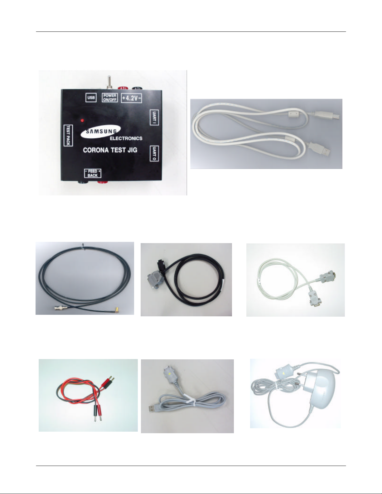
3-3. Test Jig (GH80-03306A)
3-3-2. RF Test Cable
(GH39-00283A)
3-3-3. Test Cable
3-3-1. USB JIG Cable
(GH39-00337A)
3-3-4. Serial Cable
(CSA LL64151-A)
3-3-5. Power Supply Cable
SAMSUNG Proprietary-Contents may change without notice
This Document can not be used without Samsung's authorization
3-3-6. DATA CABLE
(GH39-00331A]
3-4
3-3-7. TA
(GH44-00482A)
4. Electrical Parts List
SEC CODE Design LOC Description
0403-001387 ZD500 DIODE-ZENER
0403-001427 ZD501 DIODE-ZENER
0406-001104 ZD601 DIODE-TVS
0406-001188 U500 DIODE-TVS
0406-001190 ZD600 DIODE-TVS
0406-001190 ZD700 DIODE-TVS
0406-001201 V700 DIODE-TVS
0406-001203 V401 DIODE-TVS
0406-001208 ZD701 DIODE-TVS
0504-001151 Q200 TR-DIGITAL
0504-001151 Q201 TR-DIGITAL
0504-001151 Q202 TR-DIGITAL
0504-001151 Q203 TR-DIGITAL
0504-001151 Q500 TR-DIGITAL
0505-001332 Q300 FET-SILICON
0601-001819 LED700 LED
0601-001819 LED701 LED
0601-001819 LED702 LED
0601-001819 LED703 LED
0601-001819 LED704 LED
0601-001819 LED705 LED
0601-001819 LED706 LED
0601-001819 LED707 LED
0601-001819 LED708 LED
0601-001819 LED709 LED
0601-001819 LED710 LED
0601-001819 LED711 LED
0801-003022 U304 IC-CMOS LOGIC
0801-003025 U302 IC-CMOS LOGIC
1001-001221 U600 IC-ANALOG SWITCH
1001-001231 U604 IC-ANALOG MULTIPLEX
1001-001231 U701 IC-ANALOG MULTIPLEX
1001-001306 U602 IC-ANALOG MULTIPLEX
1009-001020 U503 IC-HALL EFFECT S/W
1108-000022 U303 IC-MCP
1201-002223 U101 IC-TRANSMITTER
1202-001068 U601 IC-VOLTAGE AMP
1203-003568 U400 IC-POWER SUPERVISOR
1203-003736 U402 IC DC/DC CONVERTER
1203-003737 U401 IC-POSI. FIXED REG
1203-003737 U700 IC-POSI. FIXED REG
1203-003742 U502 IC-BATTERY
1204-002138 U300 IC-AUDIO AMP
1204-002398 U603 IC-TUNNER
1205-002647 U200 IC-COMM. CONTROLLER
1205-002709 U100 IC-MODEM
1404-001221 V500 THERMISTOR
1405-001082 V400 VARISTOR
1405-001082 V702 VARISTOR
1405-001082 V703 VARISTOR
4-1
SAMSUNG Proprietary-Contents may change without notice
This Document can not be used without Samsung's authorization
Electrical Parts List
SEC CODE Design LOC Description
1405-001082 V704 VARISTOR
1405-001128 V705 VARISTOR
1405-001128 V706 VARISTOR
2007-000137 R511 R-CHIP
2007-000138 R105 R-CHIP
2007-000138 R116 R-CHIP
2007-000138 R616 R-CHIP
2007-000140 R625 R-CHIP
2007-000141 R310 R-CHIP
2007-000141 R311 R-CHIP
2007-000143 R218 R-CHIP
2007-000148 R201 R-CHIP
2007-000148 R305 R-CHIP
2007-000148 R308 R-CHIP
2007-000148 R504 R-CHIP
2007-000148 R602 R-CHIP
2007-000151 R306 R-CHIP
2007-000152 R506 R-CHIP
2007-000162 R202 R-CHIP
2007-000162 R204 R-CHIP
2007-000162 R207 R-CHIP
2007-000162 R212 R-CHIP
2007-000162 R216 R-CHIP
2007-000162 R307 R-CHIP
2007-000162 R309 R-CHIP
2007-000162 R317 R-CHIP
2007-000162 R319 R-CHIP
2007-000162 R405 R-CHIP
2007-000162 R500 R-CHIP
2007-000162 R503 R-CHIP
2007-000162 R505 R-CHIP
2007-000162 R513 R-CHIP
2007-000162 R606 R-CHIP
2007-000162 R611 R-CHIP
2007-000162 R621 R-CHIP
2007-000162 R716 R-CHIP
2007-000170 R208 R-CHIP
2007-000170 R209 R-CHIP
2007-000170 R210 R-CHIP
2007-000170 R211 R-CHIP
2007-000170 R508 R-CHIP
2007-000170 R509 R-CHIP
2007-000171 R100 R-CHIP
2007-000171 R108 R-CHIP
2007-000171 R109 R-CHIP
2007-000171 R110 R-CHIP
2007-000171 R111 R-CHIP
2007-000171 R113 R-CHIP
2007-000171 R114 R-CHIP
2007-000171 R115 R-CHIP
4-2
SAMSUNG Proprietary-Contents may change without notice
This Document can not be used without Samsung's authorization

SEC CODE Design LOC Description
2007-000171 R117 R-CHIP
2007-000171 R118 R-CHIP
2007-000171 R119 R-CHIP
2007-000171 R121 R-CHIP
2007-000171 R122 R-CHIP
2007-000171 R200 R-CHIP
2007-000171 R203 R-CHIP
2007-000171 R205 R-CHIP
2007-000171 R206 R-CHIP
2007-000171 R220 R-CHIP
2007-000171 R301 R-CHIP
2007-000171 R302 R-CHIP
2007-000171 R304 R-CHIP
2007-000171 R316 R-CHIP
2007-000171 R318 R-CHIP
2007-000171 R403 R-CHIP
2007-000171 R404 R-CHIP
2007-000171 R610 R-CHIP
2007-000171 R613 R-CHIP
2007-000171 R619 R-CHIP
2007-000171 R620 R-CHIP
2007-000171 R622 R-CHIP
2007-000171 R623 R-CHIP
2007-000171 R624 R-CHIP
2007-000171 R712 R-CHIP
2007-000171 R713 R-CHIP
2007-000171 R714 R-CHIP
2007-000171 R715 R-CHIP
2007-000173 R101 R-CHIP
2007-000242 R601 R-CHIP
2007-000242 R603 R-CHIP
2007-000758 R501 R-CHIP
2007-000758 R502 R-CHIP
2007-000775 R617 R-CHIP
2007-000831 R605 R-CHIP
2007-001303 R314 R-CHIP
2007-001325 R300 R-CHIP
2007-001325 R618 R-CHIP
2007-001339 R612 R-CHIP
2007-002796 R406 R-CHIP
2007-002796 R604 R-CHIP
2007-002970 R700 R-CHIP
2007-002970 R701 R-CHIP
2007-002970 R702 R-CHIP
2007-002970 R703 R-CHIP
2007-002970 R704 R-CHIP
2007-002970 R705 R-CHIP
2007-002970 R705 R-CHIP
2007-002970 R706 R-CHIP
2007-002970 R707 R-CHIP
4-3
Electrical Parts List
SAMSUNG Proprietary-Contents may change without notice
This Document can not be used without Samsung's authorization

Electrical Parts List
SEC CODE Design LOC Description
2007-002970 R708 R-CHIP
2007-002970 R709 R-CHIP
2007-002970 R710 R-CHIP
2007-002970 R711 R-CHIP
2007-007014 R313 R-CHIP
2007-007014 R315 R-CHIP
2007-007100 R402 R-CHIP
2007-007101 R303 R-CHIP
2007-007107 R401 R-CHIP
2007-007137 R214 R-CHIP
2007-007137 R215 R-CHIP
2007-007308 R514 R-CHIP
2007-007334 R512 R-CHIP
2007-007480 R608 R-CHIP
2007-007489 R515 R-CHIP
2007-007573 R510 R-CHIP
2007-007573 R607 R-CHIP
2007-008812 R400 R-CHIP
2011-001394 R217 R-CHIP
2203-000233 C136 C-CERAMIC,CHIP
2203-000233 C312 C-CERAMIC,CHIP
2203-000233 C409 C-CERAMIC,CHIP
2203-000233 C620 C-CERAMIC,CHIP
2203-000254 C126 C-CERAMIC,CHIP
2203-000254 C129 C-CERAMIC,CHIP
2203-000254 C131 C-CERAMIC,CHIP
2203-000254 C138 C-CERAMIC,CHIP
2203-000254 C202 C-CERAMIC,CHIP
2203-000254 C310 C-CERAMIC,CHIP
2203-000254 C610 C-CERAMIC,CHIP
2203-000254 C619 C-CERAMIC,CHIP
2203-000278 C112 C-CERAMIC,CHIP
2203-000278 C113 C-CERAMIC,CHIP
2203-000278 C114 C-CERAMIC,CHIP
2203-000278 C601 C-CERAMIC,CHIP
2203-000278 C607 C-CERAMIC,CHIP
2203-000278 C612 C-CERAMIC,CHIP
2203-000359 C400 C-CERAMIC,CHIP
2203-000438 C135 C-CERAMIC,CHIP
2203-000438 C137 C-CERAMIC,CHIP
2203-000438 C139 C-CERAMIC,CHIP
2203-000438 C303 C-CERAMIC,CHIP
2203-000628 C125 C-CERAMIC,CHIP
2203-000628 C128 C-CERAMIC,CHIP
2203-000628 C130 C-CERAMIC,CHIP
2203-000628 C132 C-CERAMIC,CHIP
2203-000654 C315 C-CERAMIC,CHIP
2203-000679 C300 C-CERAMIC,CHIP
2203-000679 C313 C-CERAMIC,CHIP
2203-000679 C624 C-CERAMIC,CHIP
4-4
SAMSUNG Proprietary-Contents may change without notice
This Document can not be used without Samsung's authorization

SEC CODE Design LOC Description
2203-000679 C405 C-CERAMIC,CHIP
2203-000679 C407 C-CERAMIC,CHIP
2203-000696 C604 C-CERAMIC,CHIP
2203-000812 C100 C-CERAMIC,CHIP
2203-000812 C101 C-CERAMIC,CHIP
2203-000812 C103 C-CERAMIC,CHIP
2203-000812 C120 C-CERAMIC,CHIP
2203-000812 C205 C-CERAMIC,CHIP
2203-000812 C213 C-CERAMIC,CHIP
2203-000812 C215 C-CERAMIC,CHIP
2203-000812 C218 C-CERAMIC,CHIP
2203-000812 C221 C-CERAMIC,CHIP
2203-000812 C224 C-CERAMIC,CHIP
2203-000812 C411 C-CERAMIC,CHIP
2203-000812 C706 C-CERAMIC,CHIP
2203-000812 C707 C-CERAMIC,CHIP
2203-000812 C708 C-CERAMIC,CHIP
2203-000812 C716 C-CERAMIC,CHIP
2203-000995 C605 C-CERAMIC,CHIP
2203-000995 C611 C-CERAMIC,CHIP
2203-000995 C623 C-CERAMIC,CHIP
2203-001153 C421 C-CERAMIC,CHIP
2203-001259 C106 C-CERAMIC,CHIP
2203-001259 C108 C-CERAMIC,CHIP
2203-001259 C709 C-CERAMIC,CHIP
2203-001259 C710 C-CERAMIC,CHIP
2203-001259 C711 C-CERAMIC,CHIP
2203-001259 C712 C-CERAMIC,CHIP
2203-001259 C713 C-CERAMIC,CHIP
2203-001259 C714 C-CERAMIC,CHIP
2203-001259 C715 C-CERAMIC,CHIP
2203-002443 C500 C-CERAMIC,CHIP
2203-002525 C306 C-CERAMIC,CHIP
2203-002668 C104 C-CERAMIC,CHIP
2203-002668 C115 C-CERAMIC,CHIP
2203-003054 C615 C-CERAMIC,CHIP
2203-003054 C617 C-CERAMIC,CHIP
2203-005050 C117 C-CERAMIC,CHIP
2203-005288 C105 C-CERAMIC,CHIP
2203-005288 C116 C-CERAMIC,CHIP
2203-005480 C311 C-CERAMIC,CHIP
2203-005480 C618 C-CERAMIC,CHIP
2203-005480 C621 C-CERAMIC,CHIP
2203-005480 C622 C-CERAMIC,CHIP
2203-005480 C627 C-CERAMIC,CHIP
2203-005482 C133 C-CERAMIC,CHIP
2203-005482 C134 C-CERAMIC,CHIP
2203-005482 C201 C-CERAMIC,CHIP
2203-005482 C203 C-CERAMIC,CHIP
2203-005482 C204 C-CERAMIC,CHIP
4-5
Electrical Parts List
SAMSUNG Proprietary-Contents may change without notice
This Document can not be used without Samsung's authorization

Electrical Parts List
SEC CODE Design LOC Description
2203-005482 C206 C-CERAMIC,CHIP
2203-005482 C207 C-CERAMIC,CHIP
2203-005482 C208 C-CERAMIC,CHIP
2203-005482 C209 C-CERAMIC,CHIP
2203-005482 C210 C-CERAMIC,CHIP
2203-005482 C211 C-CERAMIC,CHIP
2203-005482 C212 C-CERAMIC,CHIP
2203-005482 C214 C-CERAMIC,CHIP
2203-005482 C217 C-CERAMIC,CHIP
2203-005482 C301 C-CERAMIC,CHIP
2203-005482 C302 C-CERAMIC,CHIP
2203-005482 C305 C-CERAMIC,CHIP
2203-005482 C307 C-CERAMIC,CHIP
2203-005482 C308 C-CERAMIC,CHIP
2203-005482 C309 C-CERAMIC,CHIP
2203-005482 C314 C-CERAMIC,CHIP
2203-005482 C318 C-CERAMIC,CHIP
2203-005482 C319 C-CERAMIC,CHIP
2203-005482 C406 C-CERAMIC,CHIP
2203-005482 C419 C-CERAMIC,CHIP
2203-005482 C502 C-CERAMIC,CHIP
2203-005482 C503 C-CERAMIC,CHIP
2203-005482 C505 C-CERAMIC,CHIP
2203-005482 C603 C-CERAMIC,CHIP
2203-005482 C606 C-CERAMIC,CHIP
2203-005482 C626 C-CERAMIC,CHIP
2203-006053 C304 C-CERAMIC,CHIP
2203-006093 C413 C-CERAMIC,CHIP
2203-006093 C501 C-CERAMIC,CHIP
2203-006137 C616 C-CERAMIC,CHIP
2203-006190 C222 C-CERAMIC,CHIP
2203-006190 C223 C-CERAMIC,CHIP
2203-006208 C401 C-CERAMIC,CHIP
2203-006208 C412 C-CERAMIC,CHIP
2203-006208 C414 C-CERAMIC,CHIP
2203-006208 C418 C-CERAMIC,CHIP
2203-006208 C422 C-CERAMIC,CHIP
2203-006208 C423 C-CERAMIC,CHIP
2203-006257 C408 C-CERAMIC,CHIP
2203-006257 C415 C-CERAMIC,CHIP
2203-006257 C416 C-CERAMIC,CHIP
2203-006257 C424 C-CERAMIC,CHIP
2203-006257 C425 C-CERAMIC,CHIP
2203-006257 C628 C-CERAMIC,CHIP
2203-006260 C122 C-CERAMIC,CHIP
2203-006324 C404 C-CERAMIC,CHIP
2203-006562 C200 C-CERAMIC,CHIP
2203-006562 C317 C-CERAMIC,CHIP
2203-006562 C402 C-CERAMIC,CHIP
2203-006562 C403 C-CERAMIC,CHIP
4-6
SAMSUNG Proprietary-Contents may change without notice
This Document can not be used without Samsung's authorization
SEC CODE Design LOC Description
2203-006562 C506 C-CERAMIC,CHIP
2203-006562 C625 C-CERAMIC,CHIP
2203-006562 C700 C-CERAMIC,CHIP
2404-001348 C121 C-TA,CHIP
2404-001374 C124 C-TA,CHIP
2404-001374 C127 C-TA,CHIP
2404-001394 C410 C-TA,CHIP
2404-001394 C504 C-TA,CHIP
2404-001402 C600 C-TA,CHIP
2703-001231 L603 INDUCTOR-SMD
2703-001673 L604 INDUCTOR-SMD
2703-001752 L300 INDUCTOR-SMD
2703-002170 L110 INDUCTOR-SMD
2703-002206 L605 INDUCTOR-SMD
2703-002281 L112 INDUCTOR-SMD
2703-002314 L103 INDUCTOR-SMD
2703-002365 L104 INDUCTOR-SMD
2703-002365 L105 INDUCTOR-SMD
2703-002365 L108 INDUCTOR-SMD
2703-002365 L109 INDUCTOR-SMD
2703-002586 L101 INDUCTOR-SMD
2703-002596 L107 INDUCTOR-SMD
2703-002774 L401 INDUCTOR-SMD
2801-004373 OSC400 CRYSTAL-UNIT
2809-001293 U102 OSCILLATOR-VCTCXO
2901-001254 F100 FILTER-EMI SMD
2901-001286 F700 FILTER-EMI SMD
2901-001286 F701 FILTER-EMI SMD
2901-001286 F702 FILTER-EMI SMD
2901-001286 F703 FILTER-EMI SMD
2901-001286 F704 FILTER-EMI SMD
2901-001315 U501 FILTER-EMI SMD
2911-000007 MODULE1 FILTER
3301-001120 L400 CORE-FERRITE BEAD
3301-001438 L600 CORE-FERRITE BEAD
3301-001438 L601 CORE-FERRITE BEAD
3301-001534 L500 CORE-FERRITE BEAD
3301-001789 L200 CORE-FERRITE BEAD
3301-001789 R614 CORE-FERRITE BEAD
3705-001358 CN100 CONNECTOR-COAXIAL
3709-001229 SIM400 CONNECTOR-CARD EDGE
3710-001994 IFC500 CONNECTOR-SOCKET
3711-005880 BTC500 CONNECTOR-HEADER
3711-005918 CN700 CONNECTOR-HEADER
3722-002082 CN600 JACK-PHONE
4302-001180 C426 BATTERY
4709-001371 U301 RF-MODULE
GH13-00030A U305 COMP-SMD
4202-001052 ANT300 C-CERAMIC,CHIP
Electrical Parts List
4-7
SAMSUNG Proprietary-Contents may change without notice
This Document can not be used without Samsung's authorization
 Loading...