

Samsung SGH-E360 Service Manual

GSM TELEPHONE
SGH-E360
GSM TELEPHONE
CONTENTS
1. Specification
2. Circuit Description
3. Exploded Views and Parts List
4. Electrical Parts List
5. Block Diagrams
6. PCB Diagrams
7. Flow Chart of Troubleshooting
This Service Manual is a property of Samsung Electronics Co.,Ltd.
Any unauthorized use of Manual can be punished under applicable
International and/or domestic law.
ⓒ
Samsung Electronics Co.,Ltd. December. 2005
Printed in Korea.
Code No.: GH68-08968A
BASIC.

1. Specification
1-1. GSM General Specification
GSM900
Phase 1
Freq. Band[MHz]
Uplink/Downlink
ARFCN range 1~124
Tx/Rx spacing 45MHz 45MHz 95MHz
Mod. Bit rate
/BitPeriod
Time Slot Period
/ Frame Period
Modulation 0.3GMSK 0.3GMSK 0.3GMSK
MS Power 33dBm~5dBm 33dBm~5dBm 30dBm~0dBm
890~915
935~960
270.833kbps
3.692us
576.9us
4.615ms
EGSM 900
Phase 2
880~915
925~960
0~124 &
975~1023
270.833kbps
3.692us
576.9us
4.615ms
DCS1800
Phase 1
1710~1785
1805~1880
512~885
270.833kbps
3.692us
576.9us
4.615ms
PCS1900
1850~1910
1930~1990
512~810
80MHz
270.833kbps
3.692us
576.9us
4.615ms
0.3GMSK
30dBm~0dBm
Power Class 5pcl ~ 19pcl 5pcl ~ 19pcl 0pcl ~ 15pcl
Sensitivity -102dBm -102dBm -100dBm
TDMA Mux 8 8 8
Cell Radius 35Km 35Km 2Km
0pcl ~ 15pcl
-100dBm
8
-
1-1
SAMSUNG Proprietary-Contents may change without notice
This Document can not be used without Samsung's authorization

Specification
1-2. GSM TX power class
TX Power
control level
5 33±2 dBm
6 31±3 dBm
7 29±3 dBm
8 27±3 dBm
9 25±3 dBm
10 23±3 dBm
11 21±3 dBm
GSM900
TX Power
control level
0 30±2 dBm
1 28±3 dBm
2 26±3 dBm
3 24±3 dBm
4 22±3 dBm
5 20±3 dBm
6 18±3 dBm
DCS1800
TX Power
control level
0 30±2 dBm
1 28±3 dBm
2 26±3 dBm
3 24±3 dBm
4 22±3 dBm
5 20±3 dBm
6 18±3 dBm
PCS1900
12 19±3 dBm
13 17±3 dBm
14 15±3 dBm
15 13±3 dBm
16 11±5 dBm
17 9±5 dBm
18 7±5 dBm
19 5±5 dBm
7 16±3 dBm
8 14±3 dBm
9 12±4 dBm
10 10±4 dBm
11 8±4dBm
12 6±4 dBm
13 4±4 dBm
14 2±5 dBm
7 16±3 dBm
8 14±3 dBm
9 12±4 dBm
10 10±4 dBm
11 8±4dBm
12 6±4 dBm
13 4±4 dBm
14 2±5 dBm
15 0±5 dBm
1-2
15 0±5 dBm
SAMSUNG Proprietary-Contents may change without notice
This Document can not be used without Samsung's authorization

1-3. GSM EDGE TX power class
Specification
TX Power
control level
8 27±3 dBm
9 25±3 dBm
10 23±3 dBm
11 21±3 dBm
12 19±3 dBm
13 17±3 dBm
14 15±3 dBm
GSM900
TX Power
control level
2 26 -4/+3 dBm
3 24±3 dBm
4 22±3 dBm
5 20±3 dBm
6 18±3 dBm
7 16±3 dBm
8 12±3 dBm
DCS1800
TX Power
control level
2 26 -4/+3 dBm
3 24±3 dBm
4 22±3 dBm
5 20±3 dBm
6 18±3 dBm
7 16±3 dBm
8 12±3 dBm
PCS1900
15 13±3 dBm
16 11±5 dBm
17 9±5 dBm
18 7±5 dBm
19 5±5 dBm
9 10±3 dBm
10 14±3 dBm
11 12±4 dBm
12 10±4 dBm
13 8±4dBm
14 6±4 dBm
15 4±4 dBm
9 10±3 dBm
10 14±3 dBm
11 12±4 dBm
12 10±4 dBm
13 8±4dBm
14 6±4 dBm
15 4±4 dBm
1-3
SAMSUNG Proprietary-Contents may change without notice
This Document can not be used without Samsung's authorization

Specification
1-4
SAMSUNG Proprietary-Contents may change without notice
This Document can not be used without Samsung's authorization

2. Circuit Description
2-1. SGH-E360 RF Circuit Description
2-1-1. RX PART
- ANTENNA SWITCH (Module1 Front End Module)
→
Switching Tx, Rx path for GSM900, DCS1800 and PCS1900 by logic controlling.
- ANTENNA SWITCH Control Losic (Module1)→Truth Table
VC1 VC2 VC3
Tx Mode (GSM900) H L L
Tx Mode (DCS1800/1900) L H L(H)
Rx Mode (GSM900) L L L
Rx Mode (DCS1800) L L L
Rx Mode (PCS1900) L L H
- TRANSCEIVER (U102)
This chip is fully integrated GSM GPRS tri-band transceiver with transmit baluns(balanced-unbalanced matching devices) ,
loop filters and most of the passive component in it.
And also fully integrated fractional N RF synthesizer with AFC control possibility, RF VCO with integrated supply
regulator. Semi integrated reference oscillator with integrated supply regulator.
RF Receiver front-end amplifies the E-GSM900, DCS1800 and PCS1900 aerial signal, convert the chosen channel
down to a low IF of 100kHz.
In IF section, further amplifies the wanted channel output level to the desired value and rejects DC.
-PAM(PAM101)
The module consists of two separated line-ups, one for low band(LB 850/900) and one for high band(HB,1800/1900) with
input and output matching and internal power detection function and power control loop in GSM mode.
in GSM mode, the internal power control circuit ensures a stable power output, set by the level of V
compensate variations of supply voltage, input power and temperature, with a control range fully compaliant with ETSI
tome mask and power spectrum requirements
in EDGE mode the output power is controlled by the input power. The V
controlling the quiescent current of the final RF-statges of both line-ups.
signal is used to control the efficiency by
REF
stabilsed to
DAC
2-1-2. TX PART
The transmitter is fully differential using a direct up conversion architecture. It consists of a signal side band
power up mixer. Gain is controlled by 6 dB via 3-wire serial bus programing. The fully integrated VCO and power
mixer achieve LO suppression, quadrature phase error, quadrature amplitude balance and low noise floor specification.
Output matching/balun components drive a standard 50 ohms single ended load.
2-1
SAMSUNG Proprietary-Contents may change without notice
This Document can not be used without Samsung's authorization

Circuit Description
2-2. Baseband Circuit description of SGH-E360
2-2-1. PCF50603 (U400)
- Power Management
Eight low-dropout regulators designed specifically for GSM applications power the terminal and help ensure optimal
system performance and long battery life. A programmable boost converter provides support for 1.8V, 3.0V SIMs,
while a self-resetting, electronically fused switch supplies power to external accessories. Ancillary support functions,
such as RTC module and High Voltage Charge pump, Clock generator, aid in reducing both board area and system
complexity.
I2C BUS serial interface provides access to control and configuration registers. This interface gives a microprocessor
full control of the PCF50603 and enables system designers to maximize both standby and talk times.
Supervisory functions. including a reset generator, an input voltage monitor, and a temperature sensor, support reliable
system design. These functions work together to ensure proper system behavior during start-up or in the event of a
fault condition(low microprocessor voltage, insufficient battery energy, or excessive die temperature).
- Backlight Brightness Modulator
The Backlight Brightness Modulator (BBM) contains a programmable Pulse-width modulator (PWM) and FET to
modulate the intensity of a series of LED’ s or to control a DC/DC converter that drives LCD backlight.
This phone (SGH-E360) use PWM control to contrast the backlight brightness.
- Clock Generator
The Clock Generator (CG) generates all clocks for internal and external usage. The 32.768 kHz crystal oscillator
provides an accurate low clock frequency for the PCF50603 and other circuitry.
2-2-2. LCD Connector
LCD is consisted of main LCD(color 65K TFT LCD) and sub LCD(color 65K OLED LCD)
Chip select signals in the U305, LCD_MAIN_CS, LCD_SUB_CS can enable LCD. BACKLIGHT signal enables white
LED of main LCD. These signal is from U200.
16-bit data lines(LD(0)~LD(15)) transfers data and commands to LCD. Data and commands use "RS" signal. If this signal
is high, Inputs to LCD are commands. If it is low, Inputs to LCD are data. The signal which informs the input or output
state to LCD, is required. But this system is not necessary this signal. So "L_WR" signal is used to write data or
commands to LCD. Power signals for LCD are "VDD_IO_HIGH".
2-2-3. BLUE TOOTH
This system uses Blue Tooth module, LBMA46LCB2, Murata. This has signals, "BT_INT"(Interrupt signal), "RXD2"(input
data) and "TXD2"(output data), PCM control signal(DCL[PCMCLK], DO[PCM_IN], DU[PCM_OUT], FSC[PCM_SYNC])
These signals are connected to PCF5213EL1EL1.
2-2
SAMSUNG Proprietary-Contents may change without notice
This Document can not be used without Samsung's authorization

Circuit Description
2-2-4. Key
This is consisted of key interface pins KEY_ROW(0:4) and KEY_COL(0:4) in PCF5213EL1. These signals compose the
matrix. Result of matrix informs the key status to key interface in the PCF5213EL1. Power on/off key is seperated from
the matrix. So power on/off signal is connected with PCF50603 to enable PCF50603. Key LED is consisted of 12 LEDs.
key LED use the 3.3V LDO(U606) for a supply voltage. KEY_LED_ON signal enables eight white LED.
"FLIP" informs the status of slide (up or down) to the PCF5213EL1. This uses the hall effect IC, EM-1681-FT(U701).
A magnet under LCD enables EM-1681-FT.
2-2-5. EMI ESD Filter
This system uses the EMI ESD filter, U500 to protect noise from IF CONNECTOR part.
2-2-6. IF connetor(IFC500)
It is 18-pin connector. They are designed to use VBAT, V_EXT_CHARGE, USB_D+, +VBUS, USB_D-, TXD1, RXD1,
AUX_ON, EXT1, EXT2 and GND. They connected to power supply IC, microprocessor and signal processor IC.
2-2-7. Battery Charge Management
A complete constant-current/constant-voltage linear charger for single cell lithium-ion batteries.
If TA connected to phone, "V_EXT_CHARGE" enable charger IC and supply current to battery.
When fault condition caused, "CHG_ON" signal level change low to high and charger IC stop charging process.
2-2-8. Audio
HFR_P and HFR_N from PCF5213EL1 are connected to the main speaker via analog switches. MIC_P and MIC_N
are connected to the main MIC as well. EAR1 is the source of External Speaker. YMU762 is a synthesizer LSI for
mobile phones. This LSI has a built-in speaker amplifier for outputting sounds that are used by mobile phones in addition
to game sounds and ringing melodies that are replayed by a synthesizer.
The synthesizer section adopts“stereophonic hybrid synthesizer system”that are given advantages of both FM
synthesizers and Wave Table synthesizers to allow simultaneous generation of up to 32 FM voices and 32 Wave
Table voices. It provides simultaneous generation of up to 40 tones by stereophonic hybrid synthesizer.
YMU762 has built a speaker amplifier of which maximum out is 580 mW at SPVDD=3.6V in this device.
There is Stereophonic analog output for Headphone.
2-2-9. Memory(UME301)
This system uses Samsung's memory, KAP17SG00A. The KAP17SG00A is a Multi Chip Package Memory which
combines 256Mbit Synchronous Burst Multi Bank NOR Flash Memory and two 512Mbit OneNAND Flash and
128Mbit Synchronous Burst UtRAM.
It has 16 bit data line, HD[1~16] which is connected to PCF5213EL1 and MV3018SAQ, also has 24 bit address lines,
HA[1~24]. There are 3 chip select signals, CS0n_FLASH, CS4n_NAND, and CS1n_RAM.
In the Writing process, WEn is fallen to low and it enables writing process to operate. During reading process,
OEn is fallen to low and it enables reading process to operate. Each chip select signals in the PCF5213EL1 choose
different memories.
2-3
SAMSUNG Proprietary-Contents may change without notice
This Document can not be used without Samsung's authorization

Circuit Description
2-2-10. PCF5213EL1(UCP200)
The PCF5213EL1 is mainly composed of embeded DSP and ARM core. The DSP subsystem includes the Saturn
DSP core with embedded RAM and ROM, and a set of peripherals. It has 24kx16 bits PRAM, 104k*16 bits,
32k*16 XYRAM and 63k*16 XYROM in the DSP.
The ARM946E-S consists of an ARM9E-S processor core, 8 kbyte instruction cache and 8 kbyte data cache,
tghtly-coupled ITCM(Instruction Tightly Coupled Memory) and DTCM(Data Tightly Coupled Memory) memories, a
memory protection unit, and an AMBA(Advanced Microcontroller Bus Architecture) AHB(Advanced
High-performance Bus) bus interface with a write buffer.
HD(0:15), data lines and HA(0:23), address lines are connected to KAP17SG00A (memory), MV3018B (image dsp)
and YMU762 (melody IC). It has 64 kbyte SC RAM (0.5 Mbit) and 32 kbyte SC program ROM for bootstrap
loader in the ARM core.
HD(0:15), data lines and HA(0:23), address lines are connected to memory and YMU762 to communicate.
MV3018B(Camera DSP Chip) controls the communication between ARM core and DSP core.
OEn, WEn control the access of memory. KROW, and KCOL recognize the key string input status.
It has J-TAG control pins (TDI/TDO/TCK) for ARM and DSP core. J-SEL signal controls different access to ARM
and DSP core.
ADC(Analog to Digital Convertor) receives the condition of temperature, battery type and battery voltage.
2-2-11. TOH2600DGI4KRA (26MHz)(OSC101)
This system uses the 26MHz VCTCXO; TOH2600DGI4KRA. AFC control signal form PCF5213EL1 controls
frequency from 26MHz x-tal. It generates the clock frequency. This clock is connected to PCF5213EL1, YMU762 and
UAA3587C2.
2-2-12. Camera DSP(MV3018SAQ)(U306)
MV3018SAQ provides rich video functions up to 30-frame display with minimized tasks in the handset main processor
as well as hardware based real-time JPEG compression and decompression. MV3018SAQ directly transmits and
previews the RGB data to the LCD graphic memory by processing the sensor output data according to the
handset's command. It can save the raw RGB data up to VGA resoultion into its image buffer and allows the
host processor to download with scalable sized compressed data.
It utilizes 16 bit data bus for communication with the main processor, including bus interface types.
2-2-13. FM Radio (Si4700)
The Si4700 is a single chip electronically tuned FM stereo radio for low voltage application with fully integrated IF
selectivity and demodulation.
Si4700K provide FM mixer for conversion of the US/Europe (87.5 MHz to 108 MHz) and Japanese FM band (76 MHz
to 90 MHz) to IF.Preset tuning to receive Japanese TV audio up to 108 MHz, raster 100 kHz. and is connected to
PCF5213EL1 of I2C.
2-4
SAMSUNG Proprietary-Contents may change without notice
This Document can not be used without Samsung's authorization
3. Exploded View and Parts List
3-1. Exploded View
QMW03
QFU03
QKP02
QME03
QFU01
QCW02
QVO01
QMI03
QVK01
QFR01
QCK01
QSC14
QKP01
QMP01
QME01
QMI01
QCR12
QAN05
QLC01
QMO01
QFL01
QSC01
QMW02
QCA01
QSP01
QCR11
QAN02
QRF03
QRE01
QRF01
QIF01
QCR21
QBA01
3-1
SAMSUNG Proprietary-Contents may change without notice
This Document can not be used without Samsung's authorization
Exploded view and Part List
3-2. Parts List
Location NO. Description SEC CODE
QAN02
QAN05
QBA01
QCA01
QCK01
QCR11
QCR12
QCR21
QCW02
QFL01
QFR01
QFU01
QFU03
QIF01
QKP01
QKP02
QLC01
QME01
QME03
QMI01
QMO01
QMP01
QMW02
QMW03
QRF01
QSC01
QSC14
QSP01
QVK01
QVO01
QRE01
QRF03 PMO-EAR COVER V2 GH72-23676A
QMI03 MEC-RUBBER MIC GH75-08856A
INTENNA-SGHE360 GH42-00717A
MEC-INTENNA CONN RUBBER GH75-08200A
BATTERY-800MAH,SIL,ENG,M GH43-02067A
UNIT-CAMERA GH59-02420A
MEC-CAMERA KEY GH75-07171A
SCREW-MACHINE 6001-001654
SCREW-MACHINE 6001-001530
SCREW-MACHINE 6001-001507
PCT-WINDOW CAMERA GH72-24951A
MEC-FOLDER LOWER GH75-08048A
MEC-FRONT COVER GH75-08049A
MEC-FOLDER UPPER GH75-08047A
NDC-FOLDER DECO DUMMY GH71-05554A
PMO-IF COVER GH72-20212A
MEC-KEYPAD GH75-08052A
MEC-KEY FOLD GH75-08051A
MEA-LCD MODULE KIT(E360) GH97-05188A
UNIT-METAL DOME F/K GH59-02396A
UNIT-MP3 KEY GH59-02398A
MICROPHONE-ASSY-SGHE360 GH30-00224A
MOTOR DC-SGHE360 GH31-00198A
PBA MAIN-SGHE360S MAIN GH92-02402A
PCT-WINDOW MAIN GH72-24952A
PCT-WINDOW SUB GH72-24950A
MPR-RF SHEET GH74-17797A
MPR-SHEET SCREW GH74-17787A
MPR-TAPE FRONT FPC GH74-08876A
SPEAKER 3001-001844
UNIT-VOLUME KEY GH59-02397A
MEC-VOLUME KEY GH75-07170A
MEC-REAR COVER GH75-08050A
3-2
SAMSUNG Proprietary-Contents may change without notice
This Document can not be used without Samsung's authorization
Exploded view and Part List
Description SEC CODE
BAG PE 6902-000634
ADAPTOR-SCHN391 HUTCHSON GH44-00745A
UNIT-EARPHONE(SIL) GH59-02472B
LABEL(P)-WATER SOAK GH68-02026A
MANUAL-USER GH68-08186A
LABEL(R)-MAIN(XSA) GH68-08359B
BOX(P)-SGHE360(SEA) GH69-03293B
CUSHION-CASE(1-2) GH69-03294A
PMO-BATT LOCKER GH72-20209A
RMO-RUBBER LCD GH73-05923A
MPR-MAIN LCD BOHO VINYL(S) GH74-05008A
MPR-BOHO VINYL MAIN SPON GH74-14238A
MPR-BOHO VINYL LCD CONN GH74-15350A
MPR-SPONGE PCB ESD GH74-15513A
MPR-TAPE PBA JTAG GH74-17791A
MPR-TAPE I MP3 CON GH74-19881A
MPR-TAPE E LCD D GH74-19883A
MPR-TAPE E LCD R GH74-19884A
MPR-TAPE E KEYPAD GH74-19886A
MPR-SPONGE MOTOR GH74-19887A
MPR-TAPE E LCD L GH74-19888A
MPR-SPONGE IF CONN GH74-19913A
MPR-TAPE F/UPPER HOLE GH74-19914A
MPR-BOHO VINYL SET GH74-19916A
MEC-HAND STRAP GH75-03207A
3-3
SAMSUNG Proprietary-Contents may change without notice
This Document can not be used without Samsung's authorization
Exploded view and Part List
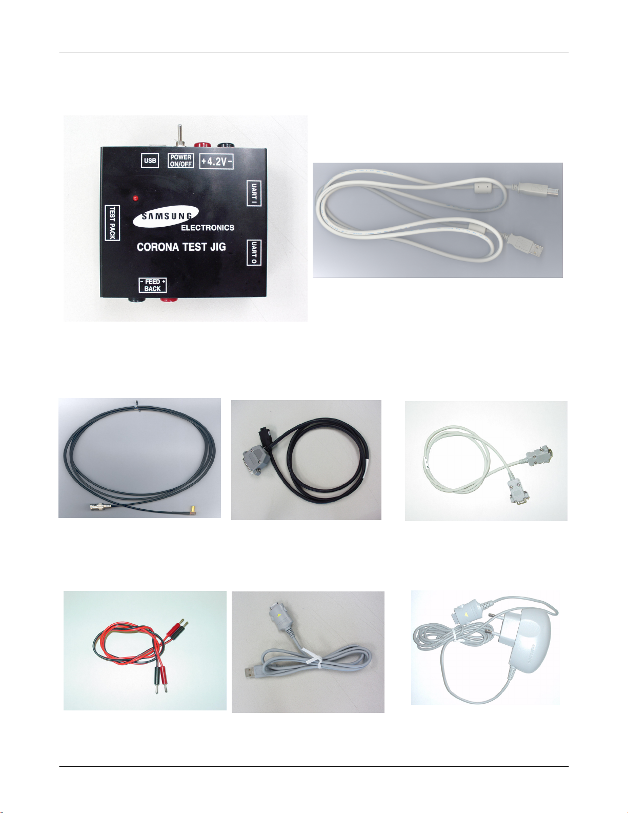
3-3. Test Jig (GH80-03306A)
3-3-2. RF Test Cable
(GH39-00283A)
3-3-3. Test Cable
3-3-1. USB JIG Cable
(GH39-00337A)
3-3-4. Serial Cable
(CSA LL64151-A)
3-3-5. Power Supply Cable
SAMSUNG Proprietary-Contents may change without notice
This Document can not be used without Samsung's authorization
3-3-6. DATA CABLE
(GH39-00331A]
3-4
3-3-7. TA
(GH44-00482A)

4. Electrical Parts List
Design LOC Description SEC CODE STATUS
ANT1 NPR-ANTENNA CONTACT GH71-04302A SA
ANT2 NPR-ANTENNA CONTACT GH71-04302A SA
ANT300 ANTENNA-CHIP 4202-001099 SA
AR201 R-NET 2011-001394 SA
BAT400 BATTERY-LI(2ND) 4302-001181 SA
BTC501 CONNECTOR-BATTERY 3711-005829 SA
C101 C-CER,CHIP 2203-000278 SA
C102 C-CER,CHIP 2203-000278 SA
C104 C-CER,CHIP 2203-000278 SA
C105 C-CER,CHIP 2203-000278 SA
C106 C-CER,CHIP 2203-000812 SA
C107 C-CER,CHIP 2203-001072 SA
C109 C-CER,CHIP 2203-000278 SA
C110 C-CER,CHIP 2203-000278 SA
C112 C-CER,CHIP 2203-000812 SA
C113 C-CER,CHIP 2203-000233 SA
C114 C-CER,CHIP 2203-000233 SA
C115 C-CER,CHIP 2203-000812 SA
C116 C-CER,CHIP 2203-000233 SA
C117 C-CER,CHIP 2203-000812 SA
C118 C-CER,CHIP 2203-000233 SA
C119 C-CER,CHIP 2203-000812 SA
C121 C-CER,CHIP 2203-000812 SA
C122 C-CER,CHIP 2203-000254 SA
C123 C-CER,CHIP 2203-000278 SA
C124 C-CER,CHIP 2203-005281 SA
C125 C-CER,CHIP 2203-005281 SA
C126 C-CER,CHIP 2203-000233 SA
C127 C-CER,CHIP 2203-000278 SA
C130 C-CER,CHIP 2203-000854 SA
C131 C-CER,CHIP 2203-000854 SA
C132 C-CER,CHIP 2203-000254 SA
C134 C-CER,CHIP 2203-005052 SA
C136 C-CER,CHIP 2203-000530 SA
C137 C-CER,CHIP 2203-000233 SA
C142 C-CER,CHIP 2203-001072 SA
C201 C-CER,CHIP 2203-005482 SA
C202 C-CER,CHIP 2203-005482 SA
C203 C-CER,CHIP 2203-000254 SA
C204 C-CER,CHIP 2203-005482 SA
C205 C-CER,CHIP 2203-005482 SA
C206 C-CER,CHIP 2203-000812 SA
C207 C-CER,CHIP 2203-005482 SA
C208 C-CER,CHIP 2203-005482 SA
C209 C-CER,CHIP 2203-005482 SA
C210 C-CER,CHIP 2203-005482 SA
C211 C-CER,CHIP 2203-005482 SA
C212 C-CER,CHIP 2203-005482 SA
C213 C-CER,CHIP 2203-005482 SA
C214 C-CER,CHIP 2203-000812 SA
SAMSUNG Proprietary-Contents may change without notice
This Document can not be used without Samsung's authorization
4-1

Electrical Parts List
Design LOC Description SEC CODE STATUS
C215 C-CER,CHIP 2203-005482 SA
C216 C-CER,CHIP 2203-005482 SA
C217 C-CER,CHIP 2203-006190 SA
C218 C-CER,CHIP 2203-006190 SA
C301 C-CER,CHIP 2203-000254 SA
C302 C-CER,CHIP 2203-005482 SA
C303 C-CER,CHIP 2203-005482 SA
C304 C-CER,CHIP 2203-000233 SA
C305 C-CER,CHIP 2203-000679 SA
C306 C-CER,CHIP 2203-005482 SA
C307 C-CER,CHIP 2203-005482 SA
C308 C-CER,CHIP 2203-000438 SA
C309 C-CER,CHIP 2203-006348 SA
C310 C-CER,CHIP 2203-005482 SA
C311 C-CER,CHIP 2203-000438 SA
C312 C-CER,CHIP 2203-005482 SA
C313 C-CER,CHIP 2203-005512 SA
C315 C-CER,CHIP 2203-000679 SA
C316 C-CER,CHIP 2203-006562 SA
C317 C-CER,CHIP 2203-006562 SA
C319 C-CER,CHIP 2203-005482 SA
C320 C-CER,CHIP 2203-006562 SA
C321 C-CER,CHIP 2203-006562 SA
C322 C-CER,CHIP 2203-005482 SA
C323 C-CER,CHIP 2203-005482 SA
C401 C-CER,CHIP 2203-000359 SA
C402 C-CER,CHIP 2203-006208 SA
C403 C-CER,CHIP 2203-006201 SA
C404 C-CER,CHIP 2203-006562 SA
C405 C-CER,CHIP 2203-006324 SA
C406 C-CER,CHIP 2203-000386 SA
C407 C-CER,CHIP 2203-006257 SA
C408 C-CER,CHIP 2203-000386 SA
C409 C-CER,CHIP 2203-006257 SA
C410 C-CER,CHIP 2203-000233 SA
C412 C-CER,CHIP 2203-000812 SA
C413 C-CER,CHIP 2203-006208 SA
C414 C-CER,CHIP 2203-006399 SA
C415 C-CER,CHIP 2203-006208 SA
C416 C-CER,CHIP 2203-006257 SA
C417 C-CER,CHIP 2203-006257 SA
C419 C-CER,CHIP 2203-006208 SA
C420 C-CER,CHIP 2203-005482 SA
C422 C-CER,CHIP 2203-006208 SA
C423 C-CER,CHIP 2203-006208 SA
C424 C-CER,CHIP 2203-006257 SA
C425 C-CER,CHIP 2203-006257 SA
C501 C-CER,CHIP 2203-002443 SA
C502 C-CER,CHIP 2203-006399 SA
C503 C-CER,CHIP 2203-000812 SA
4-2
SAMSUNG Proprietary-Contents may change without notice
This Document can not be used without Samsung's authorization

Electrical Parts List
Design LOC Description SEC CODE STATUS
C504 C-CER,CHIP 2203-005482 SA
C505 C-CER,CHIP 2203-005482 SA
C506 C-CER,CHIP 2203-005482 SA
C507 C-CER,CHIP 2203-006562 SA
C508 C-CER,CHIP 2203-000812 SA
C552 C-CER,CHIP 2203-000233 SA
C601 C-CER,CHIP 2203-000643 SA
C602 C-CER,CHIP 2203-000278 SA
C604 C-CER,CHIP 2203-005482 SA
C605 C-CER,CHIP 2203-002668 SA
C606 C-CER,CHIP 2203-000995 SA
C607 C-CER,CHIP 2203-005482 SA
C608 C-CER,CHIP 2203-000278 SA
C612 C-CER,CHIP 2203-000254 SA
C613 C-CER,CHIP 2203-000995 SA
C614 C-CER,CHIP 2203-000278 SA
C615 C-CER,CHIP 2203-003054 SA
C616 C-CER,CHIP 2203-006137 SA
C617 C-CER,CHIP 2203-003054 SA
C629 C-CER,CHIP 2203-006137 SA
C630 C-CER,CHIP 2203-000995 SA
C701 C-CER,CHIP 2203-006201 SA
C702 C-CER,CHIP 2203-006438 SA
C703 C-CER,CHIP 2203-005482 SA
C704 C-CER,CHIP 2203-005482 SA
C705 C-CER,CHIP 2203-000812 SA
C706 C-CER,CHIP 2203-000812 SA
C708 C-CER,CHIP 2203-000812 SA
C709 C-CER,CHIP 2203-000812 SA
C729 C-CER,CHIP 2203-005249 SA
C730 C-CER,CHIP 2203-006137 SA
C731 C-CER,CHIP 2203-000679 SA
EAR600 JACK-PHONE 3722-002082 SA
F101 DUPLEXER-ASM 2911-000018 SA
F102 FILTER-EMI SMD 2901-001254 SA
F103 FILTER-SAW 2904-001553 SA
F701 FILTER-EMI SMD 2901-001286 SA
F702 FILTER-EMI SMD 2901-001286 SA
F703 FILTER-EMI SMD 2901-001286 SA
F704 FILTER-EMI SMD 2901-001286 SA
F705 FILTER-EMI SMD 2901-001286 SA
IFC500 CONNECTOR-INTERFACE 3710-001994 SA
L105 INDUCTOR-SMD 2703-002281 SA
L106 INDUCTOR-SMD 2703-002314 SA
L108 INDUCTOR-SMD 2703-002313 SA
L109 INDUCTOR-SMD 2703-002309 SA
L110 INDUCTOR-SMD 2703-002485 SA
L111 INDUCTOR-SMD 2703-001752 SA
L112 INDUCTOR-SMD 2703-002267 SA
L114 BEAD-SMD 3301-001729 SA
4-3
SAMSUNG Proprietary-Contents may change without notice
This Document can not be used without Samsung's authorization
Electrical Parts List
Design LOC Description SEC CODE STATUS
L115 INDUCTOR-SMD 2703-002268 SA
L117 INDUCTOR-SMD 2703-002268 SA
L200 BEAD-SMD 3301-001789 SA
L301 INDUCTOR-SMD 2703-001752 SA
L401 BEAD-SMD 3301-001120 SA
L402 INDUCTOR-SMD 2703-002653 SA
L501 BEAD-SMD 3301-001534 SA
L601 BEAD-SMD 3301-001534 SA
L602 BEAD-SMD 3301-001534 SA
L603 INDUCTOR-SMD 2703-001231 SA
L604 INDUCTOR-SMD 2703-002198 SA
L607 INDUCTOR-SMD 2703-002198 SA
L613 INDUCTOR-SMD 2703-002308 SA
L614 INDUCTOR-SMD 2703-002308 SA
L617 INDUCTOR-SMD 2703-002308 SA
L703 INDUCTOR-SMD 2703-001673 SA
LED701 LED 0601-002037 SA
LED702 LED 0601-002037 SA
LED703 LED 0601-002037 SA
LED704 LED 0601-002037 SA
LED705 LED 0601-002037 SA
LED706 LED 0601-002037 SA
LED707 LED 0601-002037 SA
LED708 LED 0601-002037 SA
LED709 LED 0601-002037 SA
LED710 LED 0601-002037 SA
LED711 LED 0601-002037 SA
LED712 LED 0601-002037 SA
MOD301 BLUETOOTH MODULE 4709-001377 SA
OSC101 OSCILLATOR-VCTCXO 2809-001281 SA
OSC400 CRYSTAL-SMD 2801-004466 SA
PAM101 IC-POWER AMP 1201-002280 SA
R103 R-CHIP 2007-000171 SA
R104 R-CHIP 2007-000171 SA
R107 R-CHIP 2007-000148 SA
R108 R-CHIP 2007-000172 SA
R109 R-CHIP 2007-000566 SA
R110 R-CHIP 2007-003001 SA
R111 R-CHIP 2007-000566 SA
R112 R-CHIP 2007-000171 SA
R113 R-CHIP 2007-000932 SA
R114 R-CHIP 2007-000932 SA
R115 R-CHIP 2007-000171 SA
R116 R-CHIP 2007-000140 SA
R117 R-CHIP 2007-001288 SA
R118 R-CHIP 2007-001313 SA
R119 R-CHIP 2007-001313 SA
R120 R-CHIP 2007-000171 SA
R121 R-CHIP 2007-000171 SA
R122 R-CHIP 2007-000171 SA
4-4
SAMSUNG Proprietary-Contents may change without notice
This Document can not be used without Samsung's authorization

Electrical Parts List
Design LOC Description SEC CODE STATUS
R123 R-CHIP 2007-000171 SA
R124 R-CHIP 2007-000171 SA
R125 R-CHIP 2007-000171 SA
R201 R-CHIP 2007-000171 SA
R202 R-CHIP 2007-000148 SA
R203 R-CHIP 2007-000171 SA
R204 R-CHIP 2007-000162 SA
R206 R-CHIP 2007-007137 SA
R207 R-CHIP 2007-007137 SA
R209 R-CHIP 2007-000162 SA
R210 R-CHIP 2007-000143 SA
R211 R-CHIP 2007-000171 SA
R212 R-CHIP 2007-000171 SA
R215 R-CHIP 2007-000171 SA
R301 R-CHIP 2007-000171 SA
R302 R-CHIP 2007-007014 SA
R303 R-CHIP 2007-001303 SA
R304 R-CHIP 2007-000157 SA
R305 R-CHIP 2007-001325 SA
R306 R-CHIP 2007-000151 SA
R307 R-CHIP 2007-001323 SA
R308 R-CHIP 2007-000143 SA
R309 R-CHIP 2007-000162 SA
R310 R-CHIP 2007-000162 SA
R311 R-CHIP 2007-000141 SA
R312 R-CHIP 2007-000141 SA
R313 R-CHIP 2007-000162 SA
R314 R-CHIP 2007-000148 SA
R315 R-CHIP 2007-000171 SA
R401 R-CHIP 2007-000171 SA
R402 R-CHIP 2007-007100 SA
R403 R-CHIP 2007-000171 SA
R404 R-CHIP 2007-000162 SA
R405 R-CHIP 2007-002796 SA
R407 R-CHIP 2007-008812 SA
R408 R-CHIP 2007-007107 SA
R409 R-CHIP 2007-000162 SA
R501 R-CHIP 2007-000162 SA
R502 R-CHIP 2007-000171 SA
R503 R-CHIP 2007-000758 SA
R504 R-CHIP 2007-000162 SA
R505 R-CHIP 2007-000162 SA
R507 R-CHIP 2007-000152 SA
R508 R-CHIP 2007-000170 SA
R509 R-CHIP 2007-000170 SA
R510 R-CHIP 2007-007573 SA
R511 R-CHIP 2007-000137 SA
R512 R-CHIP 2007-007334 SA
R513 R-CHIP 2007-000164 SA
R514 R-CHIP 2007-000156 SA
4-5
SAMSUNG Proprietary-Contents may change without notice
This Document can not be used without Samsung's authorization

Electrical Parts List
Design LOC Description SEC CODE STATUS
R515 R-CHIP 2007-007489 SA
R541 R-CHIP 2007-000171 SA
R603 R-CHIP 2007-000242 SA
R605 R-CHIP 2007-000148 SA
R606 R-CHIP 2007-000242 SA
R607 R-CHIP 2007-002796 SA
R608 R-CHIP 2007-007573 SA
R609 R-CHIP 2007-000831 SA
R610 R-CHIP 2007-000162 SA
R611 R-CHIP 2007-007480 SA
R615 R-CHIP 2007-000162 SA
R616 R-CHIP 2007-001339 SA
R619 R-CHIP 2007-000171 SA
R701 R-CHIP 2007-002970 SA
R702 R-CHIP 2007-002970 SA
R703 R-CHIP 2007-002970 SA
R704 R-CHIP 2007-002970 SA
R705 R-CHIP 2007-002970 SA
R706 R-CHIP 2007-000172 SA
R707 R-CHIP 2007-002970 SA
R708 R-CHIP 2007-000172 SA
R709 R-CHIP 2007-002970 SA
R710 R-CHIP 2007-002970 SA
R711 R-CHIP 2007-000172 SA
R712 R-CHIP 2007-002970 SA
R714 R-CHIP 2007-000171 SA
R715 R-CHIP 2007-000162 SA
R716 R-CHIP 2007-000171 SA
R718 R-CHIP 2007-000172 SA
R719 R-CHIP 2007-000172 SA
R732 R-CHIP 2007-000171 SA
R733 R-CHIP 2007-000171 SA
R734 R-CHIP 2007-000148 SA
R735 R-CHIP 2007-000758 SA
R736 R-CHIP 2007-000171 SA
R737 R-CHIP 2007-000138 SA
RFS101 CONNECTOR-COAXIAL 3705-001358 SA
SIM400 CONNECTOR-CARD EDGE 3709-001355 SA
SOC701 HEADER-BOARD TO BOARD 3711-005918 SA
TA101 C-TA,CHIP 2404-001411 SA
TA401 C-TA,CHIP 2404-001394 SA
TA501 C-TA,CHIP 2404-001394 SA
TA502 C-TA,CHIP 2404-001394 SA
TA601 C-TA,CHIP 2404-001402 SA
TAC701 SWITCH-TACT 3404-001152 SA
U102 IC-TRANSCEIVER 1205-002817 SA
U300 IC-MELODY 1204-002161 SA
U301 IC-CMOS LOGIC 0801-003022 SA
U302 IC-CMOS LOGIC 0801-003025 SA
U305 FET-SILICON 0505-001923 SA
4-6
SAMSUNG Proprietary-Contents may change without notice
This Document can not be used without Samsung's authorization
 Loading...