

Samsung SGH-E330N Service Manual
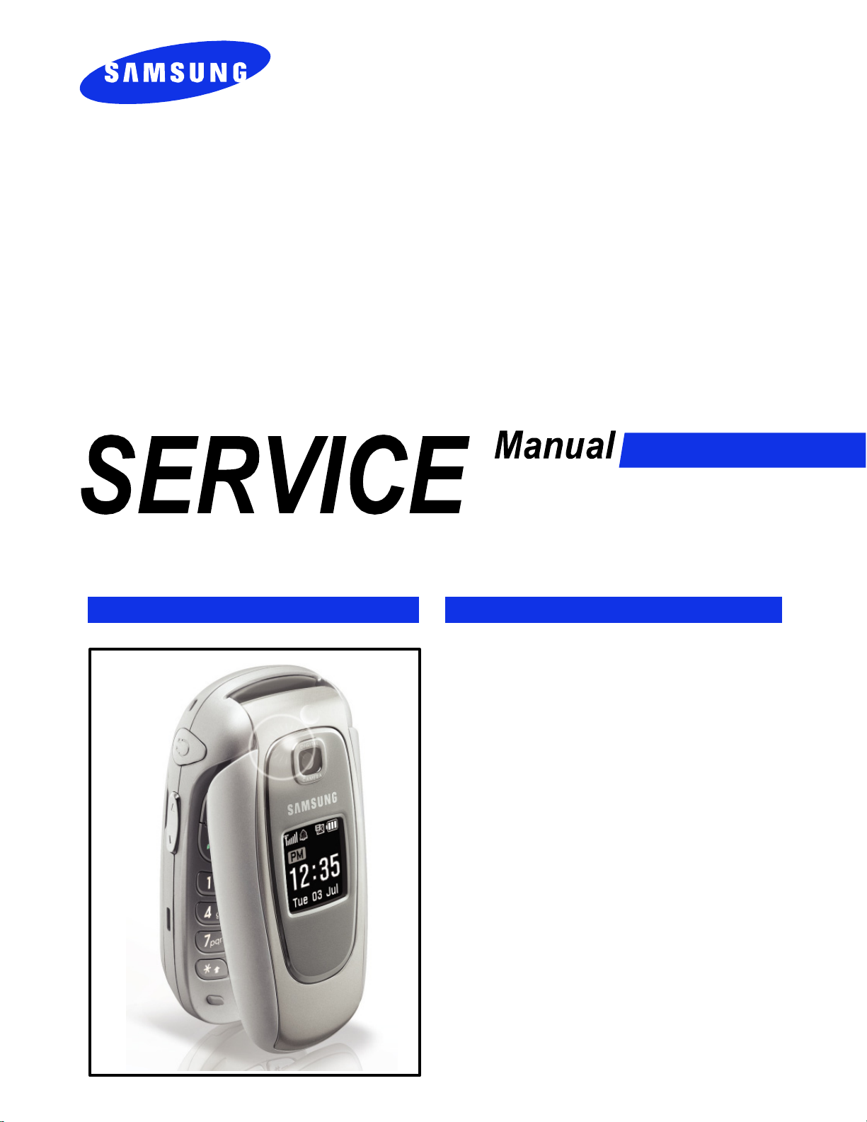
GSM TELEPHONE
SGH-E330N
GSM TELEPHONE
CONTENTS
1. Specification
2. Circuit Description
3. Exploded Views and Parts List
4. Electrical Parts List
5. Block Diagrams
6. PCB Diagrams
7. Flow Chart of Troubleshooting

This Service Manual is a property of Samsung Electronics Co.,Ltd.
Any unauthorized use of Manual can be punished under applicable
International and/or domestic law.
ⓒ
Samsung Electronics Co.,Ltd. October. 2005
Printed in Korea.
Code No.: GH68-08696A
BASIC.
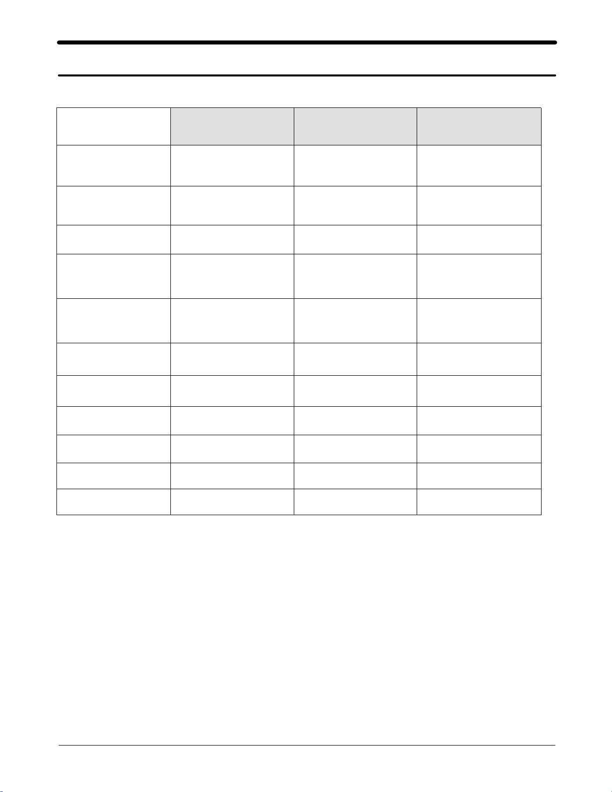
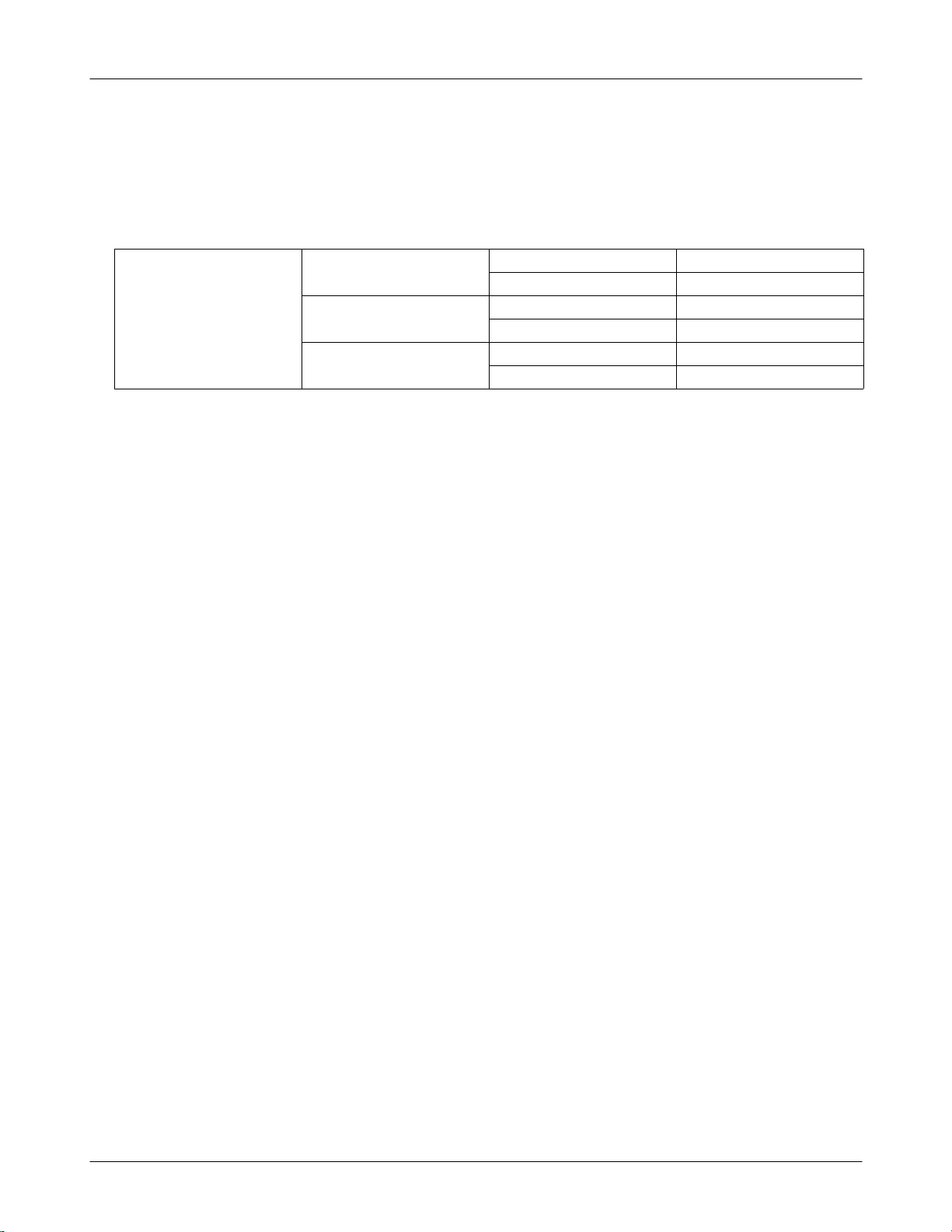
1. Specification
1-1. GSM General Specification
GSM900
Phase 1
Freq. Band[MHz]
Uplink/Downlink
ARFCN range 1~124 512~885 512~810
Tx/Rx spacing 45MHz 95MHz 80MHz
Mod. Bit rate/
Bit Period
Time Slot
Period/Frame Period
Modulation 0.3GMSK 0.3GMSK 0.3GMSK
MS Power 33dBm~5dBm 30dBm~0dBm 30dBm~0dBm
890~915
935~960
270.833kbps
3.692us
576.9us
4.615ms
DCS1800
Phase 1
1710~1785
1805~1880
270.833kbps
3.692us
576.9us
4.615ms
Phase 1
1850~1910
1930~1990
270.833kbps
4.615ms
PC1900
3.692us
576.9us
Power Class 5pcl ~ 19pcl 0pcl ~ 15pcl 0pcl ~ 15pcl
Sensitivity -102dBm -100dBm -100dBm
TDMA Mux 8 8 8
Cell Radius 35Km 2Km -
1-1
SAMSUNG Proprietary-Contents may change without notice
This Document can not be used without Samsung's authorization
Specification
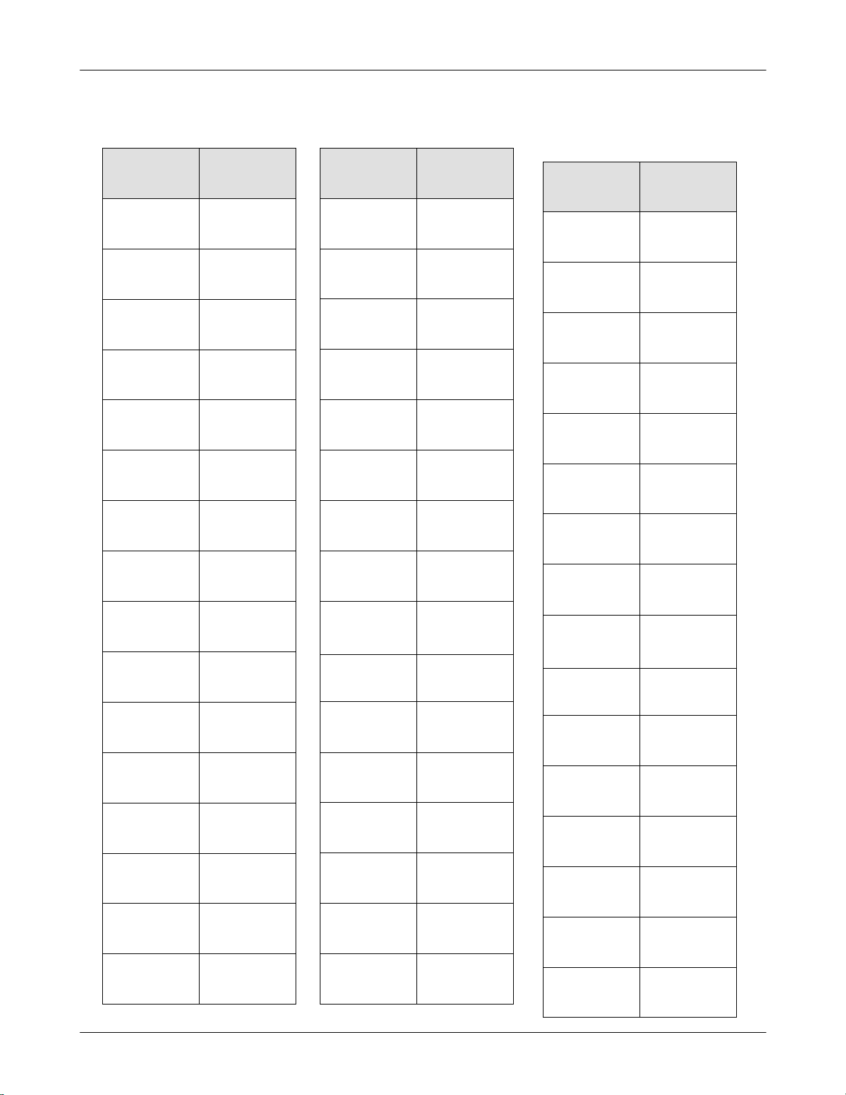
1-2. GSM TX power class
TX Power
control level
5 33±3 dBm
6 31±3 dBm
7 29±3 dBm
8 27±3 dBm
9 25±3 dBm
10 23±3 dBm
11 21±3 dBm
GSM900
TX Power
control level
0 30±3 dBm
1 28±3 dBm
2 26±3 dBm
3 24±3 dBm
4 22±3 dBm
5 20±3 dBm
6 18±3 dBm
DCS1800
TX Power
control level
0 30±3 dBm
1 28±3 dBm
2 26±3 dBm
3 24±3 dBm
4 22±3 dBm
5 20±3 dBm
6 18±3 dBm
PCS1900
12 19±3 dBm
13 17±3 dBm
14 15±3 dBm
15 13±3 dBm
16 11±5 dBm
17 9±5dBm
18 7±5 dBm
19 5±5 dBm
7 16±3 dBm
7 16±3 dBm
8 14±3 dBm
8 14±3 dBm
9 12±4 dBm
9 12±4 dBm
10 10±4 dBm
10 10±4 dBm
11 8±4dBm
11 8±4dBm
12 6±4 dBm
12 6±4 dBm
13 4±4 dBm
13 4±4 dBm
14 2±5 dBm
14 2±5 dBm
15 0±5 dBm
1-2
15 0±5 dBm
SAMSUNG Proprietary-Contents may change without notice
This Document can not be used without Samsung's authorization
2. Circuit Description
2-1. SGH-E330N RF Circuit Description
2-1-1. RX PART
- ASM(U103)→Switching Tx, Rx path for GSM900, DCS1800, PCS1900 by logic controlling.
- ASM Control Logic (U103)
GSM Tx Mode H L L
DCS Tx Mode L H L
PCS Tx Mode H L L
GSM Rx Mode L L L
DCS Rx Mode L L L
PCS Rx Mode L L H
- FILTER
To convert Electromagnetic Field Wave to Acoustic Wave and then pass the specific frequency band.
- GSM FILTER (F100)→For filtering the frequency band between 869 and 894 MHz
- DCS FILTER (F102)→For filtering the frequency band between 1805 and 1880 MHz.
- PCS FILTER (F101)→For filtering the frequency band between 1930 and 1990 MHz.
- VC-TCXO (OSC100)
This module generates the 26MHz reference clock to drive the logic and RF. After division by two a reference clock of
13MHz is supplied to the other parts of the system through the pin CLKOUT. After additional process, the reference
clock applies t o the U100 Rx IQ demodulator and Tx IQ modulator. And then, the oscillator is controlled by serial data
to select channel and use fast lock mode for GPRS high class operation.
→
Truth Table
VC1 VC2 VC3
- Transceiver (U100)
The receiver front-end which amplifies the GSM, DCS aerial signal, converts the chosen channel down to a low IF signal
of 100 kHz. The first stages are symmetrical low noise amplifiers (LNAs). The LNAs are followed by an IQ down mixer.
It consists of two mixers in parallel but driven by quadrature out of phase LO signals. The In phase (I) and Quadrature
phase (Q) IF signals are low pass filtered to provide protection from high frequency offset interferes. The low IF I and Q
signals are then fed into the channel filter. The front-end low IF I and Q outputs enter the integrated bandpass channel
filter with provision for five 8 dB gain steps in front of the filter.
2-1-2. TX PART
I and Q baseband signals are applied to the IQ modulator that shifts the modulation spectrum up to the transmit IF. It is
designed for low harmonic distortion, low carrier leakage and high image rejection to keep the phase error as small as
possible.
2-1
SAMSUNG Proprietary-Contents may change without notice
This Document can not be used without Samsung's authorization
Circuit Description
The modulator is loaded at its IF output by an integrated low pass filter that suppress unwanted spurs prior to get into
the phase detector. The clock drive is generated by division of the RFLO signal provided for the transmit offset mixer.
Baseband IQ signal fed into offset PLL, this function is included inside of U100 chip. OSC101 chip generates modulator
signal which power level is about 6.5dBm and fed into Power Amplifier(U102). The PA output power and power ramping
are well controlled by Auto Power Control circuit. We use offset PLL below table.
GSM -35dBc
DCS -35dBc
GSM -66dBc
DCS -65dBc
GSM -75dBc
DCS -68dBc
Modulation Spectrum
200kHz offset
30 kHz bandwidth
400kHz offset
30 kHz bandwidth
600kHz ~ 1.8MHz offset
30 kHz bandwidth
2-2. Baseband Circuit description of SGH-E330N
2-2-1. PCF50601
- Power Management
Ten low-dropout regulators designed specifically for GSM applications power the terminal and help ensure optimal system
performance and long battery life. A programmable boost converter provides support for 1.8V, 3.0V, and 5.0V SIMs,
while a self-resetting, electronically fused switch supplies power to external accessories. Ancillary support functions, such
as RTC module and High Voltage Charge pump, Clock generator, aid in reducing both board area and system complexity.
I2C BUS serial interface provides access to control and configuration registers. This interface gives a microprocessor full
control of the PCF50601 and enables system designers to maximize both standby and talk times.
Supervisory functions. including a reset generator, an input voltage monitor, and a temperature sensor, support reliable
system design. These functions work together to ensure proper system behavior during start-up or in the event of a fault
condition(low microprocessor voltage, insufficient battery energy, or excessive die temperature).
Backlight Brightness Modulator
-
The Backlight Brightness Modulator (BBM) contains a programmable Pulse-width
to modulate the intensity of a series of LED’s or to control a DC/DC converter that drives LCD backlight.
But, this phone (SGH-E330N) is use UFB LCD. UFB LCD controls backlight brightness by contrast setting.
So "BL_VDD" voltage is always high value when phone is in active mode. When phone is in dimming mode "BL_VDD"
goes to about 10% duty PWM.
Clock Generato
-
The Clock Generator (CG) generates all clocks for internal and external usage. The 32768 Hz crystal
oscillator provides an accurate low clock frequency for the PCF50601 and other circuitry.
r
modulator (PWM) and FET
2-2-2. LCD Connector
LCD is consisted of main LCD(color 65K UFB LCD) and sub LCD (4Gray LCD).
Chip select signals LCD_MAIN_CS and LCD_SUB_CS, can enable Each LCD. BACKLIGHT signal enables white LED
of main LCD. "RESET_2V8" signal initiates the reset process of the LCD.
2-2
SAMSUNG Proprietary-Contents may change without notice
This Document can not be used without Samsung's authorization

Circuit Description
16-bit data lines(LD(0)~LD(15)) transfers data and commands to LCD through bypass capacitor. Data and commands use
"RS" signal. If this signal is high, inputs to LCD are commands. If it is low, inputs to LCD are data.
The signal which informs the state of LCD is whether input or output, is required. But in this system, there is no input
state from LCD. So only "L_WR" signal is used to indicate write data or command to LCD. Power signals for LCD are
"VBAT and "VDD2".
"M_SCL", "M_SCA", "PCLK", "FVALID", "LVALID" and "STANDBY" signals are all related to camera working.
"CAMERA_FLASH_SUPPLY" is voltage supply to flash led , and "SVC_LED" is signal for service led when the signal
is low led is on and vice versa. "SPK_P" and "SPK_N" are used for audio speaker containing voice or melody. And
"VDD_VIB" from PCF50601 enables the motor.
2-2-3. Key
This is consisted of key interface pins among OM6359, KBIO(0:7). These signals compose the matrix. Result of matrix
informs the key status to key interface in the OM6359. Power on/off key is separated from the matrix. So power on/off
signal is connected with PCF50601 to enable PCF50601. Fifteen key LEDs are use the "VBAT" as supply voltage.
"VDD_KEY" signal enables LEDs. "FLIP" informs the status of folder (open or closed) to the OM6359. This uses the
hall effect IC, SH248CSP. A magnet under main LCD enables SH248CSP.
2-2-4. EMI ESD Filter
This system uses the EMI ESD filter, EMIF09 to protect noise from IF CONNECTOR part.
2-2-5. IF connetor
It is 18-pin connector. They are designed to use VBAT, V_EXT_CHARGE, TXD0, RXD0, RTS0, CTS0, JIG_REC,
CHARGER_OK, RXD1, TXD1, AUX_MIC, AUX_SPK and GND. They connected to power supply IC, microprocessor
and signal processor IC.
2-2-6. Battery Charge Management
A complete constant-current/constant-voltage linear charger is used for single cell lithium-ion batteries.
If TA connected to phone, "V_EXT_CHARGE" enable charger IC and supply curre nt to battery.
When fault condition caused, "CHG_ON" signal level change low to high and charger IC stop charging
process.
2-2-7. Audio
EARP_P and EARP_N from OM6359 are connected to the main speaker. AUXSP is connected to the Hands free kit.
MIC_P and MIC_N are connected to the main MIC. And AUX_MIC_P and AUX_MIC_N are connected to the Hands
free kit.
YMU762C is a LSI for portable telephone that is capable of playing high quality music by utilizing FM synthesizer and
ADPCM decoder that are included in this device.
As a synthesis, YMU762C is equipped 32 voices with different tones. Since the device is capable of simultaneously
generating up to synchronous with the play of the FM synthesizer, various sampled voices can be used as sound effects.
Since the play data of YMU762C are interpreted at anytime through FIFO, the length of the data(playing period) is not
limited, so the device can flexibly support application such as incoming call melody music distribution service. The
hardware sequencer built in this device allows playing of the complex music without giving excessive load to the CPU of
the portable telephones.
2-3
SAMSUNG Proprietary-Contents may change without notice
This Document can not be used without Samsung's authorization

Circuit Description
Moreover, the registers of the FM synthesizer can be operated directly for real time sound generation, allowing, for
example, utilization of various sound effects when using the game software installed in the portable telephone.
YMU762C includes a speaker amplifier with high ripple removal rate whose maximum output is 550mW (SPVDD=3.6V).
The device is also equipped with conventional function including a vibrator and a circuit for controlling LEDs
synchronous with music.
For the headphone, it is provided with a stereophonic output terminal.
For the purpose of enabling YMU762C to demonstrate its full capabilities, Yamaha purpose to use "SMAF:Synthetic music
Mobile Application Format" as a data distribution format that is compatible with multimedia. Since the SMAF takes a
structure that sets importance on the synchronization between sound and images, various contents can be written into it
including incoming call melody with words that can be used for training karaoke, and commercial channel that combines
texts, images and sounds, and others. The hardware sequencer of YMU762C directly interprets and plays blocks relevant
to synthesis (playing music and reproducing ADPCM with FM synthesizer) that are included in data distributed in SMAF.
2-2-8. Memory
Signals in the OM6359 enable two memories. They use only one volt supply voltage, VDD3 in the PCF50601. This
system uses Samsung's memory, KBB06A500M-T402. It is consisted of 128M bits flash NOR memory and 128M bits
flash NAND memory and 64M bits SCRAM. It has 16 bit data line, HD[0~15] which is connected to OM6359 and
MV317S. It has 26 bit address lines, HA[1~26]. CS_NAND and NCSRAM signals are chip select. Writing process,
HWR_N is low and it enables writing process to flash memory and SRAM. During reading process, HRD_N is low and
it enables reading process to flash memory and SRAM. Each chip select signals in the OM6359 select memory among 2
flash memory and SCRAM. Reading or writing procedure is processed after HWR_N or HRD_N is enabled. Memories
use reset, which is VDD3 delay from PCF50601. HA[25] signal enables lower byte of SRAM and HA[26] signal enables
higher byte of SRAM.
2-2-9. OM6359
OM6359 is consisted of ARM core and DSP core. It has
on-chip program ROM
of KBS, JTAG, EMI and UART. ARM core is consisted of EMI, PIC(Programmable Interrupt Controller),
reset/power/clock unit, DMA controller, TIC(Test Interface Controller), peripheral bridge, PPI, SSI(Synchronous Serial
Interface), ACC(Asynchronous communications controllers), timer, ADC, RTC(Real-Time Clock) and keyboard interface.
KBIO(0:7), address lines of DSP core and HD[0~15]. HA[1~26], address lines of ARM core and HD[0~15], data lines of
ARM core are connected to memory, YMU762C. MV317S(Camera DSP Chip) controls the communication between ARM
core and DSP core.
CS_NAND, NCSRAM, NCSFLASH in the ARM core are connected to each memory. HWR_N and HRD_N control the
process of memory. External IRQ(Interrupt ReQuest) signals from each units, such as, PMU need the compatible process.
KBIO[0~7] receive the status from key and RXD0/TXD0 are used for the communication using data link
cable(DEBUG_DTR/RTS/TXD/RXD/CTS/DSR).
It has JTAG control pins(TDI/TDO/TCK) for ARM core and DSP core. It receives 13MHz clock in CKI pin from
external TCXO. ADC(Analog to Digital Convertor) part receives the status of temperature, battery type and battery voltage.
in the DSP. It has 4K*32bits ROM and 2K*32bits RAM in the ARM core. DSP is consisted
8x1Kword on-chip program/data RAM, 55 Kwords
2-4
SAMSUNG Proprietary-Contents may change without notice
This Document can not be used without Samsung's authorization

Circuit Description
2-2-10. TOH2600DGI4KRA(26MHz)
This system uses the 26MHz TCXO, TOH2600DGI4KRA, SEM. AFC control signal from OM6359 controls frequency
from 26MHz x-tal. The clock output frequency of UAA3536 is 13MHz. This clock is connected to OM6359, YMU762C.
2-2-11. Camera DSP(MV3018SAQ)
MV3018 is a Camera Control Processor providing the most efficient camera functions for portable terminal devices such
as mobile handsets. MV3018 provides rich video functions up to 30-frame display with minimized tasks in the handset
main processor as well as hardware based real-time JPEG compression and decompression. MV3018 directly transmits and
previews the RGB data to the LCD graphic memory by processing the sensor output data according to the cell phone's
command. MV3018 can allow the host processor to download with scalable sized compressed data. In addition, MV3018
can download the compressed image to either store the original RGB data or transfer the image to the LCD. This feature
allows the main processor to minimize its function while obtaining the result of the image process. MV3018 can support
sensors up to 300K pixels.
The main processor to minimize its function while obtaining the result of the image process. MV3018 can support sensors
up to VGA pixels.
2-5
SAMSUNG Proprietary-Contents may change without notice
This Document can not be used without Samsung's authorization

Circuit Description
2-6
SAMSUNG Proprietary-Contents may change without notice
This Document can not be used without Samsung's authorization

3. Exploded Views and Parts List
3-1. Exploded View
QWD02
QFR01
QSC14
QMI03
QKP01
QFU01
QLC01
QMO01
QSP01
QFL01
QCR53
QCA01
QSC08
QRF03
QVO01
QIF01
QME01
QMP01
QMI01
QCR08
QAN02
QRE01
QCK01
QRF01
QCR21
QMW02
QBA19
3-1
SAMSUNG Proprietary-Contents may change without notice
This Document can not be used without Samsung's authorization
Exploded Views and Parts List
3-2. Parts List
Location No Description SEC Code
QAN02
QBA19
QCA01
QCK01
QCR08
QCR21
QCR53
QFL01
QIF01
QKP01
QLC01
QME01
QMI01
QMO01
QMP01
QMW02
ㅤ
ㅤ
ㅤ
ㅤ
ㅤ
ㅤ
ㅤ
ㅤ
ㅤ
ㅤ
ㅤ
ㅤ
ㅤ
ㅤ
ㅤ
ㅤ
INTENNA-SGHE330N;IAPT0GDP3815SC,SGH- GH42-00623A
BATTERY-800MAH,ANT SIL,EU,M;BST5068S GH43-01988A
UNIT-CAMERA;SGH-E335,MOMFH150G2A,-,U GH59-02050A
MEC-CAMERA KEY ASSY;SGH-X640,XEF,-,- GH75-06567A
SCREW-MACHINE;CH,+,M1.4,L3,BLK,SWRCH 6001-001456
SCREW-MACHINE;BH(1.0),+,M1.7,L3.5,BL 6001-001507
SCREW-MACHINE;CH,+,M1.7,L5,ZPC(BLK), 6001-001639
MEC-FOLDER LOWER;SGH-E330N,EU,-,-,-, GH75-07535A
PMO-IF COVER;SGH-E330N,PC+RUBBER,SIL GH72-23262A
MEC-KEYPAD;SGH-E330N,EU,-,-,-,-,SIL, GH75-07639A
LCD-SGHE335 MAIN MODULE;UG-12R110-C, GH07-00689A
UNIT-METAL DOME;SGH-E330N,-,-,XET,12 GH59-02405A
MICROPHONE-ASSY;2,130~500uA,-44dB,2. GH30-00130A
MOTOR-DC;12000rpm,0g.cm,3V,80mA 3101-001401
PBA MAIN-SGHE330N;SGH-E330N,XEF,UNKD GH92-02281A
PCT-MAIN WINDOW;SGH-E330N,ACRYLIC,TR GH72-23488A
QRE01
QRF01
QSC08
QSC14
QSP01
QVO01
QFU01
ㅤ
QFR01
ㅤ
ㅤ
ㅤ
ㅤ
ㅤ
ㅤ
ㅤ
ㅤ
ㅤ
QWD02 PCT-WINDOW DUAL;SGH-E335,ACRYL,TRP,- GH72-19294A
ㅤ
QRF03 PMO-EAR COVER;SGH-E330N,PC,SIL,-,-,- GH72-19199F
QMI03 RMO-MIC RUBBER;SGH-X640,UR RUBBER,7X GH73-04064A
MEC-REAR COVER;SGH-E330N,EU,-,-,-,-, GH75-07536A
MPR-RF SHEET;SGH-X640,PET+TESA 4972, GH74-13063A
MPR-SCREW SHEET L;SGH-E330N,PC SHEET GH74-16222A
MPR-TAPE FRONT FPC;SGH-E330,3M 1352 GH74-08876A
SPEAKER;0.8W,8ohm,86,750Hz±20% 3001-001731
MEC-VOLUME KEY ASSY;SGH-X640,XEF,-,- GH75-06566A
MEC-FOLDER UPPER;SGH-E330N,EU,-,-,-, GH75-07534A
MEC-FRONT COVER;SGH-E330N,EU,-,-,-,- GH75-07547A
3-2
SAMSUNG Proprietary-Contents may change without notice
This Document can not be used without Samsung's authorization

Exploded Views and Parts List
Description SEC Code
BAG PE;LDPE,T0.05,W80,L180,TRP,-,- 6902-000634
ADAPTOR-TAD;TAD137ESE,SGH-P100,-,110 GH44-00482A
UNIT-EARPHONE;SGH-C200,AEP299SLE,-,E GH59-01694A
SPRING ETC-LOCKER;SGH-T108,KSD3509,0 GH61-00028A
LABEL(P)-WATER SOAK;COMM,NORGE,100G, GH68-02026A
MANUAL-SFC LEAFLET;COMM,XEE,ENGLISH, GH68-06655A
MANUAL-SFC CARD;COMM,XEE,ENGLISH,NOW GH68-06656A
MANUAL-WEEE CARD;COMM,SEC,ENGLISH,UN GH68-07013A
LABEL(R)-MAIN(EU);SGH-E330N,CHAN,POL GH68-07492A
MANUAL-USER;SGH-E330N,XEE,SWEDISH,SW GH68-08465A
MANUAL-USER;SGH-E330N,XEE,NORWEGIAN, GH68-08466A
MANUAL-USER;SGH-E330N,XEE,DANISH,DNM GH68-08467A
MANUAL-USER;SGH-E330N,XEE,FINNISH,FI GH68-08468A
CUSHION-CASE;SGH-E630,PULP,T0.8,185, GH69-02409A
BOX(P)-UINIT(EU);SGH-E330N,SC300+S12 GH69-03103A
PMO-BATT LOKER;SGH-E330N,PC,SIL,-,-, GH72-19203F
MPR-F/LOWER BOHO VINYL;SGH-S500,3M 4 GH74-05004A
MPR-LOWER FINAL PROTECT;SCH-E510,VIN GH74-08502A
MPR-TAPE WINDOW MAIN;SGH-E330,3M-949 GH74-08864A
MPR-TAPE DOME SHEET;SGH-E330,GOLD FA GH74-10850A
MPR-TAPE WINDOW DUAL;SGH-E335,3M 949 GH74-12787A
MPR-LCD TAPE SHOT;SGH-E335,3M 1352 B GH74-14727A
MPR-LCD TAPE GAP;SGH-E335,DPF-100,32 GH74-14728A
MPR-TAPE LCD BIT;SGH-E335,3M 851,26X GH74-14729A
MPR-TAPE LCD MAIN;SGH-E335,DPF-100 C GH74-14955A
MPR-BOHO VINYL LCD CONN;SGH-E730,#95 GH74-15350A
MPR-GASKET L;SGH-E330N,GASKET SPONGE GH74-16546A
MPR-GASKET R;SGH-E330N,GASKET SPONGE GH74-16547A
MPR-TAPE PBA;SGH-E330N,TPF-100,3.5X4 GH74-16734A
MEC-HAND STRAP;SGH-E620,SEC,-,-,ANTI GH75-03207U
3-3
SAMSUNG Proprietary-Contents may change without notice
This Document can not be used without Samsung's authorization

Exploded Views and Parts List
3-3. Test Jig (GH80-01909A)
3-3-1. RF Test Cable
(GH39-00283A)
3-3-2. Test Cable
(GH39-00217A)
C:\Documents and Settings\redjung\바탕 화면\☞ SENST10\수출 SVC 진행사항\SG H-V205(미주)GH68-00000A▶1204\SGH-V205 TEST.jpg
3-3-4. Power Supply Cable 3-3-5. DATA CABLE
(GH39-00219A)
3-3-3. Serial Cable
3-3-6. TA
(GH44-00482A)
3-4
SAMSUNG Proprietary-Contents may change without notice
This Document can not be used without Samsung's authorization

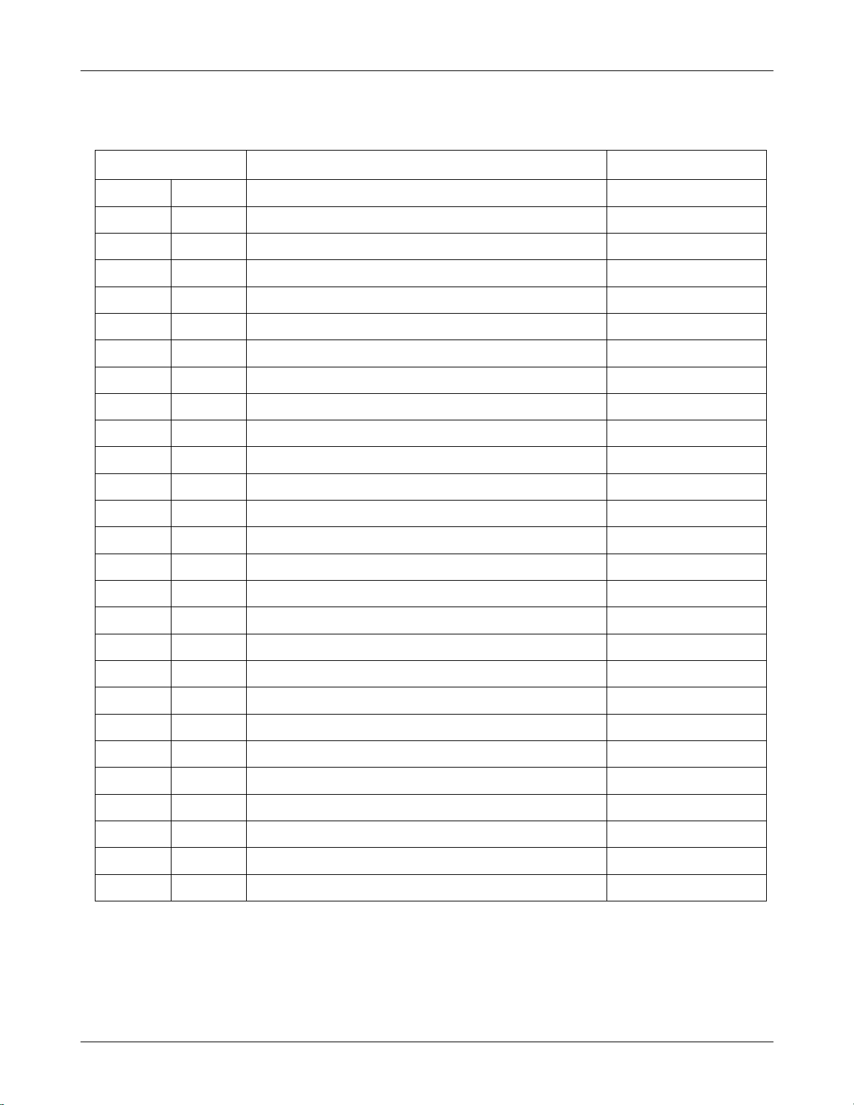
4. Electrical Parts List
Design LOC Description SEC CODE STATUS
BAT30 BATTERY-LI(2ND) 4302-001157 SA
C100 C-CER,CHIP 2203-005482 SA
C101 C-CER,CHIP 2203-005057 SA
C102 C-CER,CHIP 2203-005057 SA
C103 C-CER,CHIP 2203-005482 SA
C104 C-CER,CHIP 2203-000995 SA
C105 C-CER,CHIP 2203-005138 SA
C106 C-CER,CHIP 2203-000359 SA
C107 C-CER,CHIP 2203-000836 SA
C108 C-CER,CHIP 2203-005482 SA
C109 C-CER,CHIP 2203-000812 SA
C110 C-CER,CHIP 2203-001101 SA
C111 C-CER,CHIP 2203-000854 SA
C112 C-CER,CHIP 2203-000812 SA
C113 C-CER,CHIP 2203-005057 SA
C114 C-CER,CHIP 2203-005482 SA
C115 C-CER,CHIP 2203-000812 SA
C116 C-CER,CHIP 2203-000854 SA
C117 C-CER,CHIP 2203-000812 SA
C118 C-CER,CHIP 2203-005496 SA
C119 C-CER,CHIP 2203-000438 SA
C120 C-CER,CHIP 2203-000438 SA
C121 C-CER,CHIP 2203-000278 SA
C122 C-CER,CHIP 2203-005496 SA
C123 C-CER,CHIP 2203-000233 SA
C124 C-CER,CHIP 2203-000278 SA
C125 C-CER,CHIP 2203-006053 SA
C126 C-CER,CHIP 2203-000254 SA
C127 C-CER,CHIP 2203-005482 SA
C128 C-CER,CHIP 2203-005057 SA
C129 C-CER,CHIP 2203-005057 SA
C130 C-CER,CHIP 2203-005482 SA
C131 C-CER,CHIP 2203-000233 SA
C132 C-CER,CHIP 2203-001153 SA
C133 C-CER,CHIP 2203-000604 SA
C134 C-CER,CHIP 2203-000854 SA
C135 C-CER,CHIP 2203-000278 SA
C136 C-CER,CHIP 2203-000585 SA
C137 C-CER,CHIP 2203-000585 SA
C138 C-CER,CHIP 2203-000585 SA
C139 C-CER,CHIP 2203-000585 SA
C141 C-TA,CHIP 2404-001239 SA
C142 C-CER,CHIP 2203-000254 SA
C144 C-CER,CHIP 2203-000812 SA
C145 C-CER,CHIP 2203-000233 SA
C146 C-CER,CHIP 2203-000233 SA
C147 C-CER,CHIP 2203-001383 SA
C148 C-CER,CHIP 2203-000311 SA
C149 C-CER,CHIP 2203-000585 SA
C150 C-CER,CHIP 2203-002443 SA
4-1
SAMSUNG Proprietary-Contents may change without notice
This Document can not be used without Samsung's authorization
 Loading...