

Samsung SGH-E330 Circuit Descriptions
2. SGH-E330 Circuit Description
1. SGH-
E330
RF Circuit Description
1) RX PART
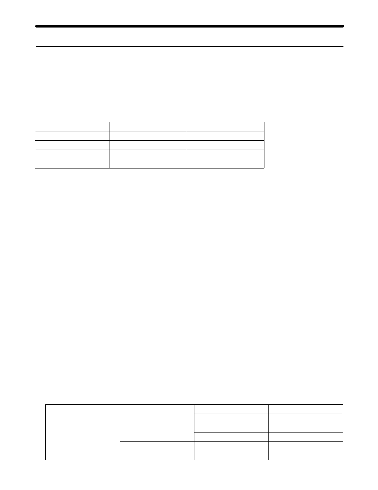
1. ASM(U103)→Switching Tx, Rx path for GSM900, DCS1800 by logic controlling.
2. ASM Control Logic (U103)
GSM Tx Mode H L
DCS Tx Mode L H
GSM Rx Mode L L
DCS Rx Mode L L
3. FILTER
To convert Electromagnetic Field Wave to Acoustic Wave and then pass the specific frequency band.
- GSM FILTER (F100)→For filtering the frequency band between 925 and 960 MHz
- DCS FILTER (F101)→For filtering the frequency band between 1805 and 1880 MHz.
4. VC-TCXO (OSC100)
This module generates the 26MHz reference clock to drive the logic and RF. After additional process, the reference clock
applies to the U100 Rx IQ demodulator and Tx IQ modulator. And then, the oscillator is controlled by serial data to
select channel and use fast lock mode for GPRS high class operation.
→
Truth Table
VC1 VC2
5. Transceiver (U100)
The receiver front-end which amplifies the GSM, DCS aerial signal, converts the chosen channel down to a low IF signal
of 100 kHz. The first stages are symmetrical low noise amplifiers (LNAs). They are matched to 50 ohm. The LNAs are
followed by an IQ down mixer. It consists of two mixers in parallel but driven by quadrature out of phase LO signals.
The In phase (I) and Quadrature phase (Q) IF signals are low pass filtered to provide protection from high frequency
offset interferes. The low IF I and Q signals are then fed into the channel filter. The front-end low IF I and Q outputs
enter the integrated bandpass channel filter with provision for five 8 dB gain steps in front of the filter.
2) TX PART
Baseband IQ signal fed into offset PLL, this function is included inside of U100 chip. OSC101 chip generates modulator
signal which power level is about 6.5dBm and fed into Power Amplifier(U102). The PA output power and power ramping
are well controlled by Auto Power Control circuit. We use offset PLL below table.
GSM -35dBc
DCS -35dBc
GSM -66dBc
DCS -65dBc
GSM -75dBc
DCS -68dBc
Modulation Spectrum
200kHz offset
30 kHz bandwidth
400kHz offset
30 kHz bandwidth
600kHz ~ 1.8MHz offset
30 kHz bandwidth
2-1
SAMSUNG Proprietary-Contents may change without notice
This Document can not be used without Samsung's authorization

Circuit Description
2. Baseband Circuit description of SGH-E330
1. PCF50601
1.1. Power Management
Ten low-dropout regulators designed specifically for GSM applications power the terminal and help ensure optimal system
performance and long battery life. A programmable boost converter provides support for 1.8V, 3.0V, and 5.0V SIMs,
while a self-resetting, electronically fused switch supplies power to external accessories. Ancillary support functions, such
as RTC module and High Voltage Charge pump, Clock generator, aid in reducing both board area and sy stem complexity.
I2C BUS serial interface provides access to control and configuration registers. This interface gives a microprocessor full
control of the PCF50601 and enables system designers to maximize both standby and talk times.
Supervisory functions. including a reset generator, an input voltage monitor, and a temperature sensor, support reliable
system design. These functions work together to ensure proper system behavior during start-up or in the event of a fault
condition(low microprocessor voltage, insufficient battery energy, or excessive die temperature).
Backlight Brightness Modulator
1.2.
The Backlight Brightness Modulator (BBM) contains a programmable Pulse-width
to modulate the intensity of a series of LED’s or to control a DC/DC converter that drives LCD backlight.
But, this phone (SGH-E330) is use UFB LCD. UFB LCD controls backlight brightness by contrast setting.
So "BL_VDD" voltage is always high value when phone is in active mode. When phone is in dimming mode "BL_VDD"
goes to about 10% duty PWM.
modulator (PWM) and FET
Clock Generato
1.3.
The Clock Generator (CG) generates all clocks for internal and external usage. The 32768 Hz crystal
oscillator provides an accurate low clock frequency for the PCF50601 and other circuitry.
r
2. LCD Connector
LCD is consisted of main LCD(color 65K UFB LCD) and sub LCD(color 65K UFB LCD).
Chip select signals LCD_MAIN_CS and LCD_SUB_CS, can enable Each LCD. BACKLIGHT signal enables white LED
of main LCD. "RESET_2V8" signal initiates the reset process of the LCD.
16-bit data lines(LD(0)~LD(15)) transfers data and commands to LCD through bypass capacitor. Data and commands use
"RS" signal. If this signal is high, inputs to LCD are commands. If it is low, inputs to LCD are data.
The signal which informs the state of LCD is whether input or output, is required. But in this system, there is no input
state from LCD. So only "L_WR" signal is used to indicate write data or command to LCD. Power signals for LCD are
"VBAT and "VDD2".
"M_SCL", "M_SCA", "PCLK", "FVALID", "LVALID" and "STANDBY" signals are all related to camera working.
"CAMERA_FLASH_SUPPLY" is voltage supply to flash led , and "SVC_LED" is signal for service led when the signal
is low led is on and vice versa. "SPK_P" and "SPK_N" are used for audio speaker containing voice or melody. And
"VDD_VIB" from PCF50601 enables the motor.
3. Key
This is consisted of key interface pins among OM6359, KBIO(0:7). These signals compose the matrix. Result of matrix
informs the key status to key interface in the OM6359. Power on/off key is separated from the matrix. So power on/off
2-2
SAMSUNG Proprietary-Contents may change without notice
This Document can not be used without Samsung's authorization
 Loading...