

Samsung SGH-E2120, GT-E2120 TSHOO

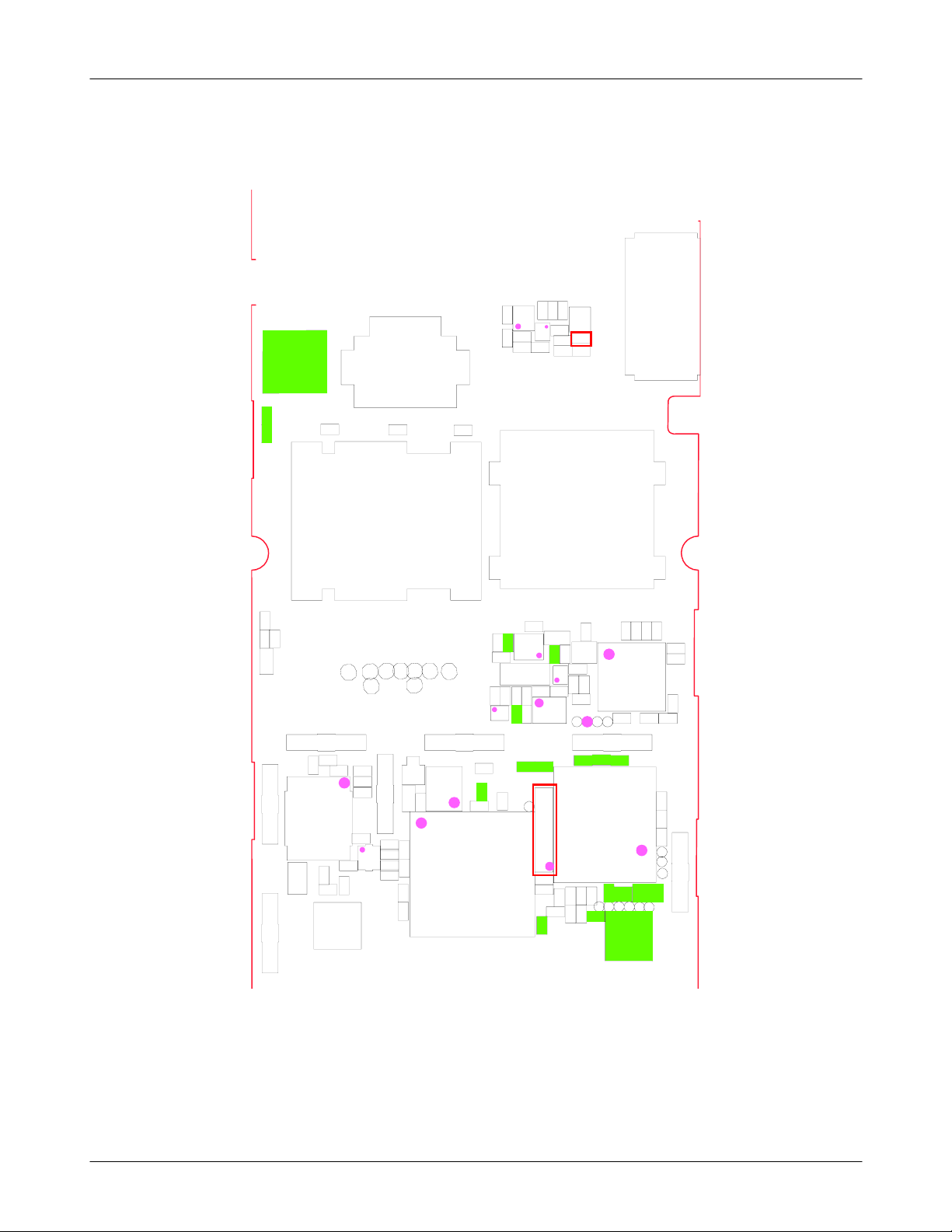
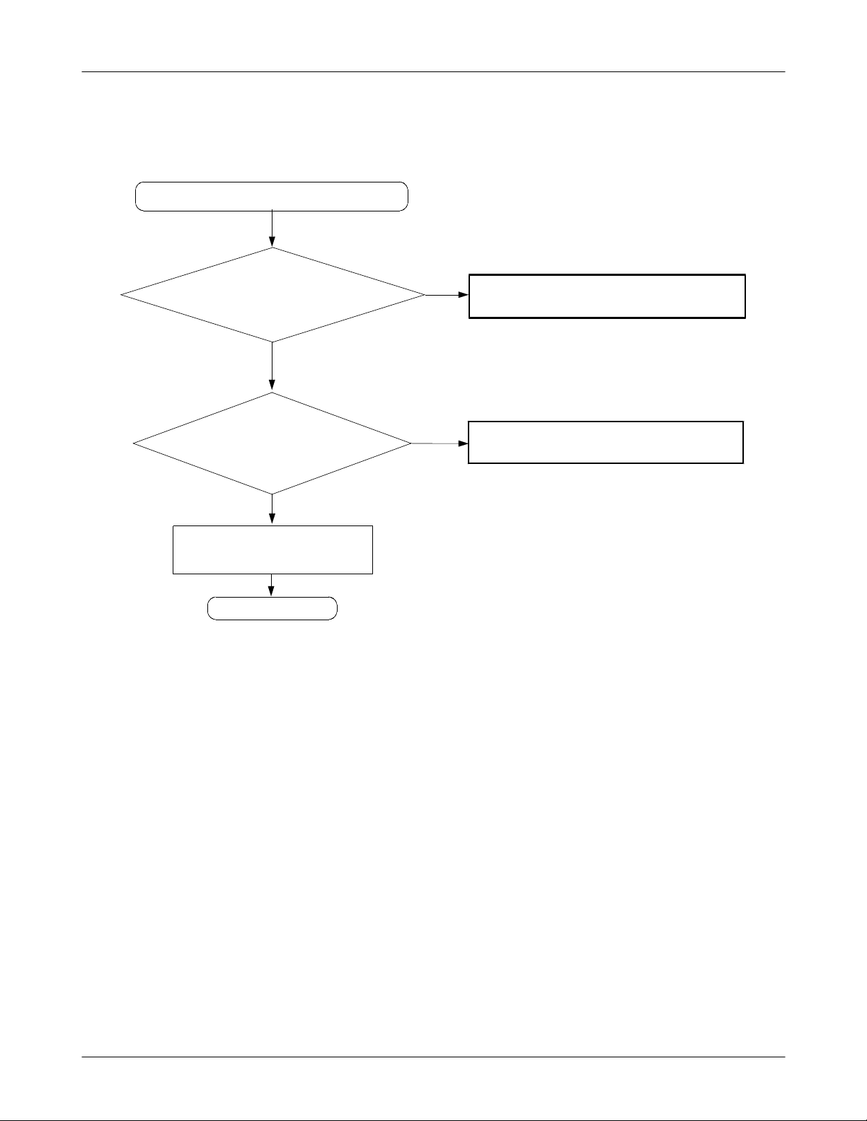
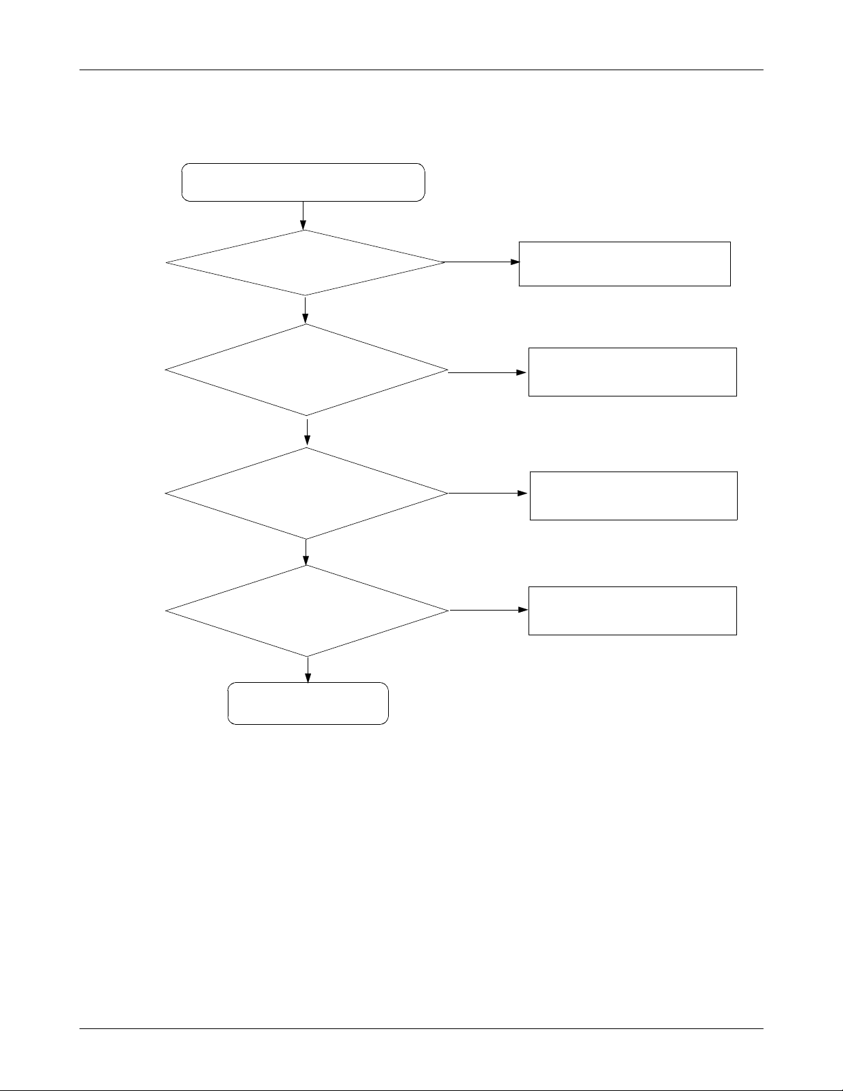
9. Flow Chart of Troubleshooting
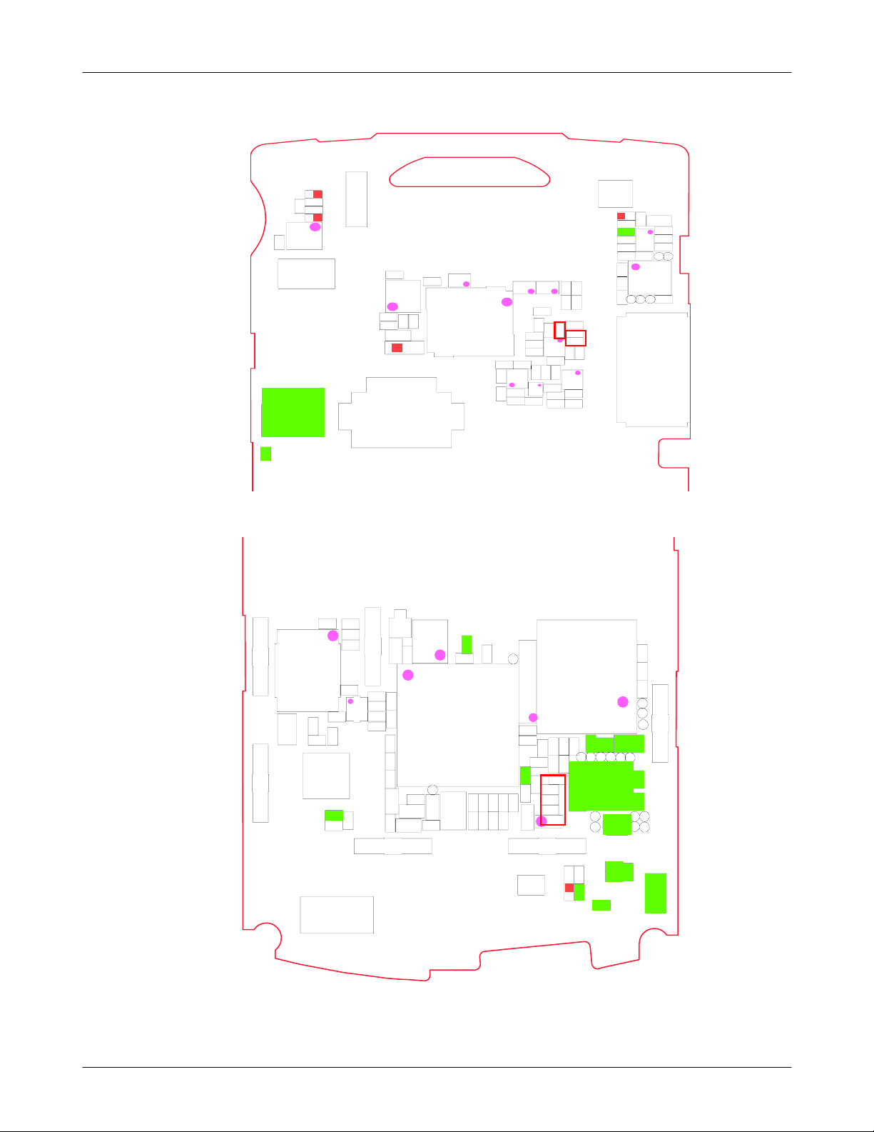
Power On
9-1.
OWER ON' does not work
'P
Yes
Check battery voltage
is higher than
Check VPERM_3.0V,
VANA_2.85V, VRF_2.85V,
VSIM_3.0V, VMEM_1.8V,
VGPIO_2.8V of UCP201
Check the pin1of
OSC201 produces clock
signal
Check the L118
concerning about Jig
Power on
3.3V
OK
OK
OK
Not OK
NotOK
Not OK
Not OK
Change battery
Check the UCP201
older OSC201 again
S
older L118 again
S
OK
No
Is Power On working?
Yes
END
Repeat sequence
9-1
SAMSUNG Proprietary-Contents may change without notice
This Document can not be used without Samsung's authorization
Flow Chart of Troubleshooting
UCP201
PCM_CLK
PCM_DO
PCM_SYNC
PMU_VIO
PMU_VANA
PMU_VMEM
PMU_VPERM
PMU_VRF
PMU_VSIM
POK_OUT
PWM_OUT0
PWM_OUT1
PWM_OUT2
UART0_RD
UART0_TD
UART1_RD
UART1_TD
UART1_CTS
UART1_RTS
XTAL_26M_1
XTAL_26M_2
XTAL_32K_1
XTAL_32K_2
XTAL_SHLD
XTAL_SHLD
XTAL_SHLD
XTAL_SHLD
XTAL_SHLD
XTAL_SHLD
SIM_CLK
SIM_DATA
SIM_RST
PCM_DI
POK_IN
RFID_N
RFID_P
RFIL_N
RFIL_P
RFIP_N
RFIP_P
J19
H15
H16
J18
W15
W14
V15
L201
W12
W13
V14
T8
V8
T7
T5
T6
W8
ICHGN
W9
ICHGP
E1
D1
G1
F1
C1
B1
A1
RFOH
A2
RFOL
L18
K18
W5
V5
V7
W6
A7
A6
L19
K19
B8
A8
B6
A5
B7
B5
H19
H18
G16
DCL
DU
DD
FSC
VGPIO_2.8V
VANA_2.85V
VMEM_1.8V
VPERM_3.0V
VRF_2.85V
VSIM_3.0V
ONKEY_2
ONKEY_1
ICHGN
ICHGP
DCSRX_N
DCSRX_P
EGSMRX_N
EGSMRX_P
DCS_TX
EGSM_TX
UART0_TD
UART0_RD
UART1_RD
UART1_TD
OSC200
2
OSC201
1
3
2
SIM_CLK
SIM_DATA
SIM_RST
3
4
1
IFC100
HY20-AB0310
1
1
2
2
3
3
4
4
5
5
6
6
7
7
8
8
9
9
10
10
11
11
12
12
13
13
14
14
15
15
16
16
17
17
18
18
19
19
20
20
21
NC
22
NC
23
NC
24
NC
25
NC
26
NC
27
NC
VBAT
VCHG_5V
EAR_SW_REF
C133
C136
C138
L111
L113
R122
L115
L116
R123
L117
JIG_ON_IF
L118
R125
R126
R129
TA_DETECT
6
5
4
2
ZD104
1005
R120
6
5
3
1
R_ANT
EAR_N
VCM_OUT
EAR_P
EAR_SW
AUX_DET
UART0_TD
UART0_RD
JIG_ON
C147
C150
C149
4
3
1
2
ZD105
C148
VDD_3.3V
R124
0
0
1
Q
R117
C134
C132
EAR_MIC_P
C135
C137
R119
2
S
G
1
3
D
C139
USB_EN
USB_DP
USB_DM
EAR_MIC_N
R128
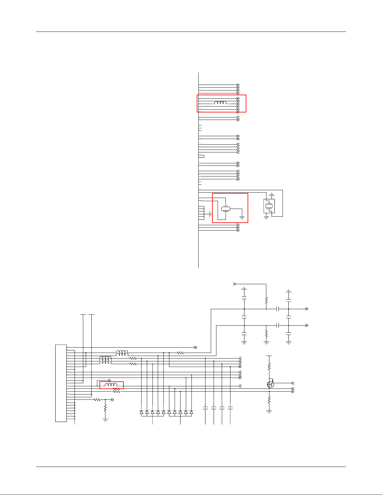
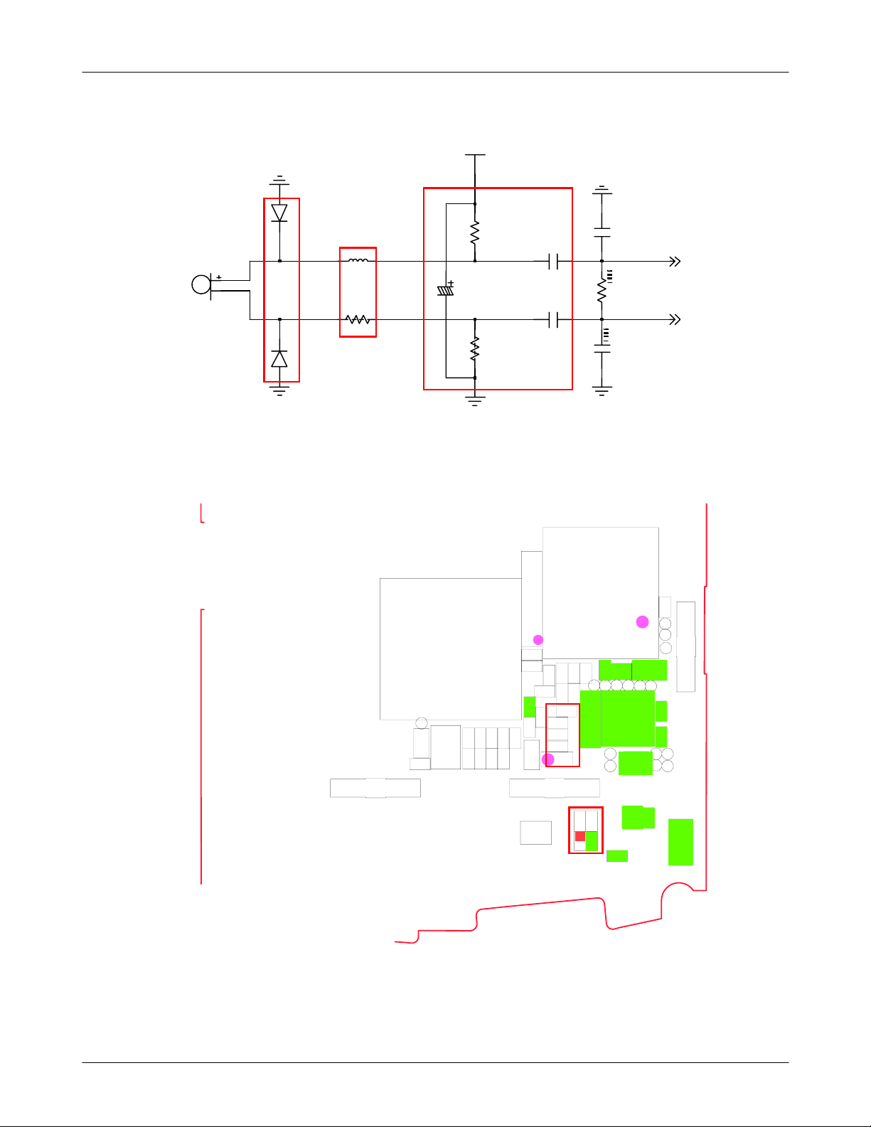
9-2
SAMSUNG Proprietary-Contents may change without notice
This Document can not be used without Samsung's authorization
BAT200
R
2
0
4
C
2
2
3
Flow Chart of Troubleshooting
0
C
R
1
1
C
5
2
3
0
3
1
6
U304
R
2
0
C317
1
C229
R136
1
0
5
D
Z
1
0
5
U
R126
L118
R125
R127
R129
BTC201
R133
R134
R135
0
1
C
F
I
SIM201
C
2
3
3
C
R
2
2
3
1
2
3
C
2
3
4
SC101
C
R113
1
3
0
C131
S
P
C
1
0
A
0
M
1
0
0
C
C
1
1
1
6
1
9
L112
TP_GND
C123
C
1
0
6
T
T
T
P
P
P
_
T
_
_
I
D
_
T
P
T
K
C
T
_
R
P
T
R
T
T
M
D
O
S
TP_RSTON
R116
R114
3
0
R115
1
C
S
C120
L
1
C122
0
F
2
1
C117
0
0
L
1
0
C127
6
C125
C
2
0
4
R
2
1
2
D200
C
2
0
8
I
P
_
2
O
.
8
V
_
G
T
P
V
S
T
_
N
T
P
_
T
C
K
0
0
2
C
C
S
2
0
1
O
UCP201
C
C
2
2
3
3
5
6
R211
R214
C
C
C
3
3
3
0
1
0
8
5
9
U
R
3
3
0
2
2
3
1
0
8
C
S
R203
C
2
2
2
C
2
1
7
C214
SD300
C
R
R
R
3
3
3
3
0
0
0
1
6
7
9
0
R308
R306
U301
C
3
0
T
T
P
P
R311
3
3
0
0
1
6
1
0
4
C
S
C224
C221
1
0
2
E
M
U
C
R
1
1
1
0
1
9
S
O
I
I_
T
N
P
S
C
D
_
I
I_
P
P
S
S
C128
0
L300
C304
C
2
0
5
R
2
0
0
C
2
0
6
3
0
4
P
T
2
0
1
P
T
S
C
C
H
G
1
_
0
S
6
W
C
C
C
1
1
1
1
1
0
1
0
4
7
5
1
U
K
1
0
0
L
C
SPI_DI
_
I
P
S
C218
R207
TH200
R
1
2
8
C237
Q
C
C
1
3
2
0
0
3
0
2
8
R124
U300
C
C
3
3
0
0
1
3
C313
U
C307
3
0
5
3
0
0
P
T
U310
C219
O
S
C
2
0
1
C
C
C
1
1
1
3
3
3
5
7
9
R
C
1
1
C132
1
3
7
4
R215
0
0
2
U
R
3
R320
2
1
R
3
2
2
C220
T
P
2
0
0
9-3
SAMSUNG Proprietary-Contents may change without notice
This Document can not be used without Samsung's authorization
Flow Chart of Troubleshooting
9-2. S
IM Part
Insert SIM" is displayed on the LCD
"
VSIM_3.0V at the pin#1
SIM
200 = "
Is there any signal pin
#2,3,4
Yes
of SIM
Yes
H"?
201?
No
No
Check the SIM Power
Check UCP201
Check the SIM Card
END
9-4
SAMSUNG Proprietary-Contents may change without notice
This Document can not be used without Samsung's authorization
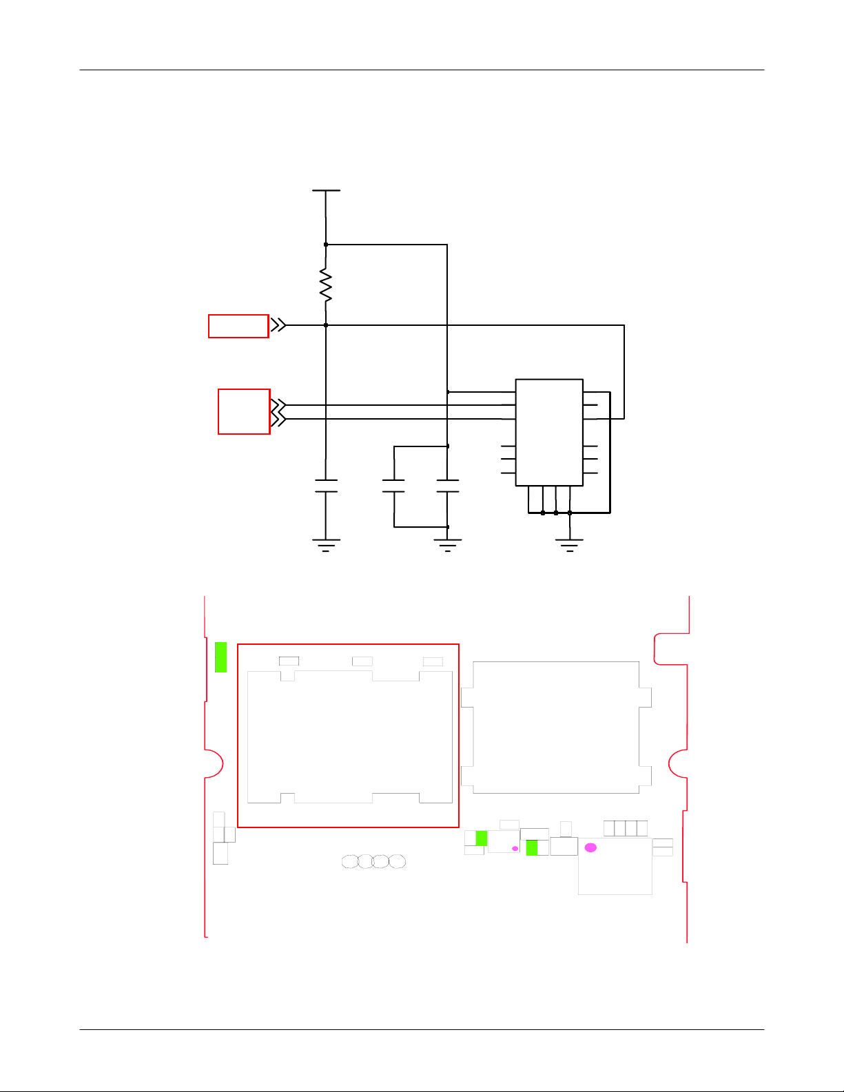
SIM_DATA
Flow Chart of Troubleshooting
VSIM_3.0V
R213
SIM201
SIM_RST
SIM_CLK
R
2
0
4
C
2
2
3
C233
C234
C232
1
2
3
7
7
88
99
G
11 11
G
6
5
4
1212
1010
1314GG1516
R133
SIM201
R134
R135
SD300
C
2
3
3
C
R
2
2
3
1
2
3
C
2
3
4
T
T
P
P
_
T
_
R
T
S
M
T
_
S
N
R215
C
C
2
2
3
3
6
5
R211
C237
0
0
C
C
2
3
2
0
3
U
2
8
9-5
SAMSUNG Proprietary-Contents may change without notice
This Document can not be used without Samsung's authorization
C
R
R
R
1
2
8
Q
1
0
0
R
3
3
3
3
0
0
0
1
7
9
6
0
R308
R306
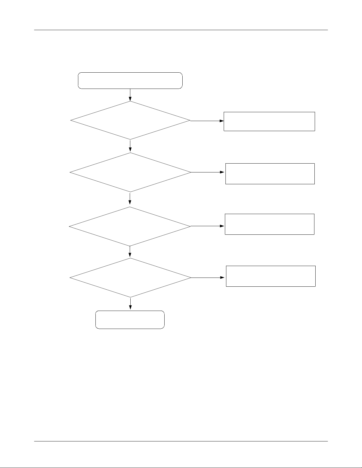
Flow Chart of Troubleshooting
Microphone Part-Phone MIC
9-3.
Phone MIC does not work
Yes
Check the connection
of MIC
OK
Check thecomponents
which are connected to
MIC_BIAS
OK
Check the circuit
of MIC PART
OK
Is Phone MIC working?
Not OK
Not OK
Not OK
No
older MIC again
S
Solder R118, R132, C141, C145 and
older L108, R131, ZD100 and ZD103
S
C142 again
again.
Replace MIC
Yes
END
9-6
SAMSUNG Proprietary-Contents may change without notice
This Document can not be used without Samsung's authorization
MIC_BIAS
Flow Chart of Troubleshooting
MIC100
0
0
1
D
Z
3
0
1
D
Z
L108
R131
0ohm
C142
R118
R132
C141
C145
C140
MIC_P
R130
MIC_N
C146
MAIN_MIC
C
2
0
5
C
2
0
6
4
3
0
P
T
0
1
2
P
T
S
C
C
H
1
G
_
0
S
6
W
C
C
C
1
1
1
1
1
0
1
0
5
7
4
1
U
K
1
0
0
L
C
SPI_DI
_
I
P
S
C
1
1
1
0
3
U
2
C
1
0
8
DD100DU100
0
0
1
T
F101
S
DCL100
R
_
T
B
C200
TP305
C
2
0
9
UCP201
L
2
0
2
1
O
S
C
2
0
1
R207
C
TH200
C
1
1
3
3
5
9
C
1
C132
3
4
C
1
4
6
R
R132
1
3
0
C
1
C145
4
0
R
C
C
R
C
2
2
2
2
2
0
0
1
1
9
7
2
1
C
C
C
L
2
2
2
2
0
0
1
1
1
0
2
3
C141
1
0
C
R118
2
2
8
C142
1
0
7
C
S
0
2
E
M
U
C
R
C
1
1
1
1
0
1
3
9
7
S
O
I
P
S
_
I
T
N
C
C128
C118
C109
C113
C111
D
I_
I_
P
P
S
S
U
M
P
_
N
O
FSC100
R
1
1
7
R
L
1
1
0
3
8
1
Z
Z
D
MIC100
D
1
1
0
0
3
0
C151
9-7
SAMSUNG Proprietary-Contents may change without notice
This Document can not be used without Samsung's authorization
L107
L120
C
1
5
2
A
N
T
1
0
2
Flow Chart of Troubleshooting
Earphone MIC does not work
Microphone Part-Earphone MIC
9-4.
Yes
Check the connection
of IFC100
OK
Check MIC_BIAS.
When UCP201 operates
(
and call is connected
OK
Check the circuit
of EAR MIC
OK
Is Earphone MIC working?
)
Not OK
Not OK
Not OK
No
older pin3of IFC100 again
S
Solder R118, R132, C141, C145 and
older L111, L113 and R120 again
S
C142 again
Repeat the sequence
Yes
END
9-8
SAMSUNG Proprietary-Contents may change without notice
This Document can not be used without Samsung's authorization
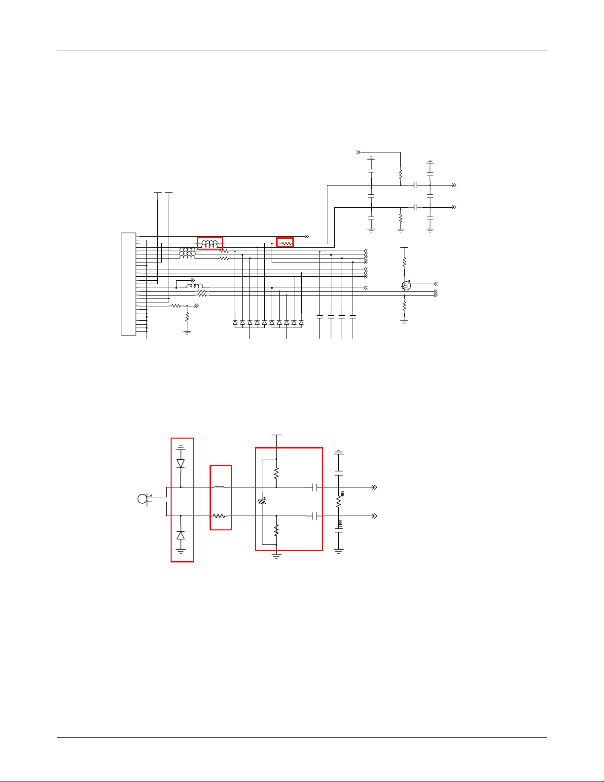
IFC100
HY20-AB0310
1
1
2
2
3
3
4
4
5
5
6
6
7
7
8
8
9
9
10
10
11
11
12
12
13
13
14
14
15
15
16
16
17
17
18
18
19
19
20
20
21
NC
22
NC
23
NC
24
NC
25
NC
26
NC
27
NC
Flow Chart of Troubleshooting
EAR_SW_REF
C133
R117
VCHG_5V
VBAT
L111
L113
L115
R122
L116
L117
R123
JIG_ON_IF
L118
R125
R126
TA_DETECT
1005
R129
6
5
R120
6
4
3
1
2
ZD104
R_ANT
C147
C150
5
4
3
1
2
ZD105
C149
C136
C138
R119
VDD_3.3V
EAR_N
VCM_OUT
EAR_P
R124
EAR_SW
AUX_DET
UART0_TD
UART0_RD
0
0
1
Q
JIG_ON
C148
3
D
C132
C134
C137
2
S
G
1
R128
EAR_MIC_P
C135
EAR_MIC_N
C139
USB_EN
USB_DP
USB_DM
MIC100
0
0
1
L108
D
Z
R131
0ohm
3
0
1
D
Z
MAIN_MIC
MIC_BIAS
C142
R118
R132
C141
C145
C140
MIC_P
R130
MIC_N
C146
9-9
SAMSUNG Proprietary-Contents may change without notice
This Document can not be used without Samsung's authorization
Flow Chart of Troubleshooting
R
3
2
4
BAT200
R
2
0
4
C
1
4
3
L302
S
P
E
A
ZD101
L110
L109
ZD102
3
0
7
K
E
R
_
P
A
D
U
R325
3
F
0
3
C305
3
3
F
F
0
0
1
2
U303
R
R
C310
3
3
1
1
2
3
C230
C231
1
0
3
C
D
H
D201
C312
C
1
3
R
C
3
1
1
2
3
0
6
C138
1
0
4
C147
C149
L301
C
3
1
6
R
2
0
1
L116
C311
R
C
L
1
1
1
1
2
5
7
3
0
U304
1
0
5
U
R126
C317
R125
C229
R136
BTC201
ANT100
C
1
ZD106
0
2
L100
L119
C101
C104
U
1
0
C100
R107
0
R100
C105
1
P
T
0
1
0
1
P
T
C153
L
1
0
4
C
1
C
C
1
1
2
2
4
6
R
R
1
1
1
1
2
1
C148
L111
L113
D
Z
R
1
2
2
1
0
5
L118
R127R129
2
1
L
1
0
5
L
1
1
5
D
Z
0
R101
U102
1
T
P
0
2
1
P
T
0
1
3
P
T
0
4
C129
0
0
1
C
IF
R114
S
C
1
0
0
R115
P
A
M
1
0
0
C120
C
1
1
6
C
1
0
6
L112
RFS100
R106
L114
C123
C
1
0
3
C
1
1
9
5
0
1
C
S
D200
3
C
0
1
2
C
0
S
8
L
1
C122
0
F
2
1
C117
0
0
L
1
0
C127
6
C125
C
2
0
4
R
2
1
2
R
2
0
6
C
2
1
6
R
2
0
2
SC102
C215
C
2
0
1
L200
0
0
C
2
2
2
C
2
C
S
O
UCP201
TP305
C
C203
2
0
9
C200
2
1
T
P
7
2
C214
L
2
0
2
0
0
O
S
C
2
0
1
R207
TH200
C
1
3
9
C132
C
1
4
6
R
1
3
0
C
1
C145
4
C
2
0
7
C
2
1
0
0
R
C
C
R
2
2
2
2
0
1
1
9
2
1
C
C
L
2
2
2
0
0
1
1
2
3
C141
1
0
C
R118
2
2
8
C142
1
0
7
MIC100
1
0
2
E
M
U
C
R
C
C
1
1
1
1
1
0
1
3
3
9
5
7
S
I
P
S
_
I
T
N
C
_
R
I
C
P
1
S
1
1
3
7
4
C128
C118
R132
C109
C113
C111
U
M
P
_
N
O
FSC100
C
S
R
L
1
1
0
3
8
1
Z
Z
D
D
1
1
0
0
3
0
C151
C
2
0
5
R
2
0
0
C
2
0
6
3
0
4
P
T
0
1
2
P
T
S
C
C
H
1
G
_
0
S
6
W
C
C
C
1
1
1
1
0
1
1
0
7
4
5
1
U
O
K
0
1
0
L
D
C
_
SPI_DI
I
_
I
P
P
S
S
C
1
1
1
0
3
U
2
C
1
0
8
DD100DU100
0
0
1
T
F101
S
DCL100
R
_
T
B
C
L107
1
5
2
L120
A
N
T
1
0
2
ANT101
9-10
SAMSUNG Proprietary-Contents may change without notice
This Document can not be used without Samsung's authorization
 Loading...