

Page 1
SF150T 5-1
5. Circuit Description
5-1 General
The main circuit board controls the machine, and consists of Super Fax Chip (KS16118), External memory,
CODEC circuit with modem-TX and RX signal path and some parts of the Line Interface Unit, Digital TAD
circuit with DSP amd DRAM, witch controls the system.
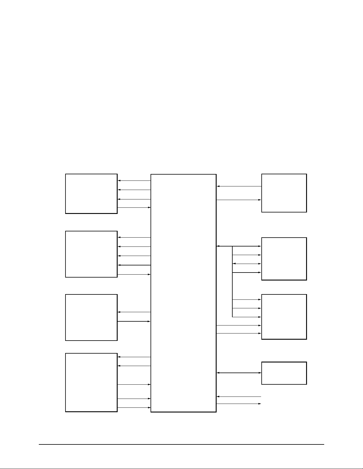
5-2 System Control Section
This circuit consists of the EP-ROM and SRAM, external Real Time Clock crystal, RTC and memory back-up
circuitry, and the Super Fax Chip (KS16118).
The KS16118 Super Fax Chip is an integrated 9600 bps modem, image processor, 8-bit MPU, peripheral
controller, and analog front end circuit on a single-chip.
Peripheral functions inculde 2-channel SI0, 3-channel DMA, 6-bit Half flash A/D converter, scanner and
video processor units, TPH interface, CODEC unit, and tone generator.
Modem is a 9600 bps, half duplex monolithic device incorporating digital filters, a Samsung SSP1600 digital
signal processor and CPU-Interface logic.
Figure 5-1: KS16118 External Memory Map
1FFFH
0100H
00FFH
0000H
0000H
FFFFH
FF80H
FF7FH
FF00H
FEFFH
/DMS
(SRAM)
Peripheral
PCS0
DSP /CS
PCS1
Interrupt
Vectors
/PMS
(EP-ROM)
[ Program Memory ]
[ Data Memory ]
5-2-1 Memory Map
The external memory of the CPU is devided into, 1 byte(FF00H) DSP chip select, 32kbyte SRAM (0000H
through 7FFFH) and 128kbyte EP-ROM (0100H through 1FFFH).
Page 2
Circuit Description
5-2 SF150T
Figure 5-2: XFC Hardware Interface Signals
5-2-2 lExternal Chip Control
KS16118 internal logic generates chip select signals for both memory chips and peripherals.
To support external access, from one to three wait cycles can be inserted under program control during
external access.
A chip select signal line goes active (low) whenever its corresponding device is accessed over the external
interface. The peripheral addresses are located in data memory space.
/DMS : SRAM chip select active (low)
/PMS : EP-ROM chip select active (low)
/PCSn : Peripheral chip select active (low)
D0 - D7 : 8 bit data bus
A0 - A15 : address bus
5-2-3 System Clock
The 12 MHz internal system clock frequency is generated by dividing the 24 MHz clock.
OPERATING
PANEL
PRINTER DATA
CONTROL AND
SENSORS
MOTOR
DRIVER
(MOTOR)
SCANNER
CONTROL
AND
PROCESSING
RTC
CRYSTAL
DATA
MEMORY
PROGRAM
MEMORY
GENERAL
PURPOSE I/ 0
OP00-OP06
LED_CTL
LCD_EN
OPI0-OPI3
STB 0-3
PDAT
PCLK
PLAT
THADI
SM0-SM3
MODE
SI
CLK1
Vin
+Vref
-Vref
XIN
XOUT
/DMS
/RD /WR
D0~D7
A0~A14
/RD
D0~D7
A0~A15
A16
/PMS
RESTOUT
/RESET
KS16118
Page 3
Circuit Description
SF150T 5-3
Figure 5-4: Printer Timing
5-2-4 Real Time Clock (RTC)
This circuit receives clock pulses from an external
32.768 kHz crystal, which it divides into hours,
minutes, seconds, year, month, and day.
A battery maintains operation when power is off.
KS16118 can up-track 100 years, begining with
1992.
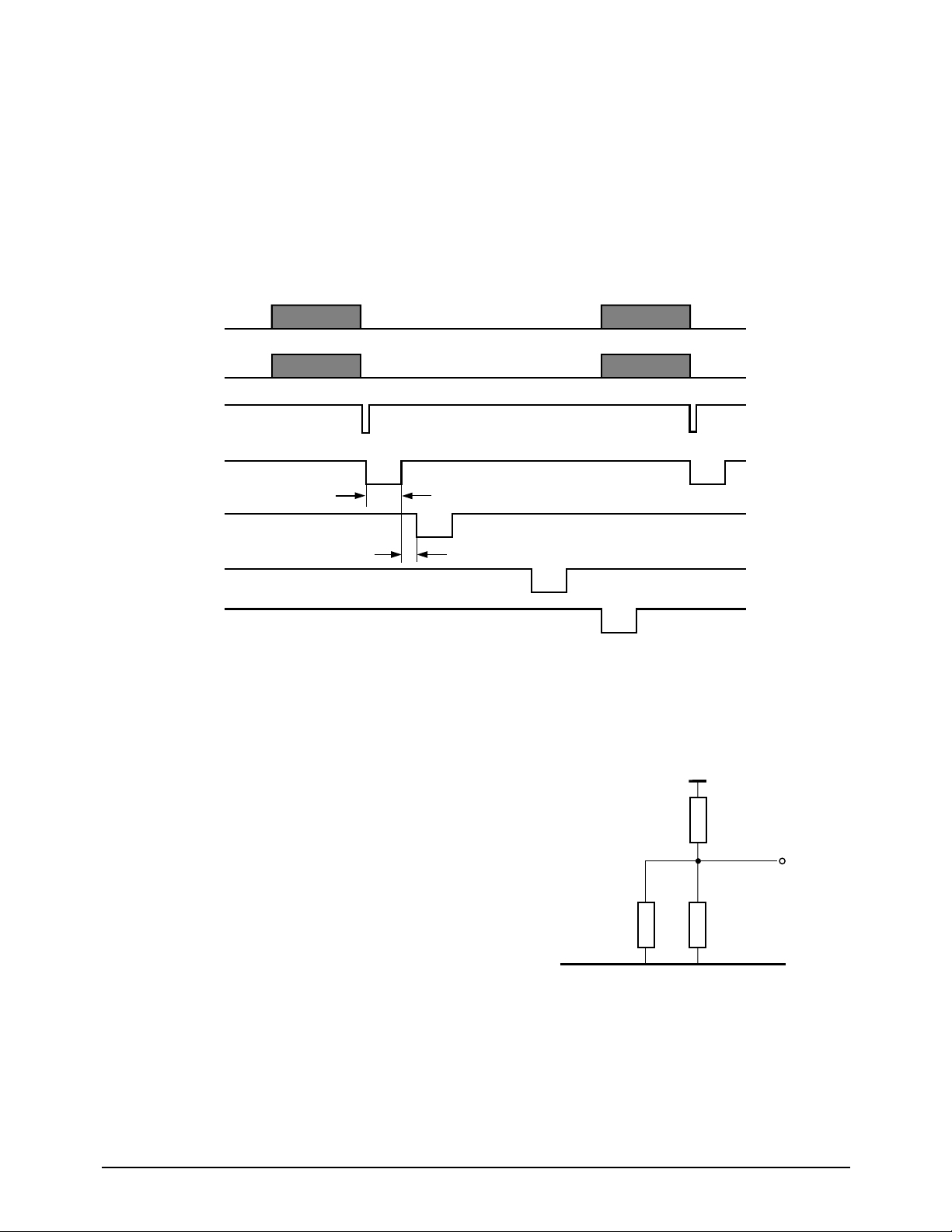
5-2-5 Print Control
The PCLK and PDATA signals synchronize serial
print data to the TPH.
PLAT latches TPH serial print data to the TPH
from a shift register through PDATA.
STB0 - STB3 enable TPH printing in four steps.
This system has a 10ms/line printing format and
sets STB High/Low enable status
according to the STBPOL signal.
PDATA
PCLK
PLAT
STB0
STB1
STB2
STBWID
[0:11]
STB0FF
[0:11]
STB3
Figure 5-6: THD Connection Circuit
GND5
THD1
+5V
R5
R4
Rth
(T)
TPH
Thermistor
5-2-6. A/D Converter (Scanner & TPH
Temperature)
Using a half-flash conversion technique, the 6-bit
A/D converter supports a 0.8µs peak conversion
time and dissipates only 7mA, maximum.
The half-flash unit uses 16 comparators, a most
significant 3-bit ADC, and a least significant 3-bit
ADC.
If the analog input voltage is greater than +Vref,
the A/D conversion result is 3FH.
If the analog input voltage is less than -Vref, the
A/D conversion result is 00H.
A/D conversion register, ADCON (19H), is used
to select an internal or external source for the A/D
converter, to enable or disable the converter, and
to select the operating mode (H: ADin 1 (Scanner),
L: ADin 0 (TPH)).
Page 4

Circuit Description
5-4 SF150T
5-2-7 Operation Panel Control
Communication
The Operation Panel is controlled by the Port 1,
Port2, and Port 5 registers.
Port 1 (E2H) is a 4-bit general output port for LCD
display data.
This port can be configured for normal data (P1.4P1.7) or alternately as internal MODEM V.24
interface output signals (P1.0-P1.3).
Port 2 (E4H) is an 8-bit port with both input and
I/O pins.
P2.0-P2.3 are input ports for OPE key scan data,
and P2.6-P2.7 are not used for SF150T.
Port 5 (EAH) is an 8-bit port with both output and
I/O pins.
P5.0 and P5.4 are used for LED control and LCD
enable.
5-2-8 Image Sensor
The shading wave is formed by scanning the white
roller prior to a document.
The slice level is determined by the shading wave,
and compensates for shading distortion according
to the CIS characteristics.
The wave format from the CIS is converted into a 6
bit digital value in the KS16118 image processor,
and processed in B/W or intermediate mode.
5-2-9 CIS Input Processor
To process the B/W input signal, maximum (+Vref)
and minimum (-Vref) values of the CIS input signal
are adjusted by calibrating KS16118 in the high state
for maximum level, and setting them to earth for
minimum level.
Shading correction uses a multiplier composed of a
9-bit sequential adder for simple H/W Logic.
5-2-10 CIS Driver
The CIS driver clock (CLK1) frequency is 250 kHz.
A 75% low duty cycle lengthens the charging time.
A start signal (SI) is provided every 10 ms to
match the line scanning time.
Actual image signal (VIN) is provided in less than
6.8 ms, based on A4 paper size using the 250 kHz
clock.
Figure 5-10: CIS Driver Clock Timing
250 KHZ (L:DUTY 75%)
SI
CLOCK
SIG
1 LINE
Page 5

Circuit Description
SF150T 5-5
5-2-11 I/O Port Table
High Bank Memory
DSP Inactive
DATA = 1
DATA = 1
Active
Active
Active
Active
-
Active
Active
DSP Reset
DSP High Byte
Normal
Normal
CIS LED On
High
OPE LED On
Normal
Normal
-
Open
No Paper
No Document
Normal
Normal
CODEC Serial Clock
CODEC Serial Data
CODEC Enable
-
Closed
Paper Exist
Document Exist
Incomming Ring
Active DSP Data Transfer
Low Bank Memory
DSP Active
DATA = 0
DATA = 0
Inactive
Inactive
Inactive
Inactive
-
Inactive
Inactive
Normal
DSP Low Byte
Low Battery
DSP Response Mode
Off
Low
OPE LED Off
No Barttery
Circuit Symbol
I/O
Pin No.
Port Name
High Low
A16
/DSP_CS
IRXD
ITXD
MOTOR A
MOTOR /A
MOTOR B
MOTOR /B
/CML2
/CML1
/24VCTL
DSPRST
DSPHL
/LOWBAT
DSPACK
/GLED
-
LEDCTL
/NOBAT
SCLK
SDATS
/SDEN
/HOOK DET2
MODE
P_EMPTY
D_DET
RING_DET
/DSPFLAG
P0.0
P0.1
P2.4
P2.5
P3.0
P3.1
P3.2
P3.3
P3.4
P3.5
P3.6
P4.1
P4.2
P4.4
P4.5
P4.6
P4.7
P5.0
P5.3
P5.5
P5.6
P5.7
P6.1
P6.2
P6.3
P6.4
P6.5
P6.6
O
PCS
I
O
O
O
O
O
O
O
O
O
O
I
O
O
O
O
I
O
O
I
I
I
I
I
I
I
34
35
45
46
49
50
51
52
53
54
55
93
92
90
89
87
88
126
96
137
138
139
59
60
61
62
63
116
Page 6

5-2-12 Motor Controller
This facsimile machine perform sending, receving,
and printing functions utilising a single 24 volt
motor with a 120 ohm winding resistance.
Four drive strobe pulses operate the motor.
5-2-13 Serial communication Signals
The KS16118 have two full-duplex serial
communication port.
One port is used for I-LIU communication on LIU
PBA, and is a standart UART (Universal
Asynchronous Receiver/Transmitter).
Another port, not used, may be configured for
UART or SRT (Synchronous
Receiver/Transmitter) operation.
5-2-14 Reset
To initialize the chipÕs internal logic, the reset
input (/RESET) must be held to 0 Volt for at least
22 CPU clocks. During this time, Vdd must be
greater than 3 Volt.
The watchdog timer can also invoke a system
reset.
When the reset input is released, the reset
condition continues for about 209.7 ms.
While the KS16118 is in this state, 0 Volt is applied
to the /RSTOUT pin.
[ +5V Power Monitoring ]
If 5 volt power to MX93000AFCÕs pin 6 (VPOW)
drops to between 4.6V and 4.4V (typically 4.5V),
power failure is indicated and the output of
MX93000AFCÕs pin 5 (/POWB) will go `lowÕ(GND5).
This causes the KS16118 to become active (low=reset).
The KS16118 reset causes the /REST0 terminal to be
reset.
Circuit Description
5-6 SF150T
Table 5-1: Motor Functions
Motor Function
Swing Gear Control
Document Out
100 pps
100pps
Drive Strobe Pulse
Phase
2
2
Other 100pps
2
Super Fine Mode 100pps
1-2
5-3 Memory
System memory consists of 128 kB EP-ROM and 32 kB SRAM. All of SRAM is backed up.
ROM and SRAM are selected by chip select lines, and data is accessed by the units position of the byte.
ROM has two banks. One Bank is as low bank that address range is 0100H-FFFFH.
Another bank is as high bank 10000H-1FFFFH. ROMÕs bank is selected port 0 (bit 0) of the KS16118.
5V power is applied to SRAM through VB. This model facsimile machine uses a Lithium battery.
A 1 kohm resistor in series with the positive battery terminal is for battery protection.
5-4 CODEC circuit with Modem-TX and RX signal path
This has PCB CODEC which has ablity that converts voice signal to A/D and is able to store is DRAM and convert
to voice signal passing through D/A transmission after scanning from voice digital stored in DRAM by DSP.
This has PRE-PGA(Programmable Gain Amplifier) that is able to amplift selectively among Mic input, remot
signal, rx signal.
This has ALC(Automatic Level Control) circuit has maximum 42dB gain to be convenient for recording using Mic.
This have two comparator having 1.25V reference voltage and two universal opamp.
This has 1 W speaker drive amplifir that is able to drive 8 ohm speaker.
Because MX93000AFCÕs control uses synchronous communication port, that is fast in action is convenient.
Page 7

Circuit Description
SF150T 5-7
5-5-1 DSP
This circuit consists of host interface, memory
interface, CODEC interface.
receives data to the compressed voice data to and
from KS16118.
Memory interface sends and receives data to the
compressed voice data to and from DRAM to play
back and record voice data.
DSP communicates with host KS16118 through host
interface.
5-5-2 Recording Path
The voltage is supplied with MIC as using the
MX93000AFC's Vref Voltage (2.25V), and the voltage
entering into MIC is trasmitted to electric signal and
enters into MX93000AFC's MIC terminal.
Input signal is amplified by MX93000AFC's ALC
until maximum 26dB (Max. 3VP-P) according to
signal size.
The signal enters into PCM CODEC that converts to
D/A and compresses in the DSP Chip and stores in
DRAM.
5-5-3 Play Path
The signal stored in DRAM is decomressed in DSP
and enters into MX93000AFC.
Input signal is converted to D/A again and is
amplified by LIU-DRV amplifier and comes into
LOUT terminal through or comes into terminal
after being attanuated by ATT (Electronic Volume)
or SPK-DRV.
5-5-4 Voice Backup
+5V is supplied for DSP or voice memory through
VBT when power is on.
When power is off, +5V is supplied from the 9V
backup battery.
When supply voltage is "ON", U9(5V Voltage
Regulator) makes 5V Supply Voltage.
The signal is supplied with DSP or DRAM and it
caused that the data is protected.
When supply voltage is "OFF", U9 makes 5V Voltage
as using the 9V Battery.
And then the voltage is used to "backup supply
voltage" in DSP or DRAM.
If the supply voltage were "OFF" as using the full
charged 9V Battery, voice data is usually protected
for twenty hours.
5-5 TAD
TAD circuit consists of a voice coprocessor to record and play voice messages and voice memory.
1) TX CIRCUIT
The output signal coming from internal modem
KS16118 enters MX93000AFC through AUX2
terminal after amplfied by OP AMP U1.
That signal passes through internal switch, is
amplified by LIN-DRV amplfier and is sent to LIU
board through LOUT terminal.
2) RX CIRCUIT
The signal goming into LIU terminal through LIU
board is amplified by MX93000AFC's PRE-PGA,
passes through internal switch and goes into FILT
terminal.
After the singal is diminished by OP AMP U1, it
enters internal modem of KS16118.
Page 8

Circuit Description
5-8 SF150T
5-6-1 FAX section
MODEM/LINE INTERFACE
This is the path for data and control signals.
¥ CML201 relay: switches telephone line between
FAX and telephone circuits.
¥ U201 pin 3 TIT: single-ended input for
transformer T202.
¨ TIT: Transmit Input from Transformer
¥ U201 pin 40 ROT : Output for driving a
transformer T203 with an AC impedance
exceeding 10Kohm.
¨ ROT: Receive Output Transformer
¥ C212: DTMF and CNG detect path to T201
20Kohm winding under idle conditons; and DC
blocking for 20Kohm winding.
¥ AC impedance: the AC impedance of U201 (I-
LIU) is set at 1000ohm by external capacitor
C228 at U201 pin 8 CI (Complex Impedance
input) port. With an external resistor (R244) at
U201 pin 34 ACI port it can be programmed to
600ohm. And U201 pin 35 CS (Current Shunt
control output) port is N-channel open drain
output to control the external high power shunt
transistor for synthesizing AC and DC
impedance.
¥ DC conditions : normal operating mode is from
15mA to 100mA. An operating mode with
reduced performance is from 5mA to 15mA. In
the line hold range from 0mA to 5mA the device
is in a power down mode and the voltage at
U201 pin 37 LI (Line Input) port is reduced to a
maximum of 3.5V. The DC characteristic is
determined by the voltage at U201 pin 37 LI port
and a R215 resistor between U201 pin 37 LI and
pin 39 LS port. It can be calculated by the
following equation : VLS = VLI + ILINE X R215.
RING DETECT
¥ U201 pin 28(MO) is ring melody output port and
this signal drive the Q207 which drive the
FET201 which drive Photo coupler U204 for
artificial ring.
MF DIAL (Same as telephone section)
¥ U201 pin 2 DMS(Dial Mode Selection) port is set
to VDD by R227 It is M/B ratio 33:66, and no
power operation mode conducts only DP.
¥ MF signal appears (tone level of low group :
typical -14dBm) at U201 pin 4 MFO(DTMF
Generator Output). This signal is leveled by
R226, R225 and C239, then to amplier U201 pin 9
MFI(DTMF Amplier Input).
¥ Line dial signals appear at U201 pin 39 LS(Line
Current Sense Input).
DP DIAL (Same as Telephone section)
¥ U201 pin 2(DMS) is set to Vdd(33/67) or
VSS(40/60) by R227 or R228 resistor.
¥ Dial pulses originate at U201 pin 27(DPn), which
toggles Q205, which drives Q201. The resulting
intermittent voltage interrupts the telephone
line.
¥ Pulse M/B ratio is set by U201 pin 2 MDS port.
Vdd = 33/66, and Vss = 40/60.
¥ U201 pin 35 CS port : Modulation of line voltage
and shorting the line during make period of
pulse dialling.
LLC (Line Loss Compensation) / LOOP
CURRENT DETECT
¥ When the LLC pin option. it is activated, the
transmit and receive gains for both I/O are
decreased 6dB at line currents above 20mA
when the U201 pin 31 LLC is connected to
AGND, and from 75mA when this pin is
connected to VDD. The LLC is deactivated
when LLC pin is connected to VSS.
¥ When CML201 or Hook Switch switches to
telephone line, U201 on the LIU board and CPU
(U1) on the Main board begin communication.
U201 sends an <Ack> message containing the
line current information to recognize a parallel
phone.
5-6 LIU PBA
The LIU (Line Interface Unit) interfaces the MODEM and telephone to the telephone line. The FAX and
telephone portions of the LIU are active with machine power on. When machine power is off, only the
telephone circuitry operates, powered by telephone line voltage. The FAX portion of LIU consists of the
interface between MODEM and telephone line; and the circuits for DC loop feeding, DP signal, loop current
and ring detect. The telephone portion is divided into ringer, dialling, and speech circuits. Refer to the
schematic and connection diagram sections of this manual.
Page 9

Circuit Description
SF150T 5-9
Serial interface
¥ U201 pin 11 RXD: Schmitt trigger input
(threshold = 2.5V) to serial interface.
¥ U201 pin 29 TXD: Open drain output from serial
interface.
¥ The communication is standard UART :
Baud Rate 9600
Start Bit 1
Stop Bit 1
Data Bits 8
Parity Bit None
LSB is transferred prior to MSB.
5-6-2 Telephone Section
RINGER CIRCUIT
¥ When a ringing signal is applied to the line, Vdd
of U201 (I-LIU) is charged via an external path.
After Vdd has reached the operating voltage the
oscillator starts and U201 detects the ring
frequency.
After a valid ring frequency is applied to the
U201 pin 25 RFD (Ring Frequency
Discrimination) port, the ring melody generator
of U201 sends out a 3-tone melody via U201 pin
28 MO (Ring Melody Output) port.
¥ U201: I-LIU and associated components.
¥ Ring frequency passes through DC blocking
capacitor C206 (C205 for Switzerland or Austria)
and Zener-diode ZD205 (ZD209 for Switzerland
or Austria) to U201 pin 25 RFD port.
¥ Line ring voltage passes through DC blocking
capacitor C201, current limit resistor R205,
bridge diode BD201, CML relay, and Hook
Switch to FET201 (BS170) pin 3, C214, ZD203
and R246.
¥ The ring frequency discriminator of U201
assures that only signals with a frequency
between 13Hz and 70Hz are regarded as valid
ring signals.
¥ When a valid ring signal is present for at least
73ms, the ring melody generator (pin 28, MO) is
activated and remains active as long as a valid
ring signal is present.
¥ U201 filters the ring signals and output is pin 28
(MO).
¥ The 3 basic melody frequencies are : F1 = 880 Hz,
F2 = 1067 Hz, and F3 = 1333 Hz. The repetition
rate is set to 4 which means that the sequence of
F!, F2, F3, F1, F2, F3 is repeated 4 times within a
second.
Speech Circuit
¥ U201 (STI9510) and associated components.
¥ Handset transmitting circuit: Handset
transmitter audio (Condensor MIC.) is filtered
by R240, C232, C224, C225, C226, C227, C229 and
C230, and then amplified by U201 pin 32 and 33
(M1, M2).
¥ Handset receiving circuit: Handset receiver
(Dynamic unit) is filtered by R229, C241, C209,
C203 and C231, and then applied to U201 pin 1
(ROH) and VSS.
¥ U201 pin 39 (LS) is audio output to telephone
line.
Sidetone Circuit
¥ Sidetone audio characteristics are controlled by
R238, R235, R237, R239, and C202 connected to
U201 pin 7 STB.
Page 10

5-7 OPE PBA
OPE PBA serves as the Machine-User interface.
The OPE operates on a time-sharing basis. As shown below, OPE keys and LED control are divided into
key scanning, LED displaytime and display time. On each 2ms interrupt rising edge, OPE line turns off
after 125µsec initial delay, and after 1 CPUCLK cycle, LEDCTL-LOW makes LED turn off. During the next
128 CPUCLK cycles, OPE KEY STROBE is maintained and during the next 1 CPUCLK KEY, INPUT is
scanned and stored in KEY buffer.
After key scanning, through the OPO0-3 port the upper and lower nibble data are transferred to the LCD
module as LCDCTL goes high.
After key displaying DATA on LCD, LED lamps turn on with LEDCTL-ON.
OPO0-4 : Used as key board strobe or LCD, LED driver
OPO5-7 : Used as key board strobe.
OPI0-3 : Key scanning ports from key matrix.
7
01
2345
67
0
LED0
LED0
LED0 LED0 LED0
LED0 LED0 LED0 LED0
LED0
LED1
LED1
LED1 LED1 LED1
LED1 LED1 LED1 LED1
LED1
LED2
LED2
LED2 LED2 LED2
LED2 LED2 LED2 LED2
LED2
LED7
LED7
LED7 LED7 LED7
LED7 LED7 LED7 LED7
LED7
C2MS
125µsec
LEDCTL
LEDCTL
LED
OFF
LED
ON
LCDCS
LCDCS
LCD HI
LCD H
LCD LO
LCD L
KB STROBE
[X] = Time Interval of TSTCLK's
IRQ2MS
IRQ2MS
OPO0
OPO1
OPO2
OPI0
OPI1
OPI2
OPI7
OPI[3:0]
OPO7
(7)
(7)
(128)
(12)
(16)
(1) (1)
(3)
(1) (7) (1)
LED0
LED1
LED2
LED7
LCD DB0H LCD DB0L
LCD DB1L
LCD DB2L
LCD DB1H
LCD DB2H
5-10 SF150T
 Loading...