

Page 1
2 Specification
2-1 Transmitter
Parameter
Normal
Document Size
Document Thickness
Scan Line Length
Effective Scanning Width
Scanning Method
Resolution
Max.
Min.
Horizontal A4
Vertical
Horizontal
Vertical
Horizontal
Vertical
21Ox297mm
216xl500mm
l52x76mm
0.085 x 0.115 mm
208 mm
Flat-bed scanning using CIS
Stepping motor
203
Standard:
Fine:
Super Fine: 15.4 lines/mm (392 lines/in)
Specification
paper,1
728 scan elements along 216 line length
pels/in
(8 dots/mm)
3.85 lines/mm (98 lines/in)
7.7 lines/mm (196 lines/in)
2-2 Receiver
Parameter
Coding Scheme
Recording Paper Size
Effective Recording Width
Recording Method
Horizontal
Resolution
Vertical
Specification
MH (Modified
216 mm x 30 m, core 12.7 mm diametre
208 mm
Solid state Thermal Printing Head
8 dots/mm (203
Standard:
Fine:
Super Fine: 15.4 lines/mm (392 lines/in)
Huffman)
pels/in)
3.85 lines/mm (98 lines/in)
7.7 lines/mm (196 lines/in)
Samsung
Electronics
2-l
Page 2
Specifications
2-3 Line Control Block
Parameter
Communication Facility
Line Coupling
Transmission Speed
Modem
Carrier Frequency
Control Signal
Output Level
Input Sensitivity
Input & Output Impedance
Specification
Public Switched Telephone Network (PSTN)
Direct
9600,7200,4800,2400 bps
QAM, DPSK and FSK
(V.29,
V.27ter
with fall back function and V.21)
1700 Hz
1800 Hz
(9600/7200
(4800/2400
bps)
bps)
1100 Hz (CNG)
2100 Hz (CED)
300 bps (FSK)
0
dBm
0
dBm
to - 15
to - 43
dBm
+O.O / -3
dBm
and -5
dBm,
dBm
adjustable in 1 dB steps
to -48
dBm
600 ohm + 30%
2-4 Others
Parameter
Dialling Signal
Dialling Method
Memory Capacity
Power Requirement
Power Consumption
I
Temperature
I
Relative Humidity
Dimension
Stand-by
In use
I
Width
I
Height
1
Weight
Specification
DP/DTMF
Memory dialling, Redialling
I
1 5
memory dial (power on)
1
Check power label attached near the power cord connection.
1
7 Watt
Max. 115 Watt
50to95”F (lO”Cto35”C)
20
to 80 % RH (Non-Condensing)
I
290 mm (11.4 in)
I
245 mm (9.64 in)
I
109 mm (4.29 in)
1
3.0 kg
2-2 Samsung
Electronics
Page 3

3.
Operating Instructions
3-1 How To Enter Service Mode
In service mode (tech) mode, the technician can check the machine and perform various test to isolate the
cause of a malfunction.
To enter service mode, press MENU,
confirm that the machine has entered service (tech) mode. While in service mode, the machine still performs
all normal operations. To return to normal user mode, press ‘MENU,
the power switch off, then on by plugging the power cord out, then in.
Options changed while in service mode do not remain changed, unless you first clear machine memory.
#, 1,9,3,4
in sequence, and ‘TECH’ will be displayed in the LCD to
#, 1,9,3,4’
in sequence again, or turn
3-2 Changing Options
3-2-l Selectable Options
GRAY SCALE LEVEL REMOTE RECEIVE CODE
Choose either 16 or 32 gaey scale levels. The
selected level is also used in the photo sending
mode. If you select 32 levels, transmission time is
longer, however the result at the receiving end will
be superior. This mode works only when the
remote machine is capable of super-fine mode.
CONFIRMATION REPORT PRINTOUT
This code can be used only with a phone extension
connected to the FAX machine. The user can
initiate FAX receive mode by entering a remote
receiving code on the extension phone. The code is
factory preset to * 9 *
be changed to any digit between 0 and 9.
AUTO
IOURNAL
,
and the middle digit may
Select whether a confirmation report prints each
time a user sends a fax.
YES: The machine prints out the report
automatically after each fax sent.
ERROR : The machine prints a report only when
there is an error.
NO: The machine does not print the report
automatically. User can print the list on
demand.
RING BEFORE ANSWER
Select the number of rings the machine allows
before it answers a call in automatic receiving
mode.
The fax machine prints the TX/RX journal
automatically after every 50 fax sessions.
MODEM SPEED
Select baud rate of
The lower the baud rate, the larger the acceptable
error rate. T30 protocol has a fixed speed of 300
bps in the protocol mode. When the TX speed is
set to 9600 or 7200 bps, the RX speed will be either
V.29 or V.27 ter. When the TX speed is set to 4800
or 2400 bps, the RX speed will be V.27 ter.
9600,7200,4800,
or 2400 bps.
Samsung Electronics
3-1
Page 4

Operating Instructions
CALL TRANSFERRING
This
feature allows the fax machine to transfer
incoming caller’s message to a specified remote
location.
Choose YES to turn on this feature. The LCD
display asks to enter the telephone number you
want to be transferred.
Choose NO to turn off the feature.
CALL MONITORING
This
feature enables you to hear callers leaving
messages on the machine.
Choose YES to turn on this feature.
Choose NO to turn off this feature.
CHARGE SAVER
This feature lets the user dial into this machine
from a remote phone and check whether anyone
has left a message without being charged for a
charge call. When charge saver is on and there are
messages waiting to be heard, the machine
answers on the number of rings you specify in the
ring count option. If there are no messages, the
machine answers on the second ring after the
number specified. This gives the user time to hang
-
up the phone before the machine answers
saves the price of the call.
and
REMOTE PASSWORD
You
can change the three-character password used
to access your machine from a remote phone. The
password is preset to
nine pound) at the factory. The first and the last
#‘s
are fixed, but you can change the middle
numbers from 0 to 9. The machine doesn’t accept
double character codes (ex 119,229 etc.) as
passwords, because line conditions can
occasionally make the machine fail to recognize a
double digit code.
Enter the characters you want to use, then press
START.
BATTERY ALARM
You can turn on the battery alarm feature. With
this feature on, the machine displays the low
battery message in the LCD and sounds beeps to
alert you low battery condition.
Choose YES to turn on the battery alarm feature.
Choose NO to turn off the battery alarm feature.
CHECK BATTERY
If you want to check the remains of the battery,
press START button. The machine displays the
remaining capacity of the battery in the LCD.
“#139#”
(pound one three
(
Choose YES to turn on charge saver.
Choose NO to turn off charge saver.
MESSAGE RECORDING TIME
You can select the maximum time allowed for
caller messages and memos.
If you choose YES, the LCD display shows you the
:
time limits available
seconds or 90 seconds. Choose the proper time. If
you choose 0, it allows callers to hear the greeting
message but doesn’t permit them to leave
messages.
3-2
0 second, 30 seconds, 60
LINE MONITOR
You can hear line signals through a tone speaker.
The volume is adjustable.
Choose YES to monitor the line signal.
Choose NO to turn off this feature. Speaker will be
active only for dialing, the starting part of the
phase B of CCITT, and key tones.
TRANSMISSION LEVEL
You can set the transmission level to between
dB
0 and -15 dBm in 1
panel keypad.
Accuracy is + 0 /-3 dBm.
steps using the control
Samsung
Electronics
Page 5

Operating instructions
RECEPTION LEVEL
Reception level may be too low due to cable losses.
If set to -43 dBm, reception sensitivity will be
between 0 and -43
If set to
between -5 and -48
CABLE EOUALISZR
Copper telephone wire attenuates low frequencies
less than high frequencies. The longer a cable is,
the more pronounced the effect. To compensate for
this attenuation you may need to set the machine
to match the cable length currently used. Select
short or long.
BUSY ON DROP OUT TIME
While checking busy on time, if any signal noise is
detected, the machine will ignore the signal noise
unless it is greater than a specified time.
-48
dBm, reception sensitivity will be
dBm.
dBm.
RING ON CHECK TIME
The machine must receive a ring signal with a
specified active time from a telephone exchange in
automatic reception mode. In this case, the
detection time that the machine agrees to be valid
the
inputed
option. If the activation time of ring signal is below
of the set value of the ring on check time, the
machine can not detect this ring signal.
RING OFF CHECK TIME
The machine have to receive a ring signal with
specified inactive time as well as active time. This
option is able to change the inactive time. If the
inactive time of ring signal is above of the set
value of the ring off check time and below of the
set value of the “ring check maximum time”, the
machine can detect this ring signal off
(Ol-99,1=10
RING CHECK MAXIMUM TIME
ring signal is changeable by this
msec)
BUSY OFF DROP OUT TIME
While checking busy off time, if any signal noise is
detected, the machine will ignore the signal noise
unless it is greater than a specified time.
FLASH TIME
This feature allows you to change the flash time.
BUSY TONE DETECTION LEVEL
While checking tone in ANS/FAX mode, If any
signal which is great than set level is detected for a
few seconds the machine will disconnect the line.
PAUSE TIME
Adjust the period of pause time to wait for a
second dial tone in a PABX or mobile paging
set
to 9
system. You can adjust the time from 1
(1
to 9).
set
This option is able to change the inactive
maximum time. If the inactive time of ring signal
is above of the set value of the “ring off check
time” and below off the set value of the ring check
maximum time, the machine can detect this ring
signal off. If the time is above of the set value of
the ring check maximum time the previous ring
counter is cleared.
(Ol-99,1=100
msec)
3-2-2 Changing Options
Press MENU, 3, START/COPY in sequence. Press
)
or 4 to select the desired option item. When
the desired option item appears, press START and
)
or 4 to change the status of a selected
use
function.
Samsung
Electronics
3-3
Page 6
Operating Instructions
3-3 Test Mode
Test mode is used to test machine functions. To enter test mode, press MENU, 0, START/COPY buttons in
sequence.
TPH TEST
You can print a TPH test pattern and check the heating element of TPH with this test pattern. Figure 3-1 is a
sample test pattern.
Figure 3-l : TPH Test Pattern
CIS TEST
You can check the scanning elements of the CIS (Contact Image Sensor) and print a shading waveform
graphically with dots. The graph waveform will resemble figure 3-2, below.
CIS
TEST
3-4
Figure 3-2: CIS Shading Waveform
Samsung
Electronics
Page 7
Operating instructions
MODEM TEST
The modem will send various transmit signals on
the telephone line. You can check the following:
ROM TEST
Tests machine ROM (Read Only Memory). The
result and the software version appear in the LCD
in the following format:
l
FSK test
l tones: 1100 Hz, 1650 Hz, 1850 Hz, 2100 Hz
l G3 training:
9600,7200,4800,2400
bps
CHKSUM= XX, VXX, OK
MEMORY CLEAR
Erases contents of RAM. When memory is cleared,
the machine returns to default settings.
3-4 Report Printout
A number of useful reports can be printed in service mode. One of these lists is the protocol list, which
contains detailed information which may be required when contacting technical support. To print this list,
press MENU, 4, START/COPY in sequence.
When a report name appears in the display, scroll through the list of reports by pressing ) or 4. When a
desired report is selected, press START/COPY.
CONFIRMATION REPORT
Shows the last transmission result.
SYSTEM DATA LIST
Shows all options that were set in user mode and
service mode.
VOICE STATUS REPORT
PROTOCOL LIST
Shows the status of the recorded voice messages.
This list is available in the service mode only, and
shows the sequence of the CCITT group 3 T.30
TRANSMISSION TOURNAL
protocol during the most recent TX or RX
operation. You can check for send and receive
Shows information about faxes sent.
errors with this list.
If a communication error occurs while the machine
RECEPTION TOURNAL
is in service mode, the protocol list will print
automatically.
Shows information about faxes received.
HELP LIST
TELEPHONE NUMBER LIST
This report illustrates the machine’s basic
Lists all numbers stored in the machine’s
touch and speed dialling memory.
one-
functions and commands. Use as a quick reference
guide.
Samsung
Electronics
3-5
Page 8
Operating instructions
3-5 LCD Display
3-5-l During communication
In user mode, the LCD shows the remote
machine’s TTI number, communication type,
(send or receive), and page number.
In service mode, the display shows the
communication type, abbreviations for the CCITT
Group 3 T.30 protocol as they occur, the protocol
type
(G3),
coding type
and line time.
(MH),
baud rate in kbps,
3-5-2 If a communication problem
occurs:
In user mode, the display shows one of the
following reasons: PAPER JAM, SEND ERROR,
or RECEIVE ERROR.
In service mode, the display shows all error
messages available in user mode, as well as
additional error messages not available in user
mode.
Error messages shown in service mode only are as
follows:
IRE-MESSAGE ERROR:
problem occurred during phase B of session
MESSAGE ERROR:
problem occurred during phase C of session
POST-MESSAGE ERROR:
problem occurred during phase D of session
LINE ERROR:
machine cannot connect or has lost connection
with the remote machine
Additional messages, not shown above, will
appear in the transmission and reception journals
printed in service mode.
3-6
Samsung
Electronics
Page 9
4. Disassembl
and Reassembly
Note: Make sure power is OFF, and unplug the power cord from the wall outlet.
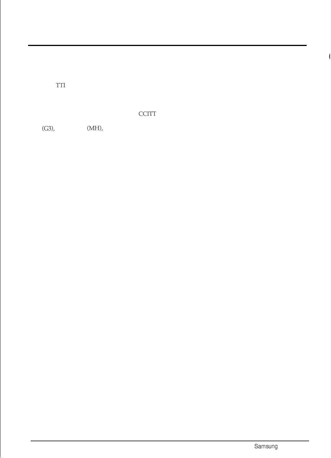
4-1 Handset
l Disconnect the handset cord modular plug from
the machine.
l Remove the two rubber dummies from the
holes and loosen the two screws.
l Push the upper cover in the direction of arrow
to remove.
Figure 4-l
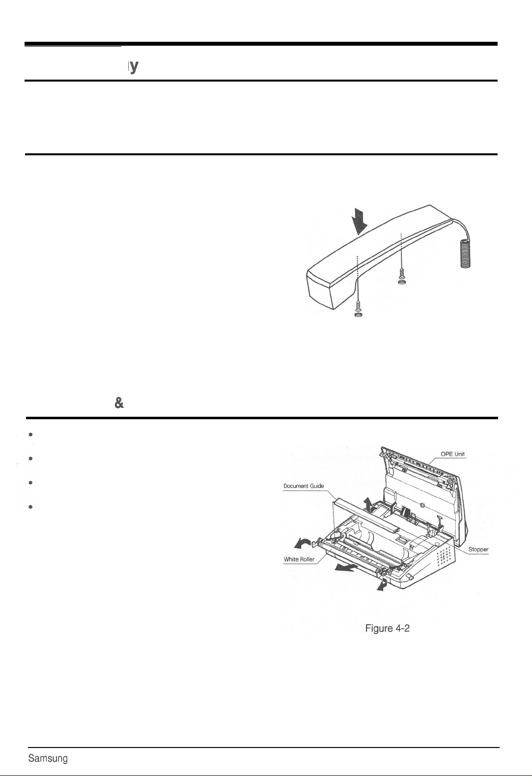
4-2 TX Guide & White Roller
Open the operation unit assembly.
Disengage the stopper.
Remove TX guide.
Remove white roller.
Samsung
Electronics
4-l
Page 10
Disassembly Instruction
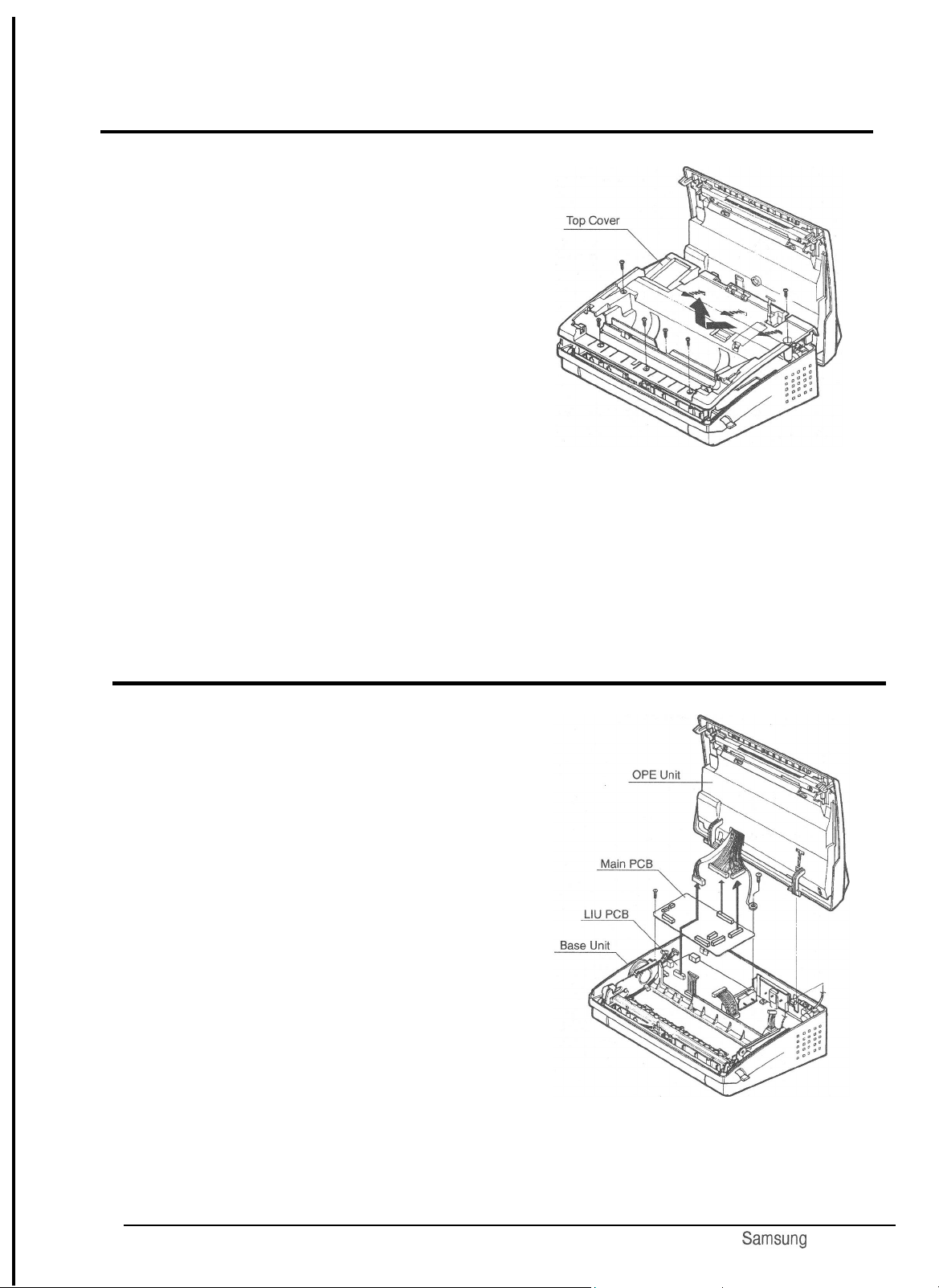
4-3. Top Cover
l Loosen the six screws fastening the top cover.
l Carefully lift the top cover as shown in the
direction of the arrow.
Figure 4-3
4-4. QPE Unit
l Disconnect the harnesses from the Main PBA.
l Loosen the two screws fastening the Main PBA.
l Disconnect the harnesses from the LIU PBA.
l
Remove the OPE unit from the base unit.
Figure 4-4
4-2
Samsung
Electronics
Page 11
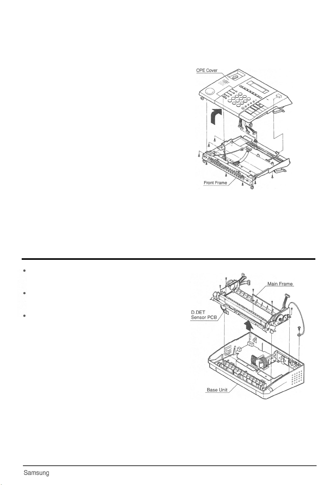
4-4-l. OPE Cover
l Loosen the seven screws fastening the OPE
unit.
l Carefully lift the OPE cover in the direction of
the arrow as shown.
Disassembly Instruction
4-5. Main Frame
Loosen the screw fastening the power supply
and earth harness.
Loosen the five screws fastening the main frame
assembly.
Lift the main frame assembly and D.DET sensor
PBA.
Figure 4-5
Samsung
Electronics
Figure 4-6
4-3
Page 12
Disassembly Instruction
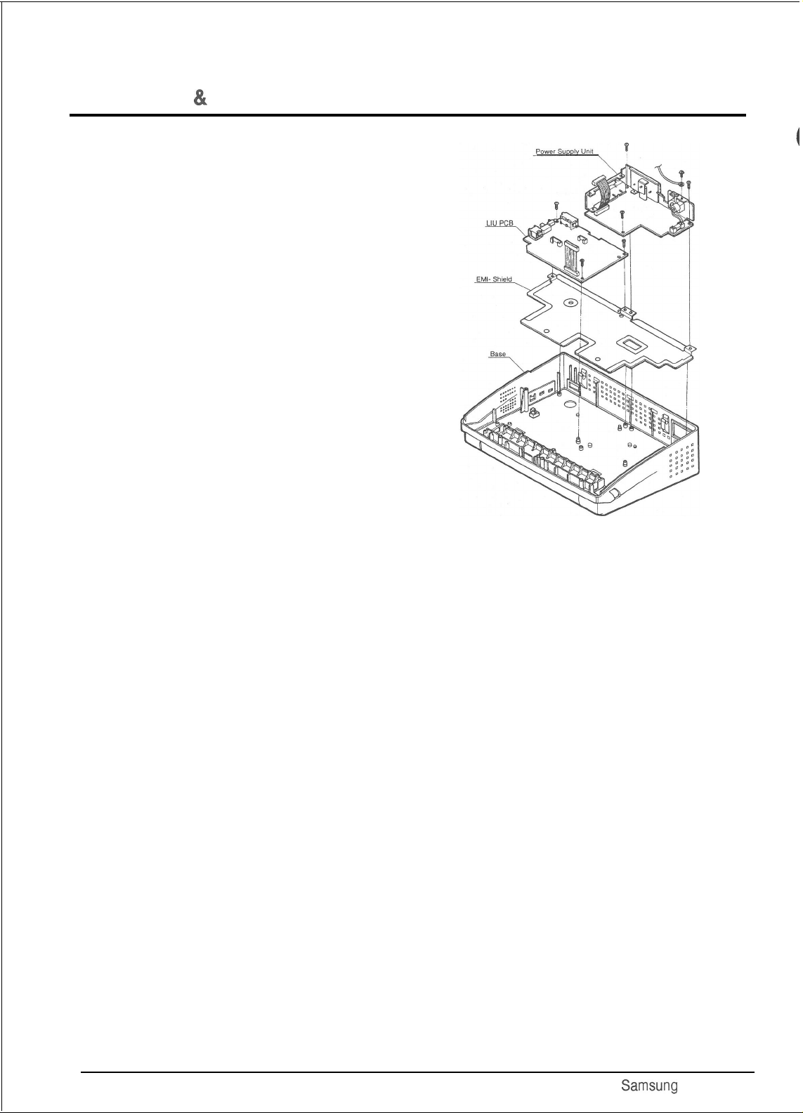
4-6. LIU PBA & POWER SUPPLY
l Loosen the six screws fastening the LIU PBA
and Power Supply unit.
l Lift the LIU PBA and Power Supply unit.
Figure 4-7
4-4
Samsung
Electronics
Page 13
5.
Circui
5-I
General
The main circuit board consists of memory, MODEM, TX- and RX-related circuitry, TAD, and the Integrated
Facsimile Controller (IFC), which includes the CPU and I/O device drivers and controls the system.
5-2 IFC
This circuit consists of the data and address bus, real time clock (RTC), image sensor, motor driver
controller, Thermal Print head controller, IFC including I/O port, and system reset circuit.
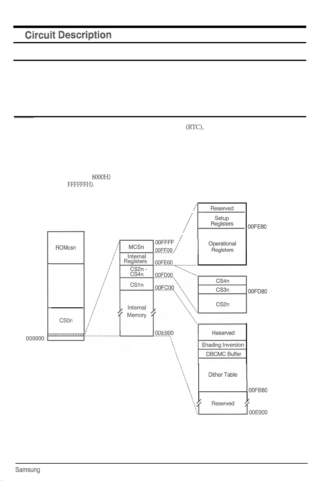
5-2-l Memory Map
The external memory of the CPU is divided into
32kB RAM (OOOOH through
(FFOOOOH through FFFFFFH).
FFFFFF
SOOOH)
and 64kB ROM
1
,,*’
,,**
.*’
,*’
se’
,*’
OOFEFF
OOFEEO
OOFE80
FOOOOO
OFFFFF
ROMcsn
Not
Available
CSOn
OOFEOO
OOFDFF
OOFDCO
OOFD80
OOFDOO
OOFBFF
OOFBEO
OOFBDO
OOFBCO
DitherTable
:
:
:
I
OOFB80
Samsung
Electronics
Figure 5-1: XFC Memory Map
5-1
Page 14
Circuit Description
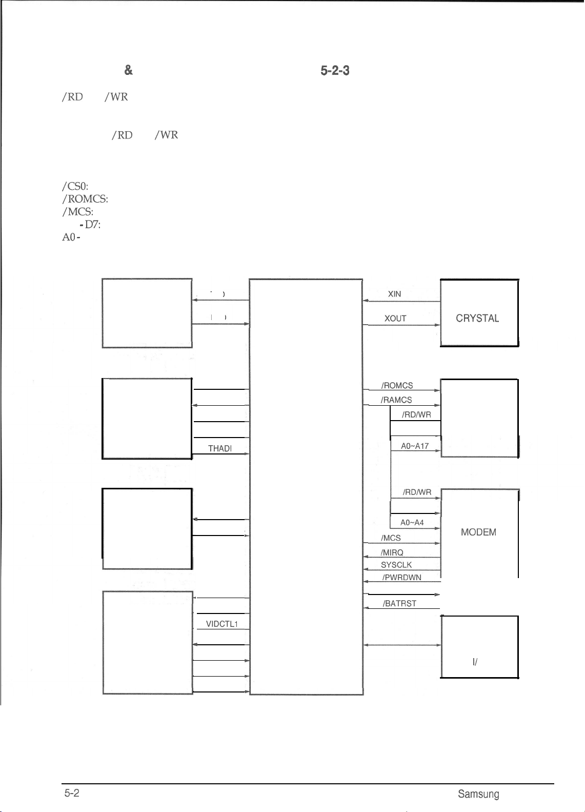
5-2-2 Data & Address Bus Control
/RD
and
/WR
signals are active in the low state,
with TSTCLK high, and an internal wait state
occurs in the TSTCLK (6 MHz). These signals are
sent to the
and the MODEM in order to read or write data
when a chip select line is active.
/CSO:
/ROMCS:
/MCS:
DO -
A0 -
A19: address bus
/RD
and
/WR
ports of RAM, ROM,
RAM chip select active (low)
ROM chip select active (low)
MODEM chip select active (low)
D7:
8 bit data bus
OPERATOR
PANEL
SERIAL
COMMUNICATION
TXD
RXD
5-2-3
System Clock
The 6 MHz internal clock frequency is generated
by dividing the 12 MHz system clock from
MODEM by two inside the MODEM.
Li
Y
RTC
CRYSTAL
PRINTER
DATA
CONTROL
AND
SENSORS
MOTOR
DRIVER
(MOTOR)
SCANNER
CONTROL
AND
PROCESSING
STB O-3
PDAT
I
PCLK
PLAT
THADI
SM o-3
I
MOTOR POS
START
SCLK
VIDCTLl
H/B
1
Vin
+Vref
-Vref
IFC(XFC-B)
IROMCS
IRAMCS
lRD/WR
DO-D7
1
DO-D7
ZkFJ
REST0
/BATRST
J
*
EXTERNAL
BUS
4
MoDEM
*
GENERAL
PURPOSE
I/
0
Figure 5-2: XFC Hardware Interface Signals
Samsung
Electronics
Page 15
Circuit Description
5-2-4 Real Time Clock (RTC)
This circuit receives clock pulses from an external
32.768
kHz
crystal, which it divides into hours,
32768 KHz
-
BUSY FLAG CLEAR
15 BIT
PRESCALER
)
-
DAYS
b
1Hz
BUSY
DETECT
CO=28,29,
30,0r 31
MONTH
DECODER
SECONDS
6 BIT
I
BUSY FLAG
b
MONTHS
d
minutes, seconds, year, month, and day.
A battery maintains operation when power is off.
XFC-B can up-track 32 years, beginning with 1992.
CO=6!J m[
I
CO=“I,“,aI
CO=24,
I
-
4 BIT
co=12
5 BIT
*
YEARS
I I
I
3 STATE
DRIVER
1
Figure 5-3: RTC Block Diagram
5-2-5 Print Control
The PCLK and PDAT signals synchronise serial
print data to the TPH. PLAT latches TPH serial
print data to the TPH from a shift register through
PDAT. STBl - STB4 enable TPH printing in four
sequential intervals.
Print
Cmd
h
PrintLine
(MSINT Caty-out)
Shift Data
Shift Clk
n
Sh D Sh C
This
system has a lOms/Line printing format and
determines
SIB
High/Low enable status
according to the STBPOL signal.
Print
Cmd
A
l-l
I
I
Sh D
Sh C
Samsung
STBl
STB2
Electronics
Figure 5-4: Printer Timing
5-3
Page 16
Circuit Description
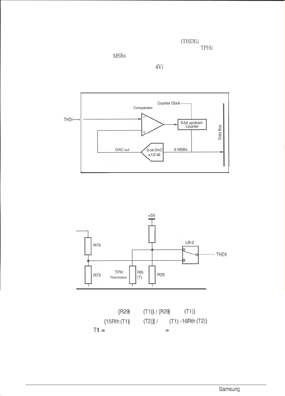
5-2-6 TPH A/D Converter
The ADC is composed of a 6 bit DAC, comparator,
filter, and 9 bit up/down counter. The 6 MSBs of
the 9 bit counter generate a reference signal to the
comparator. TPH temperature or DTAD back-up
voltage is sensed by comparing DAC output
THDI-
voltage to the comparator with the thermistor
input voltage (THDI), which originates as an
output signal from the TPH. It then supplies the
proper strobe pulse to the TPH. The thermistor
input voltage (THDI) operates within a range of 1
to 4v.
Figure 5-5: ADC Block Diagram
Battery
THDl
I I I
GND5
Approximate values (TPH Temperature) of R28 and R29 can be calculated
from the following formulas:
R28 = 0.25 x (R29 x Rth
R29 = (15Rth
(Tl)
(Tl)} /
(R29 + Rth
x Rth (T2)) / {Rth
(Tl)}
(Tl)
-16Rth (T2))
Where Tl = minimum temperature, T2 = maximum temperature.
5-4
Figure 5-6: THD Connection Circuit
Samsung Electronics
Page 17
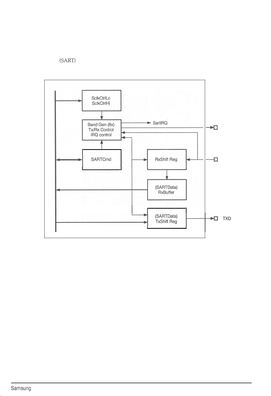
5-2-7 Operation Panel Control
Communication
A Synchronous/Asynchronous
Receiver/Transmitter
transmission between the main circuit board and
the operator panel.
(SART)
CPU Bus
0
controls serial data
b
SARTCmd
-I
Circuit Description
4
SCLK
4
RXD
0 Internal Register
Figure 5-7: SART Block Diagram
I
I
1
Samsung
Electronics
5-5
Page 18

Circuit Description
5-2-8 Image Sensor
The shading wave is formed by scanning the white
roller prior to a document. The slice level is
determined by the shading wave, and
Shading Correction
Shade
RAM= y
FADC 6;
0
.__
I
4
____________________~_______________________________________O
compensates for shading distortion according to
the CIS characteristics. The wave format from the
CIS is converted into a 6 bit digital value in the IFC
image processor, and then processed in B/W or
intermediate mode.
1
:
!
External
Dithering
or
i3Anl
Thresholding
1,
I
@
Inversion Table
@
Shading Enabled
@
Edge Enhancement Enabled
@
Dynamic Background and Contrast Control
/
Enabled
EnaMed (ShTblEnb)
WCC4
(ShadeEnb)
(EdgeEnhEnb)
Figure 5-8: Scanner image Processing Block Diagram
-primaR
- - - - -
Secondary (optional) Paths
Paths
External
Video
Processing
Data input
5-6
Samsung
Electronics
Page 19

Circuit Description
5-2-9 CIS Input
To process the B/W
(+VREF)
and minimum (input signal are controlled by calibrating MUXA
and MUXB in the high state for the maximum
level, and setting them to earth for the minimum
level.
Processor
input signal, maximum
VRE~)
values of the CIS
1
Dither & Shading
1
I
Scanner Image
Processing
I
A.
I
I I ’
I
CPUCLK
c
Scanner
Timing & Control
I
Processing to compensate for CIS shading
distortion is controlled with MUXA ‘low’ and
MUXB high’. For B/W mode, MUXA should be
‘high, and MUXB ‘low’. For half-tone, MUXA is
‘low’, and MUXB is ‘high.
XFC-B ;External Circuits
i................;
i External
;
RAM
:
. . . . . . . . . . . . . . .
Line Buffer
4
:
: . . . . . RAM . . . . .
+
VIOCTL(l:O)
i
:
..f
i
i
Scanner
_$
&I
C;Kl.
: CLKlh, CLKZ
Figure 5-9: Scanner Interface Block Diagram
5-2-10
The CIS driver clock frequency is 250
duty cycle is used to lengthen the charging time. A
CIS Driver
CLOCK
SI
SIG
kHz.
A 75%
250 KHZ (L:DUTY 75%)
-
~________________________________________________~
1
LINE
start signal is provided every 10 ms to match the
line scanning time. Actual image signal is
provided in less than 6.8 ms, using the 250
clock and taking A4 paper size into consideration.
kHz
r-l
Samsung
Electronics
5-7
Page 20

Circuit Description
5-2-11
IN NO 1 PIN NAME 1 CIRCUIT NAME ( I/O
-it-k%-
79 1
I/O
94
93
I
90 1
89
87
86 )
85
84
83
80
GPIO
I
78 1
GPIO
I
76
1
75
118
Port Table
GPIO
0
GPIO
1
RING-DETECT I
I
GPIO
4 1
GPIO
5
GPIO
6
GPIO
7 1
GPIO
8
GPIO
9
GPIO IO
GPIO
12
13
1
I I
14
1
I
GPIO161
GPIO
17
GPO 0
SPK_CTL
CMLl_CTL
DSP_HL
DSP_ACK
TX_CTRL
MODE_DET
ADIN_CTRL
MlC_ON
REC_CTRL
SIO CLK
TXD
RXD
DSP_RST
DSP_FLAG
+24V
0
0
I
DOC_DET 1
0
0
I SlO I
/ SIO /
I I /
1
I
I
ON “; 0 TPH POWER
1
0
0
I
MODE DETECT SENSOR OPEN MODE DETECT SENSOR CLOSE
I
1
0
SIO
I
0
1
ACTIVE STATE (H)
SPEAKER DISABLE
CML RELAY ON (FAX)
DSP HIGH BYTE SELECT
MODEM TX PATH DSP OGM TX PATH
TPH TEMPARATURE CHECK
MIC. OFF
ICM RECORD PATH ICM RECORD PATH
OPE MICOM TX
/
DTAD BACK-UP BATTERY CHECK
I
I
DSP RESET
DSP DATA PUMP DISABLE DSP DATA PUMP ENABLE
(+24
V) ON TPH POWER
ACTIVE STATE (L)
SPEAKERENABLE
CML RELAY OFF (TEL)
DSP LOW BYTE SELECT
RING DETECT
DSP ACKNOWLEDGE
MIC. OFF
OPE MICOM TX
(+24
V) OFF
116
115
106 1 GPO4
GPO2
GPO 3
I
105 1 GPO5
104
103
GPO
GPO
6
7
VOL_A
VOL_B
VOL_C
I
1
MPA
1
MPB
IMPA 0
/MPB
I I
/
0
I 0 I
0
VOLC 1 VOLB 1 VOLA
I L I L
L
I
MOTOR PHASE A
1
MC14051 OUTPUT
KEYCLICK
ON
MOTOR PHASE B
MOTOR
MOTOR
PHASE
-A
PHASE- B
5-8
Samsung
Electronics
Page 21

Circuit Description
5-2-l 2 Motor Controller
The SFllOT performs sending, receiving, and
printing functions utilising a single 24 volt motor.
This motor has a 150 ohm winding resistance.
Three drive strobe pulses operate the motor.
Table
5-11:
Motor Functions
Motor Function Drive Strobe Pulse
Swing Gear Control
Document Out
Super Fine Mode
Other
’
100
pps
1oopps
1oopps
1oopps
icik fTSTCLKl
Watchdog Reset
Phase
2 phase
2 phase
1-2 phase
2 phase
5-2-l 3 Miscellaneous Signals
The key click consists of an 800 Hz tone of 20 ms
duration.
/REST0
drives MODEM (/PORI), UART
(/POR)
and serves to reset the MODEM, UART.
/MIRQ
is the MODEM interrupt signal.
5-2-l 4 Reset
Two power resets and a watchdog timer in the IFC
comprise the elements of this circuit. Battery
power reset
battery-powered logic, and primary power reset
(/PWRDWN)
logic when system power is supplied.
(/BATRST)
is used to initialise the
initialises non-battery-powered
IPWRDWN
BATRSTn
POW.3
DOWFl
NMI
Power up Delay 1
(l-2
Reset clocks)
reset
AA
7!ikgj=
‘_ .
Figure
POWER MONITOR
If 5V power to
and
4.35V
indicated and the output of
(GND). This causes the IFC to become active
(‘low’=reset).
IFC/RESET terminal to be reset. The output
terminal of
configuration, and is connected to PFC through a
10k
pull-up resistor.
KIA7045P
(typically
drops to between 4.65
4.5V),
power failure will be
KIA7045P
The IFC reset causes the MODEM
KIA7045P
is an open-drain
512:
Power Reset Block Diagram
will go ‘low’
ESETn
R?S”
t
-
cson
--c
Power*up
Delay 2
To
Internal logic -
Clock enable
to battery (BackupConlig) register reset
WATCH DOG TIMER
This programmable counter in the IFC is reset
every 2 ms. If not reset after 250 ms, the system is
automatically reset and switches to initialise mode.
BATTERY POWER RESET
When battery power (VB) is applied to IFC the first
time,
causing a reset to occur.
VB CUrrent reSU&S in /BATRST
going ‘low’,
Samsung
Electronics
5-9
Page 22

Circuit Description
5-3 Memorv
System memory consists of 64kB ROM and 32kB RAM. All of RAM is backed up. ROM and RAM are
selected by chip select lines, and data is accessed by the units position of the byte.
+5V
power is applied to RAM through VB. The SFllOT model facsimile machine uses a
lk
resistor in series with the positive battery terminal is for battery protection.
Li(thium)
battery. A
5-4 Modem and TX- and RX- Related Circuits
These circuits control signal transmission between the internal MODEM and the LIU or a remote MODEM.
The R96DFXL MODEM is a single-chip fax-MODEM having features to detect and generate DTMF tones.
TX OUT is the MODEM output port, and RX IN is the input port.
MODEM initialisation at system power on. DO - D7 are data buses. RSO- RS4 are internal register select
signals which determine the mode.
/MCS
is the chip select signal,
control signals. RLSD is used for v.24 interface-related signals and
Refer to Figure 5-14 for available R96DFXL I/O ports.
/PORI
is the IFC signal which enables
/RD
and /WR are the read and write
/MIRQ
is the MODEM interrupt.
PIN NO PIN NAME CIRCUIT NAME
100
1
2 / GP 04 1
3 1 GP 05
4 I GPO6
5
63
61
75
76
94
93 1 GP 20
91
I
GP 02
GP 03
GP
07
GP
11
GP 13
GP 16
GP 17
GP 19
GP 21
HT_BI
HOOKDET2 I
OFF_RST 1
1
I
I
RX_CTRL
_GLED
1
-
I/O ACTIVE STATE (H)
0
0
I
1
, ,
I
I
0
0
I
I
I
I
I
I
1
I
/
I I
HALFTONE MODE
OPE RESET
RX PATH REMOTE PATH
CIS LED ON CIS LED OFF
DESCRIPTION
BINARY MODE
EXTERNAL TEL. IN USE
I
5-10
Samsung
Electronics
Page 23

5-4-l Transmit Circuit
5-4-2
Receive Circuit
Circuit Description
This circuitry controls transmission of analog
signals from the MODEM. Output voltage from
the MODEM is buffered through the LIU board
and OP amp after signal smoothing and filtering,
and finally output to the line.
5-5
TAD
TAD circuit consists of a voice coprocessor to record and play voice messages in voice memory.
5-5-l Recording Path
R55 provides power to the condenser microphone.
Voice signal from the microphone is passed
through active filter U15, R117 and C96, R82, C58
to clear aliasing noise occuring while sampling
and amplifying the signal. Q5 and Q2 compose
ALC (Automatic Level Control) circuit. CODEC
(U22)
converts the voice signal to digital and
converts the digital signal from voice coprocessor
into analog for line output.
In receive mode, analog signals from the LIU
board are transferred to RX IN through the BPF
and smoothing filter.
5-5-3 Line Input and Play Path
Incoming signals from line are stored in the voice
memory (4 M DRAM) through CODEC and DSPG
DRAM controller. When played, DSPG processes
the data stored in voice memory and sends it out
to LIU through CODEC and
through the speaker, DSPG sends the signal to
speaker through
amp.
R108,
MUX
R108.
To playback
(U12, U14),
and op
5-5-2 Mic Input Path
Transmit path functions as MIC input path.
Outgoing messages and memo messages from
CODEC are stored in the voice memory (4 M
DRAM) through the DSPG DRAM controller.
5-5-4 DSPG
This circuit consists of Host Interface, Memory
Interface, CODEC Interface, and DSP core. Host
Interface sends and receives data to and from IFC.
Memory Interface sends and receives the
compressed voice data to and from DRAM to play
back and record voice data. DSP core
communicates with host IFC through Host
Interface.
5-5-5 Voice Backup
+5V
is supplied for voice memory through VBT
when power is on. When power is off,
supplied from the 9V backup battery.
+5V
is
Samsung
Electronics
5-11
Page 24

Circuit Description
5-6 LIU PBA
The LIU (Line Interface Unit) interfaces the MODEM and telephone to the telephone line. The FAX and
telephone portions of the LIU are active with machine power on. When machine power is off, only the
telephone circuitry operates, powered by telephone line voltage. The FAX portion of LIU consists of the
interface between MODEM and telephone line, and the circuits for DC loop feeding, DP signal, loop current,
and ring detect. The telephone portion is divided into ringer, dialling, and speech circuits. Refer to the
Schemetic and Wiring Diagram sections of this manual. Refer to LIU circuit and Block Diagrams.
5-6-l FAX section
MODEM/ LINE INTERFACE
This is the path for data and remote control
signals.
l CML201 relay: switches telephone line between
FAX and telephone circuits.
l
U201
pin 3 TIT (Telephone Input Transformer):
Single ended input from transformer (T202).
l
U201
pin 3 ROT (Receive Output Transformer):
Output for driving transformer
AC impedance larger than 10 kohm.
l
C202:
DTMF and CNG detect path to
kohm winding under idle conditions and DC
blocking for 20 kohm winding.
l AC impedance: The AC impedance of
LIU) is set to 1000 ohm by external capacitor
(C215) at
U201
pin 8 CI (Complex Impedance
input) port. With external resistor (R249) at
pin 34
AC1
port it can be programmed to 600
ohm.
U201
pin 35 CS (Current Shunt control
output) port is an N-channel open-drain output
to control the external high power shunt
transistor for synthesizing AC and DC
impedances.
l DC conditions: Normal operating mode is from
15 mA to 100
mA.
An operating mode with
reduced performance is 5 mA to 15
line hold range from 0 mA to 5
in a power down mode and the voltage at
pin 37 LI (Line Input) port is reduced to a
maximum of 3.5 V. The DC characteristic is
determinedby the voltage at
and a R215 resistor between
Pin 39 LS port. It can be calculated by the
equation:
VLs
=
VLI
+
ILINE
x
I3215
(T203)
mA.
mA,
the device is
U201
pin 37 LI port
U201
pin 37 LI and
with an
T20120
U201 (I-
In the
U201
U201
RING DETECT
U201
pin 28 (MO) is the ring tone output port and
drives Q207, which drives FET202 and the piezo
buzzer. The driving signal of the piezo buzzer is
applied to photo coupler
LLC (Line Loss
Compensation)/LOOP
U204.
CURRENT DETECT
l The LLC is a pin option. When activated, the
transmit and receive gains for input and output
are decreased by 6
when
U201
pin 31 LLC is connected to AGND
dB.
Line current is 20 mA
and 75 mA when this pin is connected to Vcc.
The LLC is deactivated when LLC pin is
connected to Vss.
l When the CML201 relay or hook switch
switches to telephone line,
U201
on the LIU
board and U6 on the Main board start
communication.
U201
sends
<Ack>
message
which contains line current information. Using
this line current information, Main CPU can
recognize a parallel phone.
SERIAL INTERFACE
l
U201
pin 11 RXD : Schmitt triger input
(threshold = 2.5 V) to serial interface.
l
U201
pin 29 TXD : Open-drain output from
serial interface.
l The communication is via a standard
Baud Rate 9600
Start Bit 1
Stop Bit 1
Date Bits 8
Parity Bit None
LSB is transferred prior to MSB
UART:
5-12
Samsung
Electronics
Page 25

Circuit Description
5-6-2
Telephone Section
RINGER CIRCUIT
. When a ringing voltage is sensed on the line,
Vcc of
U201
(I-LIU) is charged via an external
path. When operating voltage is reached, the
oscillator starts and
frequency. After a valid ring frequency is
applied to the
Discrimination) port, the ring tone generator of
U201
sends out a 3-tone melody via
MO (Ring Melody Output) port.
l
U201:
I-LIU and associated components.
0
Ring frequency passes through DC blocking
capacitor
C201
Austria) and zener diode
Switzerland or Austria) to
port.
.
Line ring AC voltage passes through DC
blocking capacitor
R203,
diode bridge BD201, CML relay and hook
switch to FET202
R226.
l The ring frequency discriminator of
assures that only signals with a frequency
between 13 Hz and 70 Hz are regarded as valid
ring signals.
l When a valid ring signal is present for 73 ms
continuously, the ring melody generator (pin 28,
MO) is activated and remains active as long as a
valid ring signal is present.
l
U201
filters the ring signal and applies it to
output pin 28 (MO). This is the piezo buzzer
drive signal.
l The 3 basic melody frequencies are:
F2 = 1067 Hz and F3 = 1333Hz. The repetition
rate is set to 4 which means that the sequence of
Fl,
F2, F3,
Fl,
second.
U201
detects the ring
U201
pin 25 RFD (Ring Frequency
U201
pin 28
or C234 (for Switzerland or
ZD205
or ZD209 (for
U201
pin 25 RFD
C201,
current limit resistor
(BS170)
pin3, C217,ZD207 and
U201
Fl
= 880 Hz,
F2, F3 is repeated 4 times per
Current Sense Input).
DP DIAL
-
U201
pin 2
(DMS)
is set to Vcc
(40/60)
l Dial pulses originate at
by R227 or R228.
U201
(33/67)
pin 27
or Vss
(DPn),
which toggles Q205, driving Q201. The resulting
intermittent voltage interrupts the telephone
line.
l Pulse MB ratio is set by
Vcc = 33:67, and Vss =
l
U201
pin 35 CS port: Modulation and shorting
U201
40:60.
pin 2 MDS port.
the line during make period of pulse dialling.
SPEECH CIRCUIT
l
U201
(STI9510) and associated components.
l Handset transmitter circuit
Transmit (condenser mic.) of handset is filtered
by R213, R242,
C225, C231, C232 and C246, and then amplified
by
U201
pins 32 and 33 (Ml,
0
Handset receiver circuit
Dynamic recever of handset is filtered by R245,
C226, C227, C228 and C248, and then applied to
U201
pin 1
0 U201
pin 39
line.
SIDETONE
l Sidetone audio characteristics are controlled by
R217, R218, C212, and C214, connected to
pin 7 STB.
R243,
R244, C221, C223, C224,
M2).
(ROH).
(LS)
is audio output to telephone
CIRCUIT
U201
MF DIAL
l
U201
pin 2 DMS (Dial Mode Selection) port is
set by T/P switch
l MF signal appears (tone level of low group:
typical -14
dBm)
Generator Output). This signal is
R248,
R250
and C235, then to Amplifier
pin 9
MFI
(DTMF Amplifier Input).
l Line dial signals appear at
Samsung
Electronics
(SW202).
at
U201
pin 4 MFO (DTMF
levelled
U201
pin 39 LS (Line
by
U201
5-13
Page 26

Circuit Description
5-7 OPE PBA
OPE PBA consists of
Refer to OPE Circuit and Block Diagrams.
0
Signals from the key matrix are delivered to
l Connector I’4 is NPO (No Power Operation) key matrix output.
l
U300
pin 4 (RX DATA) is UART data to MAIN PBA.
l Display from controller is received at
. LCD drive signals are
l Machine status LED drive signals are
l Paper empty sensor staturs delivers to
Paper
Empty
Sensor
I
U300
t-----+
I
(MICOM
U300 P2-X
Z8601),
pin group, connector pin
LCD, key matrix, LED indicators, and the paper empty sensor.
U300
X/Y input pin group
U300
pin 5 (TX DATA).
U300
PO-X pin group.
U300
pin 39. (High: paper empty, Low: paper exists).
P2-1 - P2-3.
i
#‘l-X).
Connector
MICOM
Z-8601
Reset
~
I
3
-+---+I
LEDs
Figure 5-13 OPE Block Diagram
5-14 Samsung
Electronics
Page 27

7 Electrical Parts List
7-1 MAIN PBA
Capacitor / Resistor tolerance:
D:
0.5%,F:1%, G: 2 %,J:5 %,K:10 %, M:20%, Z:
+80%,-20 %
I
I I
I
I
I 1
1 1
L
I I
C25
Ref. No.
I
1
Cl
c2.
c3
c4
c5
C6
c7
C8
c9
Cl0
Cl1
Cl2
Cl3
Cl4
Cl5
Cl6
Cl7
Cl8
Cl9
c20
c21
c22
C23
1
C24
C26
C27
C28
C29
c30
c31
C32
c33
1
PBA, PCB Assembly, MAIN
-
Capacitors
1
Ceramic, Chip, 680
Ceramic, Chip,
Ceramic, Chip,
Ceramic, Chip,
Ceramic, Chip,
Ceramic, Chip,
Ceramic, Chip,
Ceramic, Chip,
Ceramic, Chip,
Ceramic,
1
Ceramic,
I Ceramic, Chip, 100
Ceramic, Chip,
Ceramic, Chip,
Ceramic, Chip,
Ceramic, Chip,
Ceramic, Chip,
I
Ceramic, Chip, 100
Ceramic, Chip,
Ceramic, Chip,
Ceramic, Chip,
Ceramic, Chip,
1
Ceramic, Chip, 100
Ceramic, Chip, 100
I
Ceramic,
Ceramic, Chip,
Ceramic, Chip,
Ceramic, Chip,
Ceramic, Chip,
Ceramic, Chip,
Ceramic, Chip,
Ceramic, Chip,
Ceramic, Chip,
Chip,
Chip,
Chin,
Description
pF,
680
pF,J,50
680
pF,J,50
680
pF,J,50
680
pF,J,50
100
pF,J,50
100
pF,J,50
680
pF,
680
pF,
100 nF,
100
nF,
nF,
100 nF,Z,50
100 nF,Z,50
100 nF,Z,50
100 nF,Z,50
100 nF,Z,50
nF,
100 nF,Z,50
100 nF,Z,50
100 nF,Z,50
100 nF,Z,50
nF,
nF,
100
nF,
100 nF,Z,50
100 nF,Z,50
100 nF,Z,50
100 nF,Z,50
100 nF,Z,50
100 nF,Z,50
100 nF,Z,50
100 nF,Z,50
J, 50 V
J, 50 V
J, 50 V
Z, 50 V
Z, 50 V
Z, 50 V
Z, 50 V
Z, 50 V
Z, 50 V
Z, 50 V
SEC Code Remark
I2203-001132
V
V 2203-001132
V
V 2203-001132
V 2203-000239
V 2203-000239
V
V
V
V
V 2203-000192
V 2203-000192
V 2203-000192
V
V
V
V
V 2203-000192
V
V
V 2203-000192
V 2203-000192
V
2203-001132
2203-001132
2203-001132
2203-001132
2203-000192
1
2203-000192
1
2203-000192
2203-000192
2203-000192
2203-000192
2203-000192
1
2203-000192
2203-000192
2203-000192
I2203-000192
I2203-000192
I
2203-000192
2203-000192
2203-000192
2203-000192
2203-000192
2203-000192
I
1
1
1
1
l
I
I
Samsung
Electronics
7-l
Page 28

Electrical Parts List
)
Ref. No.
I
c34
c35
1 1
C36
I I C37
C38
c39
c40
c41
C42
I I C43
I
ICJJ
c45
C46
c47
C48
I I C49
I I
C50
c51
C52
c53
c54
1
c55
I I
C56
I I C57
C58
c59
C60 Electrolytic,10pF,M,25V,GP
C61
C62 Electrolytic,10@,
I I
C63
C64
1
C65 Electrolytic, 2.2
C66
1
C67
I
IO3
C69
c70
c71
C72
c73
c74
c75
1
Ceramic, Chip,
Ceramic, Chip,
)
Ceramic,
1
Ceramic, Chip, 100
Chip,
Ceramic, Chip,
Ceramic,
Chip,
Ceramic, Chip,
Ceramic, Chip,
Ceramic, Chip,
I
Ceramic,
)
Ceramic,
Chip,
Chip,
Ceramic, Chip,
Ceramic, Chip,
Ceramic, Chip,
Ceramic, Chip,
I
Ceramic,
I
Ceramic,
Chip,
Chip,
Ceramic, Chip,
Ceramic, Chip,
Ceramic, Chip,
Ceramic, Chip,
1
Ceramic, Chip, 100
1
Ceramic,
)
Ceramic,
Chip,
Chip,
Ceramic, Chip,
Electrolytic,
Description
100
100 nF,Z,50
100
A
100 nF,Z,50
100 nF,Z,50
100 nF,Z,50
100 nF,Z,50
100 nF,Z,50
100
100
100 nF,Z,50
100 nF,Z,50
A
100 nF,Z,50
100 nF,Z,50
100
100
100 nF,Z,50
100 nF,Z,50
100
100
22
pF,
22
pF,
470
10
LIF,
M, 25 V, GP
nF,Z,50
nF,
nF,
nF,
nF,
nF,
nF,
nF,
pF,
pF,
pF,
Electrolytic,10+IF,M,25
M,25V, GP
I
Electrolytic, 10
1
Electrolytic,10pF,M,25
Ceramic, Chip,
1
Ceramic, Chip, 100
I
Electrolytic, 100
Electrolytic, 100
Electrolytic, 33
Ceramic, Chip, 1
Ceramic, Chip,
Ceramic, Chip,
Ceramic, Chip, 100
Electrolytic, 1
vF,
M, 25 V, GP
pF,
M, 16 V, GP
22
pF,
pF,
~.IF,
M, 16 V, GP
pF,
M, 16 V, GP
+IF,
M, 35 V, GP
nF,
100 nF,Z,50
100 nF,Z,50
A
pF,
pF,
M, 50 V, GP
Z, 50 V
Z, 50 V
Z, 50 V
Z, 50 V
Z, 50 V
Z, 50 V
Z, 50 V
J, 50 V
J, 50 V
J, 50 V
J, 50 V
J,50V
V, GP
V, GP
J, 50 V
J, 50 V
K, 50 V
J, 50 V
SEC Code
V
V
V
V
V
V
V
V
V
V
V
V
V
2203-000192
2203-000192
1
2203-000192
)
2203-000192
2203-000192
2203-000192
2203-000192
2203-000192
2203-000192
)
2203-000192
1
2203-000192
2203-000192
2203-000192
2203-000192
2203-000192
1
2203-000192
(
2203-000192
2203-000192
2203-000192
/
/
1
/
/
I
Remark
2203-000192
2203-000239
)
2203-000239
1
2203-000634
1
2203-000634
1
)
2203-000953
2401-000448
2401-000448
2401-000448
2401-000448
1
2401-000448
I
1
2401-000448
I
I
2401-000629
2203-000634
1
2203-000239
I
2401-000042
I
2401-000042
2401-001185
2203-000444
V
V
2203-000192
2203-000192
2203-000239
2401-000597
7-2
Samsung
Electronics
Page 29

Electrical Parts List
1
Ref. No.
C76
c77
I
I C78
c79
C80
1
1~331
C82
C83
C84
C85
C86
C87 Ceramic, Chip, 270
C88
C89 Ceramic, Chip, 18
I I
C90
1
c91
C92
c93
c94
c95
1
C96
I I C97
I I
C98
I
c99
Cl00
Cl01
1
Cl02
I I
Cl03
Cl04
Cl05
Cl06
Cl07
Cl08
1
Ceramic, Chip,
Ceramic, Chip,
1
Ceramic, Chip, 100
Ceramic, Chip,
Ceramic, Chip,
1
Ceramic, Chip, 1
Ceramic, Chip, 1
Ceramic, Chip, 47
Electrolytic, 1
Electrolytic, 1
Electrolytic, 1
Ceramic, Chip, 39
I
Ceramic,
1
Ceramic, Chip, 10
Ceramic, Chip,
Ceramic, Chip,
Electrolytic, 22
Ceramic, Chip,
1
Ceramic, Chip, 47
I
Ceramic,
1
Ceramic, Chip, 1
1
Ceramic, Chip, 1
Ceramic, Chip,
Ceramic, Chip,
1
Ceramic, Chip, 1
1
Ceramic, Chip, 1
Ceramic, Chip,
Ceramic, Chip,
Ceramic, Chip,
Ceramic, Chip,
Ceramic,
Chip,
Chip, 100
Chip,
Description
1
nF,
68
nF,
1
nF,K,50
1
nF, K, 50
nF,
nF,
nF,
pF,
M, 50 V, GP
pF,
M, 50 V, GP
pF,
M, 50 V, GP
pF,
pF,
100
pF,
10
120
pF,
M, 25 V, GP
47
IIF,
nF,
nF,
_
10
1
nF,
nF,
nF,
1
nF,
1
nF,
1
nF,
100
1
nF,
K, 50 V
K, 50 V
nF,
Z, 50 V
K, 50 V
K, 50 V
K, 50 V
pF,
J, 50 V
J, 50 V
J, 50 V
nF,
Z, 50 V
0.5
pF,
0.5
pF,
J, 50 V
nF,
K, 50 V
K, 50 V
nF,
Z, 50 V
K, 50 V
K, 50 V
pF,
0.5
K, 50 V
K, 50 V
K, 50 V
K, 50 V
K, 50 V
K, 50 V
pF,
J, 50 V
K, 50 V
V
V
pF
pF
pF
SEC Code
2203-000444
2203-001142
I2203-000192
2203-000444
2203-000444
(
2203-000444
2203-000444
2203-000979
2401-000597
2401-000597
2401-000597
2203-000661
2203-000858
2203-000429
I2203-000192
I2203-001463
2203-001463
2203-000316
2401-000943
2203-000979
1
2203-000979
I2203-000192
/2203-000444
I
I
2203-000444
2203-001463
2203-000444
1
2203-000444
~2203-000444
2203-000444
2203-000444
2203-000444
2203-000239
2203-000444
Remark
1
1
l
l
I
I
l
I
I
I
I
I
Samsung
Electronics
Page 30

Electrical Parts
List
u9 Op
UlO
Ull
u12
u13
u14
MODEM,
Op amp,
Analog Switch,
OP amp,
Analog Switch,
amp,
4558 1201-000189
R96DFXL
4558 1201-000189
MC14053B
4558 1201-000189
MC14053B
1205-000246
1001-000172
1001-000170
Samsung
Electronics
Page 31

Electrical Park List
Ref. No.
u15 OP amp, 4558
U16
u17
U18
u19
u20
u21
1
u22
U23
Rl
R2
R3
R4
R5
R6
R7
R8
R9
RlO
Rll
R12
R13
R14
R15
R16
R17
R18
R19
R20
R21
R22
R23
R24
I
Im5
R26
IR27
R29
R30
R31
1
R32
Description SEC Code
*
Audio amp, MC34119
CMOS Logic,
CMOS Logic,
CMOS Logic,
74HC245
74HC32
74HCOO
DSP, 16 bit, D6305BllAQA
DRAM, 44C1000,lM x 4 bit
1
CODEC,
I
Andlog Switch,
-
Resistors
Chip, 10 kohm, J,
Chip,
Chip,
Chip, 10 kohm, J,
Chip, 100 kohm, J,
Chip, 10 kohm, J,
Chip, 10 kohm, J,
Chip, 10 kohm, J,
Chip, 10 kohm, J,
Chip, 10 kohm, J,
Chip, 10 kohm, J,
Chip, 1 kohm, J,
Chip,
Chip, 20 ohm, J,
Chip,
Chip, 10 kohm, J,
Chip, 10 kohm, J,
Chip, 10 kohm, J,
Chip, 10 kohm, J,
Chip, 10
Chip, 47 kohm, J,
Chip, 15 kohm, J,
Chip, 10 kohm, J,
Chip,
1
Chip, 10 kohm, J,
I
1
Chip, 10 kohm, J,
1
Chip, 10 kohm, J,
(
Chip,
Chip, 46.4 kohm, F,
Chip, 220 ohm, J,
Chip, 220 ohm, J,
1
Chip, 220 ohm, J,
TP3054J
TC4S66FT
-
10 kohm, J,
10 kohm, J,
10
kohm,
J, 1
10 kohm, J,
kohm, J,
82 kohm, J,
20 kohm, J,
l/10
W
l/10
W
l/10
W
l/10
W
l/10
W
l/10
W
l/10
W
l/10
W
l/10
W
l/10
W
l/10
W
l/10
W
/lO
W
l/4
W
l/10
W
l/10
W
l/10
W
l/10
W
l/10
W
l/10
W 2007-000300
l/10
W
l/10
W
l/10
W
l/10
W
l/10
W
l/10
W
l/10
W
l/10
W
l/10
l/10
W
l/10
W
l/10
W
W
1201-000189
1205-000105
0801-000696
0801-000411
0801-000792
0904-001068
1105-000133
I
1
1205-000120
I
1001-000133
2007-000300
2007-000300
2007-000300
2007-000300
2007-000282
2007-000300
2007-000300
2007-000300
2007-000300
2007-000300
2007-000300
2007-000468
2007-000300
2007-001289
2007-000300
2007-000300
2007-000300
2007-000300
2007-000300
2007-000941
2007-000409
2007-000300
2007-001208
1
2007-000300
I
2007-000300
2007-000300
I
2007-000546
2007-000917
2007-000572
2007-000572
1
2007-000572
Remark
I
I
1
I
1
Samsung
Electronics
7-5
Page 32

Electrical Parts List
R69
R70
R71
R72
R73
R74
R75
R76
Chip, 39 kohm, J,
Chip, 7.5 kohm, J,
Chip, 6.2 kohm, J,
Chip, 1.2 kohm, J,
Chip, 330 kohm, J,
Chip, 330 kohm, J,
Chip, 220 ohm, J,
Chip, 1 Mohm, J,
l/10
l/10
l/10
l/lOW
l/10
l/10
l/10
l/10
W
W
W
W
W
W
W
2007-000830
2007-001141
2007-001055
2007-000221
2007-000757
2007-000757
2007-000572
2007-000477
7-6 Samsung Electronics
Page 33

Electrical Parts List
Samsung
Electronics
7-7
Page 34

Electrical Parts List
I
Ref. No. Description
R120 Chip, 33 kohm, J,
R121 Chip, 15 kohm, J,
R122 Chip, 220 ohm, J, 1 / 10 W
I I
Ql
Q2
Q3
Q4
Q5
1
PCB
SEC Code
l/10
W 2007-000774
l/10
W 2007-000409
2007-000572
-
Transistors -
Small Signal, KSA1182, PNP
Small Signal, KSC2982, NPN 0501-000342
Small Signal, KSC5019, NPN
Small Signal, KSA1182, PNP
Small Signal, KSA1182, PNP
-
Miscellaneous -
PCB, MAIN, Blank
0501-000279
0501-000385
0501-000279
0501-000279
Remark
I
Samsung Electronics
Page 35

7-2.
QPE PBA
1
Ref. No.1 Description
ASSEMBLY, OPE
-
Capacitors
C302
c303
c304
c305
1 ) C306
I I
c307 1
C308
c309
c310
1
C311
1 )
C312
1 1
D304
D305
D306
D307
1 1
D308
I
LED301I LED, Chip, Green, 60 mW, 2 V
I
LED302I LED, Chip, Red, 60 mW, 2 V
)
LED303I LED, Chip, Red, 60 mW, 2 V
LED304
R301
1 1 R302
R303
R304
R305
R306
1 1 R307
1 1 R308
R309
R310
R311
1 1
R312
1
R313
R314
R315
1 1
R316
Ceramic, Chip,
Ceramic, Chip,
Ceramic, Chip,
Ceramic, Chip, 100
1
Ceramic,
Ceramic, Chip, 100
Ceramic, Chip,
Ceramic, Chip,
Ceramic, Chip,
1
Ceramic, Chip, 22
I
Electrolytic, 10
-
Diodes
I
Switching, MMSD914Tl
Switching,
Switching,
Switching,
I
Switching, MMSD914Tl
LED, Chip, Red, 60 mW,2V
-
Resistors
1
Chip, 22 kohm, J,
I Chip,
Chip, 200 ohm, J,
Chip, 0 ohm, J,
Chip, 22 kohm, J,
Chip, 22 kohm, J,
I
Chip, 22 kohm, J,
1
Chip, 10 kohm, J,
Chip, 22 kohm, J,
Chip, 22 kohm, J,
Chip,
10 kohm, J,
I
Chip,
22 kohm, J,
1
Chip, 200 ohm, J,
Chip, 22 kohm, J,
Chip,
1
Chip,
-
100
47
47
Chip,
100
22
100
22
pF,
-
MMSD914Tl
MMSD914Tl
MMSD914Tl
-
22 kohm, J,
l/8
680 ohm, J,
330 ohm, J,
1
SEC Code
JF92-00779A
pF,
K, 50 V 2203-000228
pF,
J, 50 V 2203-001005
pF,
J, 50 V 2203-001005
nF,
M, 50 V
pF,
K, 50 V
nF,
M, 50 V
pF,
J, 50
V
nF,
M,50V
pF,
J, 50
V
pF,
J, 50 V
M, 25 V, GP
l/8
W
l/8
W
l/8
W
W
l/8
W
l/8
W
l/8
W
l/8
W
l/8
W
l/8
W
l/8
W
l/8
W
l/8
W
l/8
W
l/8
W
l/8
W
2203-001452
1 2?03-000228
1
2203-001452
2203-000636
2203-001452
2203-000636
1
2203-000636
j
2401-000448
1
0401-000116
0401-000116
0401-000116
0401-000116
1
0401-000116
1
0601-000011
1
0601-000208
I
0601-000208
0601-000208
1
2007-000589
1
2007-000589
2007-000542
2007-000033
2007-000589
2007-000589
1
2007-000589
1
2007-000303
2007-000589
2007-000589
2007-000303
I2007-000589
2007-000542
2007-000589
2007-001121
1
2007-000768
Electrical Parts List
1
Remark
l
1
l
1
l
l
1
I
l
1
I
I
1
1
I
I
I
I
I
I
I
Samsung
Electronics
7-9
Page 36

Electrical Parts List
l l Q303
Q302
Q302
1 1 J301
I I J304
J305
J306
J307
J320
J32
1 I J323
1
J324
I
J325
J326
J327
J328
J329
I I J330
I I J331
5332
J333
J334
I I
J335
I I
J336
MIC
x300
Pl
I Ip3
I
Ip4
I I
u300 IC-Micom, Mask
1
Small Signal, NPN,
Small Signal, NPN,
Small Signal, NPN,
-
Miscellanceous
I
Resistor, Chip, 0 ohm, J,
I
Resistor, Chip, 0 ohm, J,
Resistor, Chip, 0 ohm, J,
Resistor, Chip, 0 ohm, J,
Resistor, Chip, 0 ohm, J,
Resistor, Chip, 0 ohm, J,
Resistor, Chip, 0 ohm, J,
I
Resistor, Chip, 0 ohm, J,
Resistor, Chip, 0 ohm, J,
Resistor, Chip, 0 ohm, J,
Resistor, Chip, 0 ohm, J,
Resistor, Chip, 0 ohm, J,
Resistor, Chip, 0 ohm, J,
Resistor, Chip, 0 ohm, J,
1
Resistor, Chip, 0 ohm, J,
1
Resistor, Chip, 0 ohm, J,
Resistor, Chip, 0 ohm, J,
Resistor, Chip, 0 ohm, J,
Resistor, Chip, 0 ohm, J,
I
Resistor, Chip, 0 ohm, J,
I
Resistor, Chip, 0 ohm, J,
Mic, Condensor, 4.5 V, 600 pA
Resonator, Ceramic,
Harness, Wire
I
Connector, Header, 3 Wall, 2 Pin
I
Harness, Wire
*
KSA1182-Y
KSA1182-Y
KSA1182-Y
l/8
l/8
l/8
l/8
l/8
l/8
l/8
l/8
l/8
l/8
l/8
l/8
l/8
l/8
l/8
l/8
l/8
l/8
l/8
l/8
l/8
7.37MHz
W
W
W
W
W
W
W
W
W
W
W
W
W
W
W
W
W
W
W
W
W
1
0501-000279
0501-000279
0501-000279
1
2007-000033
1
2007-000033
2007-000033
2007-000033
2007-000033
2007-000033
2007-000033
1
2007-000033
1
2007-000033
2007-000033
2007-000033
2007-000033
2007-000033
2007-000033
1
2007-000033
1
2007-000033
2007-000033
2007-000033
2007-000033
1
2007-000033
1
2007-000033
3003-000120
2802-000185
JF39-41037A
1
3711-000438
I TF39-41038A I
I
1 ;F09-10052A
t
1
/
1
/
/
1
I
1
I
I
I
I
7-10
Samsung
Electronics
Page 37

7-3. HOOK PBA
Ref.
No.1Description
Assembly, HOOK
PCB, Blank, HOOK
Switch, Hook, 48 V, 200 mA
Connector, Header,
Connector, Header, 2 Pin
PBA
7-4.
PCB
SW1
Pl
P2
DDET
11 Pin
1
SEC Code
3409-000118
3711-000402
3711-000815
Electrical Parts List
1
Remark
JF92-00778A
Ref. No.
1 1
SENl
I I ~1
Description
(
Assembly, D.DET
1
PCB, Blank, D.DET
I
Interrupter
I
Harness, Wire
7-5. P.EMPTY PBA
Ref. No.
PCB
Description
Assembly, P.EMPTY
PCB, Blank, D.DET
Switch, Detector
Harness, Wire
1
SEC Code
1
0604000230
I TF39-40826A I
I
SEC Code
3409-000172
JF39-40986A
1
Remark
1
I
Remark
I
Samsung
Electronics
7-l 1
Page 38

Electrical Parts List
7-6. HANDSET PBA
1
Ref. No.
1 Descrhtion
ASSEMBLY, HANDSET PCB
1
PCB
ZDl
MIC
Rx
PCB, Blank, Handset
Diode, Zener, lN4736A
Mic, Condensor
Audio, Receiver
7-7. OTHERS
1
Ref. No.
I
1 Descrbtion
I
L
I Contact Image Sensor
Thermal Print Head
Speaker
Piezo Buzzer 3002-001011
Motor, Stepping
Batterv,
I
,
Power Supply, AC220 V
1
SEC Code
0403-000142
3003-000103
1
3009-000154
1
SEC Code
I
(CIS)
(TPH)
1
0609-001008
JF47-30065A
3001-000255
3101-000171
MN:9V 4301-001001
I
1 JF44-10002A
/
Remark
/
Remark
I
l
7-12
Samsung
Electronics
Page 39

Page 40

Page 41

Page 42

Page 43

Page 44

Page 45

Page 46

Page 47

Page 48

Page 49

Page 50

Page 51

Page 52

Page 53

Page 54

Page 55

Page 56

 Loading...