

Samsung SCH-470 Service Manual
CDMA Portable
Cellular Telephone
SCH-470
SERVICE
Manual
CDMA Portable Cellular Telephone
CONTENTS
1. General Introduction
2. Specification
3. NAM Programming
4. Data Tr a n s f e r
5. Circuit Description
6. Exploded View and Its Parts List
7. PCB Diagrams
8. Tr o u b l e s h o o t i n g
9. Test Command Ta b l e
10. Block & Circuit Diagrams
£àSamsung Electronics Co.,Ltd. APR. 1998.
Printed in Korea
Code No. : GH68-60687A

1. General Introduction
The SCH-470 cellular phone functions as only digital cellular phone working in CDMA (Code Division
Multiple Access) mode. CDMA type digital mode applies DSSS (Direct Sequential Spread spectrum) mode
which first came to be used in the military.
The DSSS reduces channel cross talk and allow to use one frequency channel by multiple users in the same
specific area, resulting in increase of channel capacity to about ten times compared to that of analog mode
currently used.
Soft/Softer Handoff, Hard Handoff, and Dynamic RF Power Control technologies are combined into this
phone to reduce the call drop while usage.
CDMA digital cellular network consists of MSO (Mobile Switching Office), BSC (Base Station Controller),
BTS (Base Station Transmission System), and MS (Mobile Station). MS meets the specifications of the below:
¶UIS-95A : Mobile Station-Base Station Compatibility Standard for Dual-Mode Wideband Spread Spectrum
Cellular System
¶UIS-96A : Speech Service Option 1 Standard for Dual-Mode Wideband Spread Spectrum Cellular Systems
¶UIS-98A : Standards for Dual-Mode Wideband Spread Spectrum Cellular Mobile Station
¶UIS-126 : Mobile Station Loopback Service Options Standard
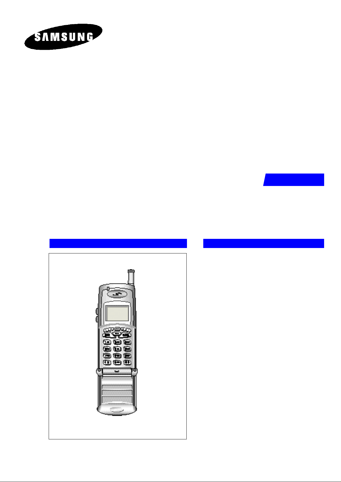
SCH-470 is composed of main handset, rapid charger, cradle, two batteries.
Samsung Electronics 1-1
General Introduction
¶UFrequency Range
Transmitter : 824.64 ~ 848.37 MHz
Receiver : 869.64 ~ 893.37 MHz
¶UChannel Spacing : 1.23 MHz
¶UNumber of Channels : 20 FA
¶UDuplex Spacing : 45 MHz
°‹MSC Transmitter Frequency
FA NO. CH. NO. CENTER FREQUENCY FA NO. CH. NO. CENTER FREQUENCY
1 1011 824.640MHz 11 404 837.120MHz
2 29 825.870MHz 12 445 838.350MHz
3 70 827.100MHz 13 486 839.580MHz
4 111 828.330MHz 14 527 840.810MHz
5 152 829.560MHz 15 568 842.040MHz
6 193 830.790MHz 16 609 843.270MHz
7 234 832.020MHz 17 650 844.270MHz
8 275 833.250MHz 18 697 845.910MHz
9 316 834.480MHz 19 738 847.140MHz
10 363 835.890MHz 20 779 848.370MHz
°‹MSC Receiver Frequency
FA NO. CH. NO. CENTER FREQUENCY FA NO. CH. NO. CENTER FREQUENCY
1 1011 869.640MHz 11 404 882.120MHz
2 29 870.870MHz 12 445 883.350MHz
3 70 872.100MHz 13 486 884.580MHz
4 111 873.330MHz 14 527 885.810MHz
5 152 874.560MHz 15 568 887.040MHz
6 193 875.790MHz 16 609 888.270MHz
7 234 877.020MHz 17 650 889.270MHz
8 275 878.250MHz 18 697 890.910MHz
9 316 879.480MHz 19 738 892.140MHz
10 363 880.890MHz 20 779 893.370MHz
1.1 General
1-2 Samsung Electronics
2. Specification
£´1.5 dBm
£ ≠104 dBm : £´18.0 dBm ~ £´30.0 dBm
Standby Output Power : below £ ≠61 dBm
Closed Loop TX Power Control Range : Test 1 beyond °æ 24 dB
Test 2 0 mS ~ 2.5 mS
Test 3 beyond °æ 24 dB
Test 4 beyond °æ 24 dB
Test 5 beyond °æ 24 dB
Size (mm) : 114 °ø50 °ø22 (Standard battery)
114 °ø50 °ø27 (Extended-life battery)
Weight (g) : 114 (Standard battery)
154 (Extended-life battery)
Samsung Electronics 2-1
Frequency Range Transmitter : 824.64 MHz ~ 848.37MHz
Frequency Range Receiver : 869.64 MHz ~ 893.37 MHz
Waveform Quality : above 0.944
Time Reference : within °æ 1uS
RX Sensitivity : £ ≠104 dBm, FER = within 0.5%
Dynamic Range : £ ≠104 dBm ~ £ ≠25 dBm, FER = within 0.5%
TX Output Power : Maximum 320 mW (25dBm)
TX Frequency Deviation : within °æ 300 Hz
Occupied Band Width : 1.32 MHz
TX Conducted Spurious Emissions : 900 kHz below £ ≠42 dBc / 30 kHz
: 1.98 MHz below £ ≠54 dBc / 30 kHz
Minimum TX Power Control : below £ ≠50 dBm
Open Loop Power Control : £ ≠25 dBm : £ ≠57.0 dBm ~ £ ≠38.5 dBm
£ ≠65 dBm : £ ≠17.5 dBm ~

2-2 Samsung Electronics
3. NAM Programming
3.1 Switching the NAM(Numeric Assignment Module) writing mode
If you performs NAM writing mode, you have to enter the password, '4, 7, *, 8, 6, 9, #, 0, 8, #, 9'.
Keypads using in NAM writing mode are as follows :
0~9 : numberic keys
¶N, # : Use to specify the variable which include several value.
VOLUME KEY : Use to switch the next item
CLR KEY : Use to retouch a wrong digit
END KEY : Use to end a NAM writing mode
: Use to store data and switching the next function
: Use to swich the last menu
Caution
-If you enter the NAM program mode, the last data displays on screen . When you need not change the
data, press VOLUME key to go to the next item.
-You can modify the data by entering a new data. And if you enter a wrong digit, press CLR to delete the
last digit.
-If you enter a wrong digit in the middle of NAM entering, continue to enter the next digits. After that
check and modify the data using volume key
- While you check the data using volume, you can store the data by pressing STO key.
- When you enter the NAM, as there are necessary information enter the phone number and LOCK code
and press STO key.
When you enter NAM programming, display following five items.
1. GENERAL ; Display the variable used commonly NAM.
2. Setup NAM 1 ; Display the variable of CDMA used commonly when you select NAM 1.
3. Setup NAM 2 ; Display the variable of CDMA used commonly when you select NAM 2.
4. Setup NAM 3 ; Display the variable of CDMA used commonly when you select NAM 3.
5. Setup NAM 4 ; Display the variable of CDMA used commonly when you select NAM 4.
If you don't store the data by pressing STO key after modifying as explains, the data does not change.
You can check the data by pressing VOLUME key without changing the data.
Samsung Electronics 3-1

NAM Programming
3-2 Setting Up NAM1
3-2-1 General
LCD Display Key in Function
4 7 * 8 6 9 # 0 8 # 9
NAM Program
1:General
2:Setup NAM1
E S N
B 0 0 0 0 0 0 0
CAI version
S C M
0 0 1 0 1 0 1 0
Lock Code
0000
47¶S869#08#9 -selects NAM programming
1 -choose 'GENERAL.'
Volume °„ Electronic Serial Number of the phone.
2
Volume °„
The version of the Common Air Interface supported by the mobile.
Volume °„ Station Class Mark displays the power class (bit 0~1),
transmission (bit2), slotted (bit5), dual mode (bit6).
(0000)
4-digit code Four-digit number supplied by the user which enables
STO electronic locking of the phone.
Slot Mode
Y e s
Slot Index
Pref NAM1...
Digital only
Pref NAM2...
Digital only
Pref NAM3...
Digital only
Pref NAM4...
Digital only
¶Sor ¶H Enables slot mode.
STO
2
0 - 7 Slot mode index.
STO Specifies the duration and frequency of times that the mobile
checks the paging channel. The higher the value, the less often the
mobile looks at the paging channel, and the more power is saved.
STO Preferred system selection for NAM1.
STO Preferred system selection for NAM2.
Up to four NAMs are allowed for the phone. This lists one of the
four NAMs.
STO Preferred system selection for NAM3.
STO Preferred system selection for NAM4.
3-2 Samsung Electronics

3-2-2 Setup NAM1
LCD Display Key in Function
NAM Programming
NAM Program
1:General
2:Setup NAM1
I M S I M C C
4 5 4
I M S I M N C
0 5
CDMA TEL NO.
8 5 2 0 0 0 0 0 0 0 0
CDMA pref...
A pref
CDMA ACCOLC
Pchn Sys A
Pchn Sys B
3 8 4
0
2 8 3
2 -choose 'NAM1.'
number International Mobile Station Identity Mobile Country Code.
STO
number International Mobile Station Identity Mobile Network Code.
STO
phone number CDMA phone number.
STO
¶Sor ¶H Preferred system selection.
STO
class number CDMA Access Overload Class.
STO This two-digit number specifies the level of priority assigned
to the mobile for accessing the system.
Ranges from 0 to 15.
channel number Primary CDMA channel for the A carrier.
STO Ranges from 0 to 1,023. 0 indicates no channel.
channel number Primary CDMA channel for the B carrier.
STO Ranges from 0 to 1,023. 0 indicates no channel.
Pchn Sys A
Schn Sys B
7 7 7
CD Acq SID 1
CD lockSID 1
CDMA HomeSID
Y e s
6 9 1
0
10640
channel number Secondary CDMA channel for the A carrier.
STO Suggested setting is 0: ranges from 0 to 1,023.
channel number Secondary CDMA channel for the B carrier.
STO Suggested setting is 0: ranges from 0 to 1,023.
ID number CDMA Acquisition System ID.
STO Enables you to set the phone to acquire up to six SIDs in the
CDMA mode. If you enter ‘0’ for any SID, the program
assumes that you have no more numbers to store.
Default setting is 0: ranges from 0 to 32,767: up to six SIDs.
ID number CDMA Lock System ID.
STO Enable you to specify up to six SIDs that the phone will be
prohibited from acquiring in CDMA mode. If all six SIDs are
set to zero, no lock restrictions will be in effect and the phone
can acquire all SIDs.
Default setting is 10640,8103,0,0,0,0 : ranges from 0 to 32,767 up
to six SIDs.
¶Sor ¶H CDMA Home System ID.
STO Enables the phone to allow mobile terminated calls while in
the home system. Controls the types of registration allowed for
the phone.
Samsung Electronics 3-3

NAM Programming
LCD Display Key in Function
CDMA fSID
CDMA fNID
SID #1
NID #1
Y e s
Y e s
1 0 6 4 1
6 5 8 3 5
¶Sor ¶H CDMA foreign System ID.
STO Enables the phone to allow mobile terminated calls while
in a foreign system. Controls the types of registration
allowed for the phone.
¶Sor ¶H CDMA foreign Network ID.
STO Enables the phone to allow mobile terminated calls while
in a foreign system and foreign network ID. Controls the
types of registration allowed for the phone.
number System Identification Number.
STO Controls how the phone acquires different systems.
Determines the roaming status for the mobile.
All SIDs range from 0 to 32,767: a 0 setting for the SID
signifies that it is not active.
number Network Identification Number.
STO Controls how the phone acquires different systems, and is
set and specified in conjunction with each SID (e.g., SID #1,
NID #1).
Determines the roaming status for the mobile.
All SIDs range from 0 to 65,535: a 0 setting for one NID
signifies that it is not active.
SID #2
NID #2
SID #3
NID #3
SID #4
NID #4
1 3
0
0
0
0
0
number See SID #1.
STO
number See NID #1.
STO
number See SID #1.
STO
number See NID #1.
STO
number See SID #1.
STO
number See NID #1.
STO
3-4 Samsung Electronics

3-3 Setting Up NAM2
LCD Display Key in Function
NAM Programming
NAM Program
1:General
2:Setup NAM1
3 -choose 'NAM2’.
The NAM2 setup program is the same as °ÆNAM1°Ø. See NAM1.
3-4 Setting Up NAM3
LCD Display Key in Function
NAM Program
3:Setup NAM2
4:Setup NAM3
4 -choose 'NAM3’.
The NAM3 setup program is the same as °ÆNAM1°Ø. See NAM1.
3-5 Setting Up NAM4
LCD Display Key in Function
NAM Program
5:Setup NAM4
5 -choose 'NAM4’.
The NAM4 setup program is the same as °ÆNAM1°Ø. See NAM1.
Samsung Electronics 3-5

NAM Programming
3-6 Samsung Electronics

4. Data Transfer
¶UData Transfer program
¶UIBM compatible PC
¶USCH-470 Test Jig
¶U3.6V Power Supply
4-2 Connection
Connect the test jig to COM1 port on the PC and
connect the interface cable of the test jig to the
phone.
Caution : When you use the Data Transfer
program with a note book PC, you might
encounter some problem. Check your serial port
setup in your notebook PC (see your note book
manual).
Don’t worry about the serial port setup when you
use a desktop PC.
4-3 Getting Started
1. Run the DTRANxx.EXE file. If you run the file
for the first time, the message 'INITIAL FILE IS
CREATED' appears. Do not delete the created
file because the file creates DTRANxx.CFG to
store environment setup data. The message
does not appear once you have run the
program.
2. Press any key to go to next procedure.
Function Keys
Fl Reads EEPROM data from the
customer's cellular phone.
F3 Displays SAMSUNG logo. To reenter
to program mode, press F3 key again.
F5 Write the data of the customer’s phone
into the EEPROM on the new board.
F8 Switches from Hands-free mode to
Diagnostic Monitor mode to allow the
data transfer. To check this mode from
the cellular phone, press FCN, 9, 1 on
the key board in sequence.
ALT+X Exits programming and returns to DOS
mode.
4-4 Operation Procedure
1. On standby mode, 'Please check the
communication link between your PC and the
phone prior to beginning ...' messages appear
on the screen. You are ready to transfer data.
2. Switch the phone power on after you have run
the program.
3. Press <F1> key to read EEPROM data from the
customer's cellular phone. On screen, 'Change
the mode of the phone from HANDS-FREE
mode to DM mode' message appears. On the
LCD display of the phone, 'AUTO TEST' and
'WRITE EEPROM' messages appear. If the
phone is already in DM(Diagnostic Monitor)
mode, the message does not appear.
4. After the mode is changed to DM, EEPROM
data on the cellular phone is read by PC. You
can monitor the reading procedure on the
screen.
5. When the data reading is completed, 'Replace
the source phone with the target phone and
press <F5> when ready' message appears on
the screen.
6. Press any key to clear the message. The cellular
phone displays 'DELETED' and '300-300-3000'
instead of greeting and phone number
respectively. All the features of the phone
including ESN are reset to default status, and
the phone can not be operated.
When the main board of a customer's cellular
phone is required to be replaced with a new one,
or the customer is needed to use a phone lent from
the service center while his phone is serviced, this
feature is used to transfer(copy) all the EEPROM
data of the customer's phone into the new board or
the lent phone to keep the information the
customer had stored into his phone personally.
4-1 Equipment Required
Samsung Electronics 4-1

Data Transfer
¶UNo way ! The test jig clears the information after
writing is done. If you force to copy it into several
units, the phone might not work properly.
¶UYou cannot perform writing procedure unless reading
is completed successfully. Error message appears on
the screen.
¶UYou can clear the error message by pressing any key.
Reading is cancelled. The EEPROM data on the phone
is not cleared. You can restart to read the data.
¶UYou can clear the error message by pressing any key.
Writing is cancelled. You can restart writing from the
beginning.
¶UIf the program halters or is interrupted for some
reasons, and you restart the program, ‘WRITING IS
BEING CARRIED OUT BY USING DATA NOT
FINISHED’ message appears on the screen. It means
that the data you have read and not wrutten is
restored and ready to write. If you have finished the
program by pressing ALT key and X without writing
after reading, the message ‘WRITING IS NOT
ACHIEVED, WILL CARRY OUT WRUTING FOR
NEXT TIME’ appears on the screen.
You tried to write EEPROM data without reading the
data first.
For some reasons, data transfer is not completed
without writing after reading the data.
Reading is interrupted in the middle of the operation
due to some problem with the phone.
Writing is interrupted in the middle of the operation
due to some problem with the phone.
¶UCheck if the serial port setup is properly made.
¶UCheck if the test jig is connected correctly. The
connection is made, by ‘1:1 PIN TO PIN’ method (not
NULL modem method). Only RX, TX signal grounds
are connected.
¶UIf you use DOS shell in Windows and COM1 is used
by another DOS shell, exit the program.
7. Remove the phone from the test jig and connect
the new phone to the test jig.
Caution: If you try to perform reading again
without writing after reading is already done once,
the error message 'READING FROM THE PHONE
WAS ALREADY BEEN CARRIED OUT,
WRITING SHOULD BE CARRIED OUT' appears
on the screen.
8. Press <F5> key to perform writing EEPROM
data. You can monitor the writing procedure
on the screen.
4-5 If Error Occurs
Symptom
Program is running, but reading is not achieved.
You tried to copy EEPROM data into several units.
9. When the data writing is completed, the phone
will reset. The program returns to standby
mode and is ready to read data from another
phone. 'WELL DONE, DATA TRANSFER IS
COMPLETED' appears on the screen.
10. Check if the transferred EEPROM data is the
same.
Solution
4-2
Samsung Electronics

5. Circuit Description
5-1 Logic Section
5-1-1 Power Supply
With the battery installed on the phone and by
pressing the END/ key, the VBATT and
ON_SW signals will be connected. This will turn
on U123 DC_DC convertor.
This in turn will be supplied to PIN3, PIN4 of
regulators U124, PIN6 of regulators U122, thus
releasing them from the shut-down state to output
regulated 3.3V. ( The VBATT applied to ON-SW
will turn on Q103(DTC144EE) resalting in the
signal ON-SW-SENSE to change start the from
High to Low.)
The MSM recognizes this signal and sends out
PS_HOLD (logical HIGH) to turn on Q102 even
after the PWR key is released.
The power from U124 is used in the digital part of
MSM and BBA. The power from U122 is used in
analog part of BBA.
5-1-2 Logic Part
The logic part consists of internal CPU of MSM,
RAM, ROM and EEPROM. The MSM receives
TCXO and CHIPX8 clock signals from the BBA
and controls the phone during the operation. The
major components are as follows:
¶UCPU : INTEL 80186 core (inside the MSM)
¶UFLASH ROM : U129 - 8 Mbit FLASH MEMORY
¶USRAM : U127 - 2 Mbit STATIC RAM
¶UFLASH ROM : U130 - 1 Mbit FLASH MEMORY
¶UEEPROM : U102 - 128 Kbit SERIAL EEPROM
CPU
INTEL 80186 CMOS type 16-bit microprocessor is
used for the main processing. The CPU controls all
the circuitry. For the CPU clock, 27MHz resonator
is used.
FLASH ROM
One 8 MBIT FROM is used to store the terminal's
program. Using the down-loading program, the
program can be changed even after the terminal is
fully assembled.
SRAM
One 2 MBIT SRAMs is used to store the internal
flag information, call processing data, and timer
data.
EEPROM
One 128 KBIT EEPROM is used to store ESN,
NAM, power level, volume level, and telephone
number.
KEYPAD
For key recognition, key matrix is setup using
SCAN0-6 of STORE signals and KEY0-3 of input
ports of MSM. Ten LEDs and backlight circuitry
are included in the keypad for easy operation in
the dark.
LCD MODULE
LCD module contains a controller which will
display the information onto the LCD by 8-bit data
from the MSM. It also consists a DC-DC converter
to supply -3.5V for fine view angle and LCD
reflector to improve the display efficiency.
Samsung Electronics 5-1

Circuit Description
5-1-3 Baseband Part
MOBILE SYSTEM MODEM (MSM)
The MSM equipped with the INTEL 80C186 CPU
core is an important component of the CDMA
cellular phone. The MSM comes in a 176 pins
TQFP package.
MICROPROCESSOR INTERFACE
The interface circuitry consists of reset circuit,
address bus (A0-A19), data bus (AD0-AD15), and
memory controls (ALE, DT_R, HWR/, LWR/,
RAM_CS/, ROM_CS).
INPUT CLOCK
¶UCPU clock: 27 MHz
¶UTXCO/4 (pin 34): 4.92 MHz. This clock signal
from the BBA is the reference clock for the MSM
except in CDMA mode.
¶UCHIPX8 : 9.8304 MHz. The reference clock used
during the CDMA mode.
BBA INTERFACE
ADC Interface
ADC_CLK (pin 3), ADC_ENABLE (pin 1) and
ADC_DATA (pin 2) are required to control the
internal ADC in the BBA.
Data Port Interface
Includes the UART. Also, supports Diagnostic
Monitor (DM), HP equipment interface, down
loading, and data service.
CODEC Interface
The MSM outputs 2.048 MHz PCM_CLK (pin 19)
and 8 KHz CODEC_SYNC (pin 16, 20) to the
CODEC (U117). The voice PCM data from the
MSM (U101) PCM_DIN (pin 135) is compressed
into 8 KHz, by QCELP algorithm in the CDMA
mode.
RF Interface
CDMA, FM Data Interface
¶UTXIQDATA0-7 (pins 24-32) : TX data bus used
during both CDMA and FM mode but it is used
only for CDMA mode at this phone.
Clock
¶UTC_CLK (pin 22), TX_CLK/(pin 23) : Analog to
Digital Converter (ADC) reference clock used in
TX mode.
¶UCHIPX8 : ADC reference clock used in CDMA
RX mode.
¶UFMCLK: TXclock used in FM mode.
TX : TX_AGC_ADJ (pin 35) port is used to control
the TX power level and PA_ON (pin 44) signal is
used to control the power amplifier. This signal
depends on the TX vocoder rate.
RX : AGC_REF (pin 36) port is used to control the
RX gain and TRK_LO_ADJ (pin 45) is used to
compensate the TCXO clock.
General Purpose I/O Register Pins
Input/output ports to control external devices.
Power Down Control
When the IDLE/ signal turns LOW, only the TX
sections will be disabled. If both the IDLE/ and
SLEEP/ change to LOW, all the pins except for the
TCXO and 27MHz clock are disabled.
5-2 Samsung Electronics

5-1-4 Audio Part
°æ2 kHz/dev.
BUZZER DRIVING CIRCUITY
Buzzer generates alert tone when the buzzer
receives the timer signal from the MSM, it
generates alert tone. The buzzer level is adjusted
by the alert signal’s period generated from the
MSM timer.
KEY TONE GENERATION
Ringer signal (pin49) out from MSM (U101) is
passed through 2 serial LPF consisting of R141,
C146, R145, and C142 amplified at the speaker
amp (U111), and comes out to speaker.
Circuit Description
Samsung Electronics 5-3
TX AUDIO PATH
The voice signal output from microphone is
filtered and amplified by the internal OP-AMP
and is converted to PCM data by the CODEC
(U117). The signal is then applied to the MSM
(U101)’s internal vocoder.
RX AUDIO PATH
The PCM data from the MSM’s converted to audio
signal by ADC of CODEC (U117), is then
amplified by the speaker amplifer (U111) to be
sent to the speaker unit.
TX WBD, ST,SAT
These signals are generated from MSM. The
modulation level of TX WBD and ST is 8
kHz/dev, and SAT is

Circuit Description
5-2 Receiver Section
LOW NOISE AMPLIFIER (LNA, Q302)
The low noise amplifier amplifies a weak signal
received from the base station to obtain the
optimum scvel (Noise figure = 1.5 dB,
Gain = 16 dB).
RADIO FREQUENCY BAND PASS FILTER
(RF BPF)
The RF BPF accepts only a specific frequency (881
°æ 12.5 MHz) from the signal received from the
base station. The band width is 25 MHz.
DOWN CONVERTER (MIXER, U302)
First local signal is applied to this down converter.
The down converter transfers the signal amplified
at the LNA into 85.38 MHz IF signal. 85.38 MHz IF
signal is made by subtracting 881 °æ12.5 MHz RF
signal from 966 °æ12.5 MHz first local signal.
IF BAND PASS FILTER (FOR CDMA)
IF SAW BPF (F303) is used for CDMA system
having 1.23 MHz wideband and °æ630 kHz
bandwidth. The filter also attenuates the image
product generated at the mixer.
BUFFER AMP (Q385)
Buffer (Q385) amplifiers signal to be applied to the
local input of the down converter (U301) when a
phase is locked between VCO (U341) and PLL IC
(U342).
AUTOMATIC GAIN CONTROLLER (AGC)
AMP U303)
85.38 MHz IF signal is applied to IF AGC amp, the
IF AGC output level is applied to BBA (Baseband
Analog ASIC). The IF AGC amp (U302) keeps the
signal at a constant level by controlling the gain.
Dynamic range is 90dB, up gain +45dB, and down
gain -45dB.
5-4 Samsung Electronics

Circuit Description
VOLTAGE CONTROLLED OSCILLATOR (VCO,
U341)
The VCO (U341) generates the signal having 966
MHz center frequency and °æ12.5 MHz deviation
with the voltage control. PLL IC (U342) controls
this signal.
ANTENNA
Antenna allows signals and send to receive from
the base station.
PHASE LOCKED LOOP (PLL, U342)
Input reference frequency is generated at
VC_TCXO (U343) and the divided signal is
generated at VCO. PLL compares the two signals
and generates the desired signal with a preprogrammed counter which controls voltage.
DUPLEXER (F301)
Duplexer (F301) controls to transmit through the
antenna only the signals within acceptable Tx
frequency range (836 °æ12.5 MHz) and to receive
through the antenna only the signals within
acceptable Rx frequency range (881 °æ12.5 MHz).
It also matches LNA input in receiving part and
PA output in transmitter part with the antenna.
POWER SUPPLY REGULATOR (U382)
The power supply regulator generates a regulated
power.
THERMISTOR (R498)
The thermistor (R498) detects temperature. It is
used to compensate active component
characteristics due to the temperature difference.
VOLTAGE CONTROLLED TEMPERATURE
COMPENSATED CRYSTAL OSCILLATOR (VCTCXO, U343)
It provides 19.68 MHz reference frequency to PLL.
A correct frequency tuning is made by the voltage
control.
Samsung Electronics 5-5

Circuit Description
5-3 Transmitter Section
BBA (U401)
BBA (U401) consists of ADC, DAC, LPF
(FM/CDMA), divider, VCO, logic control circuit,
PLL, and mixer.
BBA performs a specific function between RF part
and logic part, with MSM. The IF signal out from
Rx IF AGC amp is secondly converted throuth the
down-converter. The signal passes through the
CDMA or FM filter, converts to digital signal
through ADC, then is sent to MSM. The digital
signal out from MSM converts to analog signal
through each filter and the up-converters.
POWER AMP MODULE (U467)
Power Amp module (U467) amplifies signal (24dB
Gain) to be sent out to the base station through the
antenna.
RF BAND PASS FILTER (BPF, F451)
The RF BPF ( F451) accepts only a specific
frequency (836 °æ12.5MHz) to send it out to the
base station. The band width is 25 MHz.
POWER SUPPLY SWITCHING (U484)
Power supply switching (Q484) turns on
TX_POWER when the phone is in traffic mode and
supplies power to the circuits.
POWER SUPPLY REGULATOR (U482, U483)
The power supply regulators (U482,U483) supply
a regulated power to each part of transmitter.
U482 supplies 3.6V to TX AGC amp (U461) and
up-converter (U460). U483 supplies 3.0V to power
amp module control circuit (U487).
UP CONVERTER (MIXER, U460)
The up-converter (U460) receives the first local
signal to generate 836 °æ12.5 MHz from the BBA.
836 °æ12.5 MHz signal comes out of the mixer
output by subtracting 130 MHz IF signal from 966
°æ12.5 MHz first local signal.
RF AUTOMATIC GAIN CONTROLLER AMP
(U461, U464)
The signal out to the base station should be a
constant level. The TX RF AGC amp controls
power to keep the signal at a constant level.
5-6 Samsung Electronics
 Loading...