

Samsung S7230E Service Manual
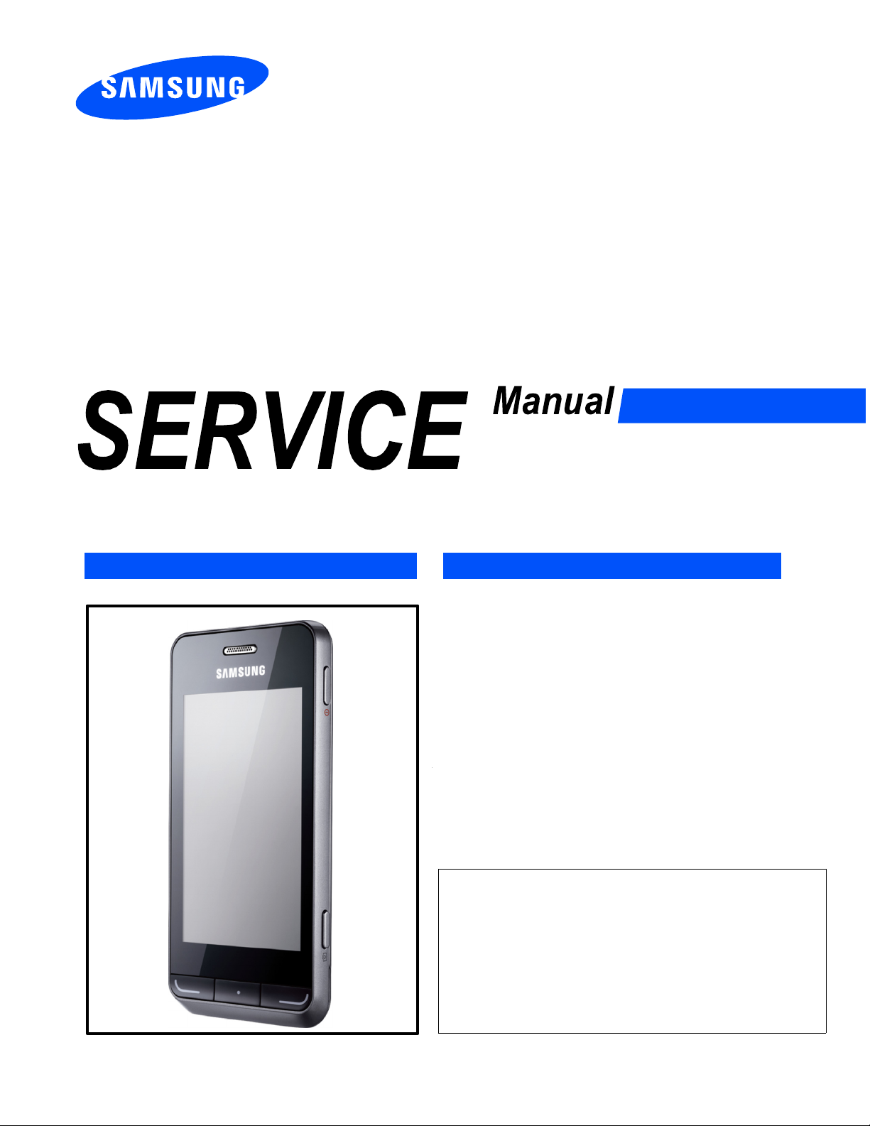
GSM TELEPHONE
GT-S7230E
efrcom
GSM TELEPHONE
CONTENTS
Safety Precautions
1.
Specification
2.
Product Function
3.
Exploded View and Parts list
4.
MAIN Electrical Parts List
5.
Level1Repair
6.
Disassembly and Assembly
7.
Instructions
Chart of Troubleshooting
8.
Reference data
9.
Notice
All functionality, features, specifications and other
product information provided in this document inclu
ding, but not limited to, the benefits, design, pricing,
components, performance, availability, and capabiliti
es of the product are subject to change without
-
notice or obligation. Samsung reserves the right to
make changes to this document and the product
described herein, at anytime, without obligation on
Samsung to provide notification of such change.
:
GSPN(Global Service Partner Network)
Country Web Site
North America service.samsungportal.com
Latin America latin.samsungportal.com
CIS cis.samsungportal.com
Europe europe.samsungportal.com
China china.samsungportal.com
Asia asia.samsungportal.com
Mideast&Africa mea.samsungportal.com
This Service Manual isaproperty of Samsung Electronics Co.,Ltd.
Any unauthorized use of Manual can be punished under applicable
International and/or domestic law.
Samsung Electronics Co.,Ltd.
ⓒ
2010. 09.
Rev.1.0
MAIN Electrical Parts List
5.
Design LOC SEC CODE Description
D401
ZD604
D300,D600
ZD401
ZD501
ZD400,ZD502,ZD503
ZD601,ZD602,ZD603
ZD606,ZD607,ZD608
ZD609,ZD700,ZD702
U502
ZD505,ZD701,ZD704
0401-001141
0403-001741
0404-001172
0406-001208
0406-001286
0406-001293
0406-001293
0406-001293
0406-001293
0406-001369
0406-001375
DIODE-SWITCHING
DIODE-ZENER
DIODE-SCHOTTKY
DIODE-TVS
DIODE-TVS
DIODE-TVS
DIODE-TVS
DIODE-TVS
DIODE-TVS
DIODE-TVS
DIODE-TVS
Q300
U303
U501
U200
UME300
PAM101
PAM100
PAM102
U408
U406
U409
U602
U400
U101
U601
U704
U202
0505-002384
0801-003016
1001-001585
1001-001607
1108-000379
1201-002967
1201-003068
1201-003088
1203-004524
1203-004807
1203-005074
1203-006025
1203-006158
1203-006159
1203-006331
1203-006456
1205-003868
FET-SILICON
IC
IC
IC
MEMORY
IC
IC
IC
IC
IC
IC
IC
IC
IC
IC
IC
IC
U201
U100
UCP300
U604
V100
R100,R101,R102,R103
1205-004099
1205-004101
1205-004105
1209-001922
1404-001221
2007-000140
5-1
SAMSUNG Proprietary-Contents may change without notice
This Document can not be used without Samsung's authorization
IC
IC
IC
IC
THERMISTOR
H
IP
R-C

Main Electrical Parts List
Design LOC SEC CODE Description
R443,R535
R104
R612
R303,R304,R311
R117,R539
R615
R315,R601,R624,R625
R710
R626
R506
R361
R517
R403
R362
R324
R363
R205,R209
R116
R124
R620
R123
R300
R206,R207,R212,R213
R214
R320
R501,R502
R323
R701,R702,R703,R704
R512,R513
R401,R402
R105,R106,R107,R108
R113
R525,R526
C168,C170,C233,C236
C336
C135,C139,C149,C153
2007-000140
2007-000142
2007-000143
2007-000144
2007-000148
2007-000156
2007-000162
2007-000162
2007-000164
2007-000165
2007-000170
2007-001319
2007-001320
2007-001339
2007-003014
2007-007021
2007-007132
2007-007480
2007-007489
2007-007798
2007-007981
2007-008045
2007-008055
2007-008055
2007-008213
2007-008294
2007-008401
2007-008531
2007-008588
2007-008780
2007-008806
2007-009257
2007-009315
2203-000233
2203-000233
2203-000254
R-CHIP
R-CHIP
R-CHIP
R-CHIP
R-CHIP
R-CHIP
R-CHIP
R-CHIP
R-CHIP
R-CHIP
R-CHIP
R-CHIP
R-CHIP
R-CHIP
R-CHIP
R-CHIP
R-CHIP
R-CHIP
R-CHIP
R-CHIP
R-CHIP
R-CHIP
R-CHIP
R-CHIP
R-CHIP
R-CHIP
R-CHIP
R-CHIP
R-CHIP
R-CHIP
R-CHIP
R-CHIP
R-CHIP
ERAMIC,CHIP
C-C
C-CERAMIC,CHIP
C-CERAMIC,CHIP
5-2
SAMSUNG Proprietary-Contents may change without notice
This Document can not be used without Samsung's authorization

Design LOC SEC CODE Description
C161,C229,C242,C309
C322,C327
C119,C125,C127,C132
C134,C202,C204,C226
C234,C235
C151,C182,C503
C114
C406,C410
C240
C106,C107,C200
C166,C239,C450,C451
C453,C608
C105
C607
C205
C504
C505,C506
C511
C169
C244
C157,C209,C213,C215
C222,C253,C337,C500
C232
C117
C104,C108,C115,C116
C162,C164
C249
C246
C123,C124
C146
C110,C111,C112,C122
C165,C167
C510
C126,C128,C129,C133
C136,C137,C138,C181
C216,C221,C247,C302
2203-000254
2203-000254
2203-000278
2203-000278
2203-000278
2203-000386
2203-000425
2203-000550
2203-000627
2203-000696
2203-000812
2203-000812
2203-000940
2203-000995
2203-001072
2203-001153
2203-001239
2203-002487
2203-002668
2203-002677
2203-002709
2203-002709
2203-005057
2203-005234
2203-005281
2203-005281
2203-005395
2203-005450
2203-005682
2203-005729
2203-005734
2203-005792
2203-005968
2203-006048
2203-006048
2203-006048
Main Electrical Parts List
C-CERAMIC,CHIP
C-CERAMIC,CHIP
C-CERAMIC,CHIP
C-CERAMIC,CHIP
C-CERAMIC,CHIP
C-CERAMIC,CHIP
C-CERAMIC,CHIP
C-CERAMIC,CHIP
C-CERAMIC,CHIP
C-CERAMIC,CHIP
C-CERAMIC,CHIP
C-CERAMIC,CHIP
C-CERAMIC,CHIP
C-CERAMIC,CHIP
C-CERAMIC,CHIP
C-CERAMIC,CHIP
C-CERAMIC,CHIP
C-CERAMIC,CHIP
C-CERAMIC,CHIP
C-CERAMIC,CHIP
C-CERAMIC,CHIP
C-CERAMIC,CHIP
C-CERAMIC,CHIP
C-CERAMIC,CHIP
C-CERAMIC,CHIP
C-CERAMIC,CHIP
C-CERAMIC,CHIP
C-CERAMIC,CHIP
C-CERAMIC,CHIP
C-CERAMIC,CHIP
C-CERAMIC,CHIP
C-CERAMIC,CHIP
C-CERAMIC,CHIP
ERAMIC,CHIP
C-C
C-CERAMIC,CHIP
C-CERAMIC,CHIP
5-3
SAMSUNG Proprietary-Contents may change without notice
This Document can not be used without Samsung's authorization

Main Electrical Parts List
Design LOC SEC CODE Description
C304,C306,C308,C311
C314,C315,C319,C321
C323,C325,C326,C339
C419,C421,C452,C533
C534,C616
C237
C701
C702
C224,C225,C248,C522
C523
C201,C203,C207
C454
C400,C527
C140,C141,C142,C143
C301,C303,C307,C313
C316,C318,C320,C324
C328,C409,C420,C423
C424,C427,C428,C429
C430,C431,C434,C435
C437,C438,C439,C440
C441,C457,C463,C465
C468,C475,C535,C624
C626,C628
C154,C155
C113
C413,C417,C464,C509
C120
C148,C211,C403,C609
C610
C411,C412
C158,C159,C160,C163
C208,C210,C214,C217
C218,C219,C220,C227
C228,C238,C241,C425
C426,C432,C433,C436
C147,C415,C416,C519
2203-006048
2203-006048
2203-006048
2203-006048
2203-006048
2203-006123
2203-006190
2203-006257
2203-006260
2203-006260
2203-006305
2203-006324
2203-006348
2203-006399
2203-006399
2203-006399
2203-006399
2203-006399
2203-006399
2203-006399
2203-006399
2203-006399
2203-006399
2203-006410
2203-006426
2203-006562
2203-006642
2203-006824
2203-006824
2203-006844
2203-006846
2203-006872
2203-006872
2203-006872
2203-006872
2203-006890
C-CERAMIC,CHIP
C-CERAMIC,CHIP
C-CERAMIC,CHIP
C-CERAMIC,CHIP
C-CERAMIC,CHIP
C-CERAMIC,CHIP
C-CERAMIC,CHIP
C-CERAMIC,CHIP
C-CERAMIC,CHIP
C-CERAMIC,CHIP
C-CERAMIC,CHIP
C-CERAMIC,CHIP
C-CERAMIC,CHIP
C-CERAMIC,CHIP
C-CERAMIC,CHIP
C-CERAMIC,CHIP
C-CERAMIC,CHIP
C-CERAMIC,CHIP
C-CERAMIC,CHIP
C-CERAMIC,CHIP
C-CERAMIC,CHIP
C-CERAMIC,CHIP
C-CERAMIC,CHIP
C-CERAMIC,CHIP
C-CERAMIC,CHIP
C-CERAMIC,CHIP
C-CERAMIC,CHIP
C-CERAMIC,CHIP
C-CERAMIC,CHIP
C-CERAMIC,CHIP
C-CERAMIC,CHIP
C-CERAMIC,CHIP
C-CERAMIC,CHIP
ERAMIC,CHIP
C-C
C-CERAMIC,CHIP
C-CERAMIC,CHIP
5-4
SAMSUNG Proprietary-Contents may change without notice
This Document can not be used without Samsung's authorization
Design LOC SEC CODE Description
C109,C121
C103,C402,C531,C604
C606
C212,C230,C617,C622
C633
C223,C231,C455
C602
C405
L208
L211
L102
L105
L200
L120
L100,L101,L112,L113
L504
L118
L107
L115,L116
2203-007271
2203-007279
2203-007279
2203-007317
2203-007317
2203-007393
2203-007687
2404-001506
2703-001701
2703-001728
2703-001749
2703-001751
2703-001786
2703-001868
2703-002176
2703-002231
2703-002267
2703-002593
2703-002793
Main Electrical Parts List
C-CERAMIC,CHIP
C-CERAMIC,CHIP
C-CERAMIC,CHIP
C-CERAMIC,CHIP
C-CERAMIC,CHIP
C-CERAMIC,CHIP
C-CERAMIC,CHIP
C-TA,CHIP
INDUCTOR
INDUCTOR
INDUCTOR
INDUCTOR
INDUCTOR
INDUCTOR
INDUCTOR
INDUCTOR
INDUCTOR
INDUCTOR
INDUCTOR
L117
L119
L601
L600
L114,L404
L400,L401
L206
OSC400
OSC200
TCX200
TCX100
F600,F601
F605
F603,F604
F201
F104
F100
2703-002953
2703-002999
2703-003347
2703-003485
2703-003685
2703-003686
2703-003698
2801-004373
2801-004589
2809-001348
2809-001351
2901-001462
2901-001463
2901-001470
2904-001759
2904-001789
2904-001868
INDUCTOR
INDUCTOR
INDUCTOR
INDUCTOR
INDUCTOR
INDUCTOR
INDUCTOR
CRYSTAL-UNIT
CRYSTAL-UNIT
OSCILLATOR-VCTCXO
OSCILLATOR-VCTCXO
FILTER-EMI
FILTER-EMI
FILTER-EMI
ER-SAW
FILT
FILTER-SAW
FILTER-SAW
5-5
SAMSUNG Proprietary-Contents may change without notice
This Document can not be used without Samsung's authorization
Main Electrical Parts List
Design LOC SEC CODE Description
F101
F200
F103
F102
MIC500
L207
L201,L202
L501,L502
L203,L204,L205
2904-001869
2909-001299
2910-000062
2910-000092
3003-001136
3301-001438
3301-001534
3301-001812
3301-001820
FILTER-SAW
FILTER-DUPLEXER
FILTER
FILTER
MIC
CORE-FERRITE BEAD
CORE-FERRITE BEAD
CORE-FERRITE BEAD
CORE-FERRITE BEAD
L500,L509,L510,L513
L505,L511
CN100
HDC600
HDC401,HDC500
HEA600
HDC400
BTC600
ANT103
ANT100,ANT101,ANT200
ANT201
IFC500
BT_ANT
3301-001885
3301-001986
3705-001731
3708-002162
3710-002632
3711-006101
3711-006923
3711-007312
3712-001348
3712-001361
3712-001361
3722-003065
4202-001524
CORE-FERRITE BEAD
CORE-FERRITE BEAD
CONNECTOR-COAXIAL
CONNECTOR
CONNECTOR-SOCKET
CONNECTOR-HEADER
CONNECTOR-HEADER
CONNECTOR-HEADER
CONNECTOR
CONNECTOR
CONNECTOR
JACK-PHONE
LDA212G6910F-293
LED600 GH59-08444A CHP-C4040-200-PB2016
SC101,SC102,SC103 GH70-04443A ONBOARD-CLIP
SC104,SC105,SC106 GH70-04443A ONBOARD-CLIP
SC107,SC108 GH70-04443A ONBOARD-CLIP
Please consult the GSPN website(Samsung Portal) for the most recent version of the product's
part list.
5-6
SAMSUNG Proprietary-Contents may change without notice
This Document can not be used without Samsung's authorization
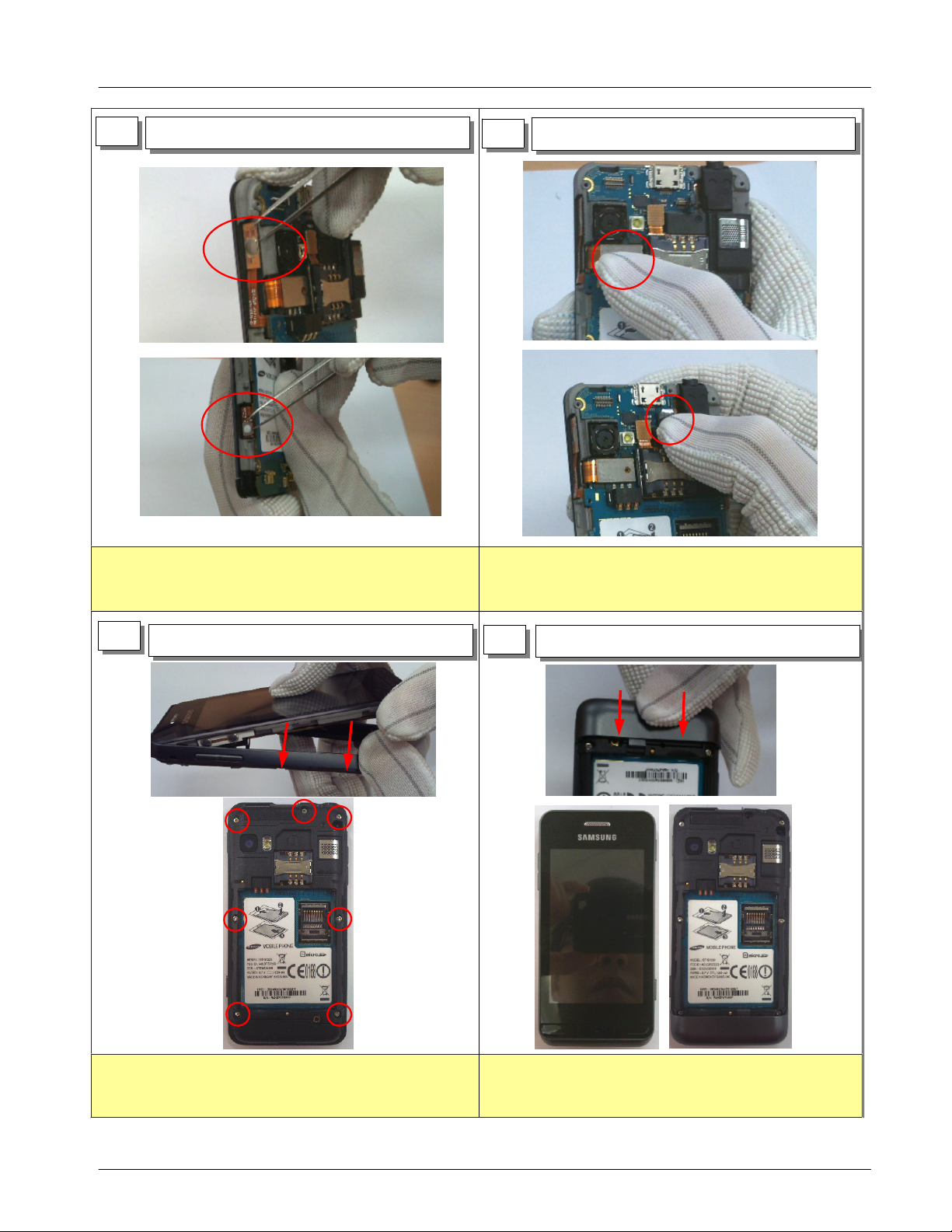
Level
7.
Disassembly and Assembly Instructions
7-1.
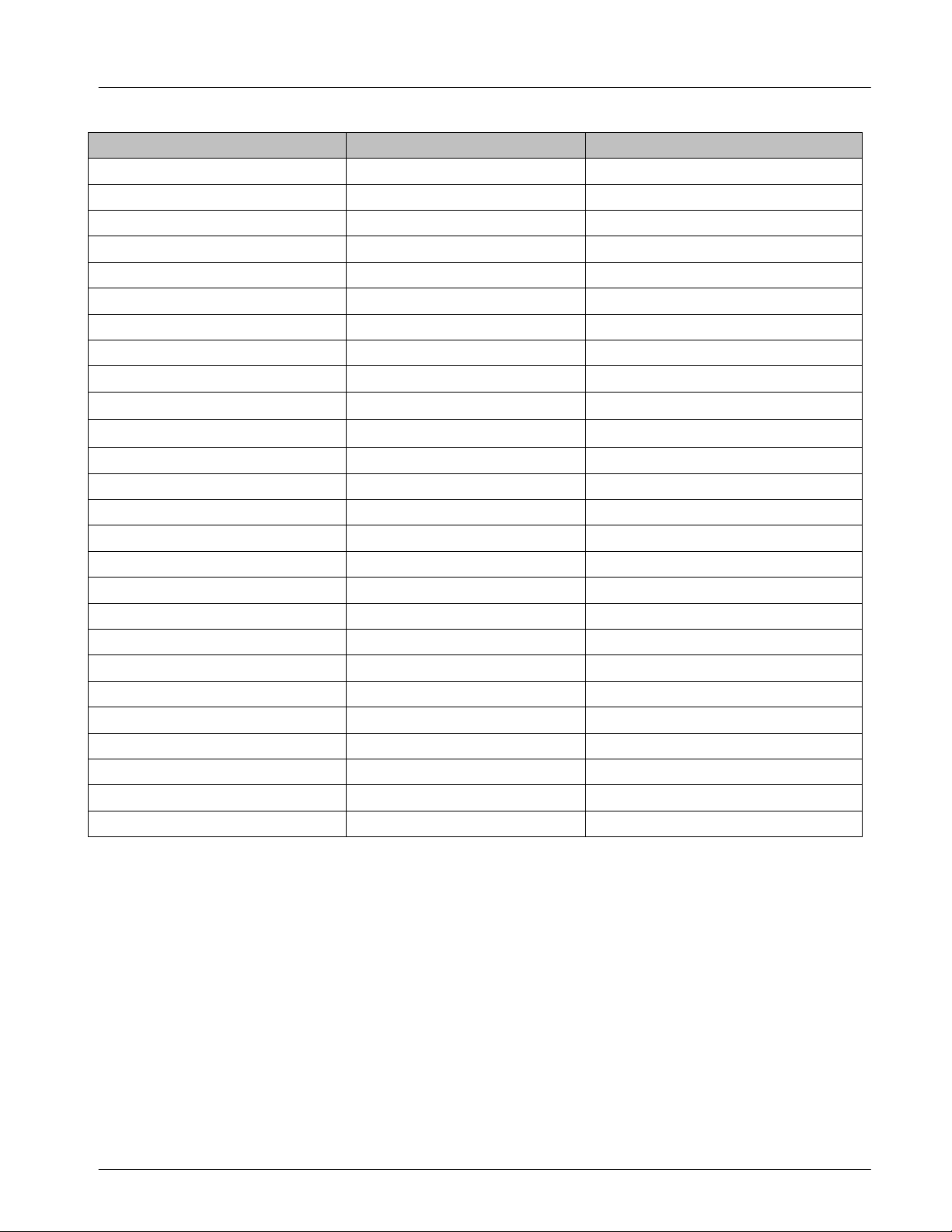
Repair
2
7-1-1.
1)
Disassembly
1 2
Be careful not to make scratch and molding damage!
Disassemble RF COVER at REAR
Release Screw7Point at REAR
Be careful not to make scratch and molding damage!
1)
3
Disassemble FRONT from REAR
Lift FRONT upward.
1)
Detach Side key FPCB.
4
Detach Power Key FPCB and Cammera Key FPCB.
1)
Be careful not to damage to FPCB(Use tweezer!)
2)
7-1
SAMSUNG Proprietary-Contents may change without notice
This Document can not be used without Samsung's authorization
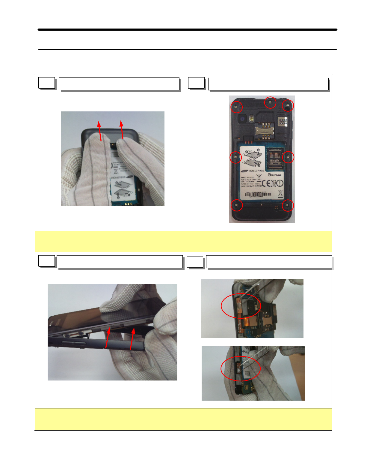
Level2Repair
7.
5
Disassemble FPCB.
6
Disassemble Main PBA from the FRONT Ass'y
Detach LCD FPCB.
1)
Detach Earjack FPCB.
2)
7
Disassemble Module from PBA.
Hold up Main PBA from left.
1)
Detach T-flash FPCB.
2)
8
Complete disassembly.
Disassemble SPK Module from PBA.
1)
Disassemble Cammera Module from PBA
2)
SAMSUNG Proprietary-Contents may change without notice
This Document can not be used without Samsung's authorization
7-2
Level2Repair
7.
7-1-1.
1
Assembly
SetaPBA and FRONT Ass'y.
2
Assemble Camera module and SPK module.
3
Assemble T-Flash FPCB.
Assemble Camera module on PBA.
1)
Assemble SPK module and FPCB on PBA
2)
4
Assemble PBA on FRONT Ass'y.
Be careful not to make damage to FPCB
1)
SAMSUNG Proprietary-Contents may change without notice
This Document can not be used without Samsung's authorization
1)
7-3
Level2Repair
7.
5
Assemble PBA on FRONT Ass'y.
6
Assemble PBA on FRONT Ass'y.
Assemble Power Key FPCB and Cammera Key FPCB.
1)
Be careful not to damage to FPCB.
2)
7
Assemble FRONT Ass'y on REAR.
Assemble LCD FPCB on PBA.
1)
Assemble Earjack FPCB FPCB on PBA.
1)
8
Assemble RF Cover, and complete assembly
Be careful not to make scratch and molding damage!
1)
2) Drive Screws at 6 points with torque 1.1 +/- 0.1 Kgf/ɜ.
SAMSUNG Proprietary-Contents may change without notice
This Document can not be used without Samsung's authorization
Be careful not to make scratch and molding damage!
1)
7-4
Level
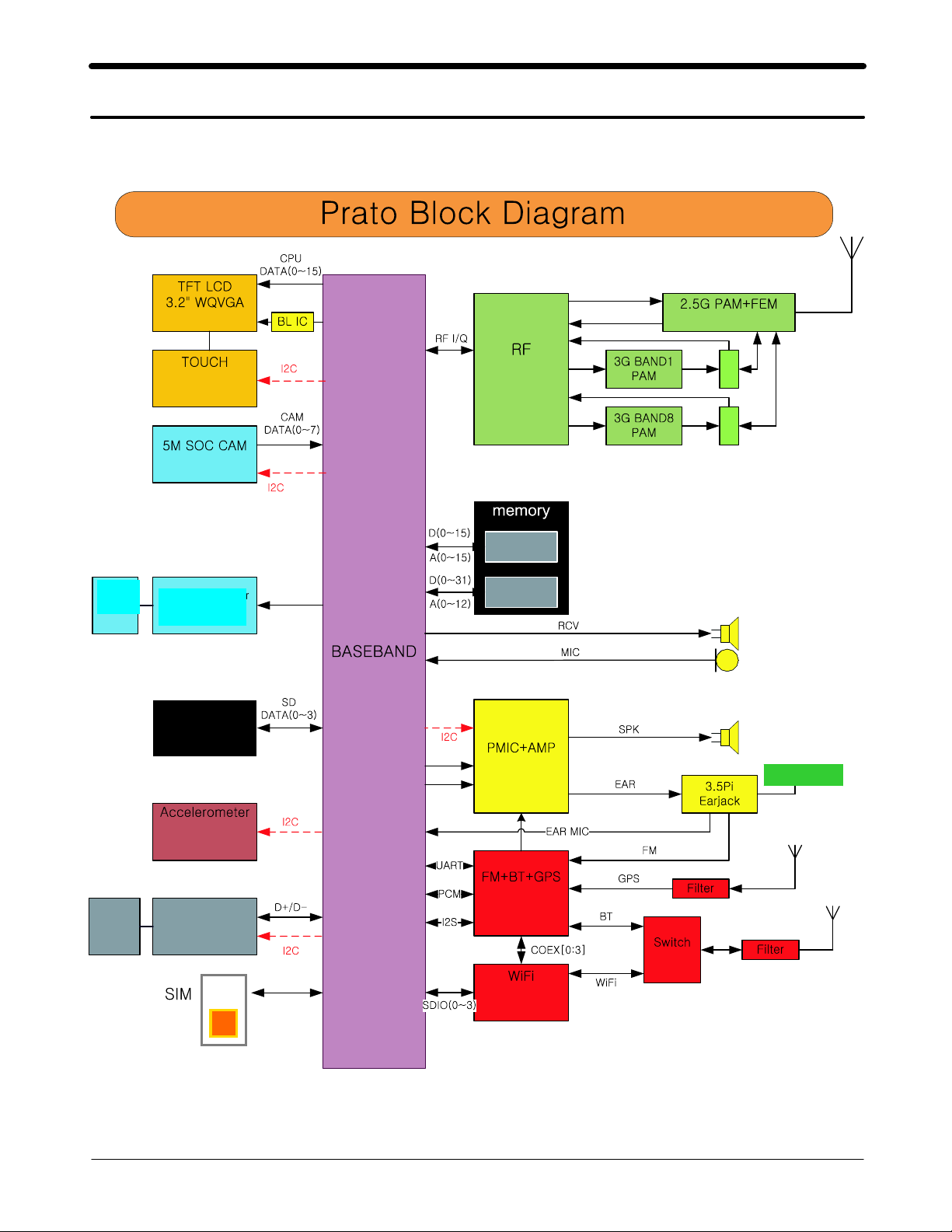
8.
Block Diagram
8-1.
Repair
3
4Gb
oneNAND
Flash
LED
u-USB
IF
Flash LED
Driver
SD CARD
USB
Switch
2Gb SDR
SDRAM
EARPHONE
8-1
SAMSUNG Proprietary-Contents may change without notice
This Document can not be used without Samsung's authorization
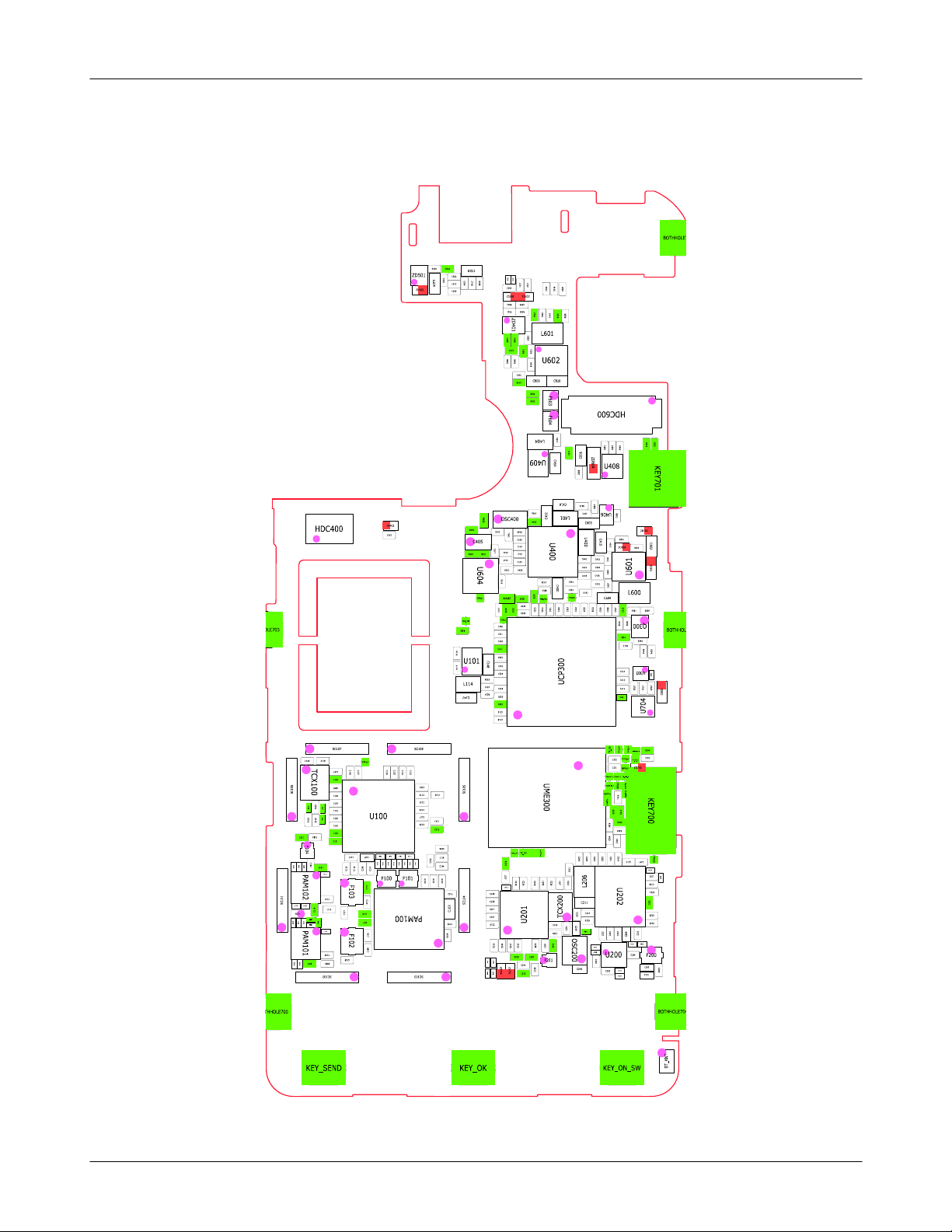
Level3Repair
PCB Diagrams
8-2.
8-2-1.
Top
8-2
SAMSUNG Proprietary-Contents may change without notice
This Document can not be used without Samsung's authorization
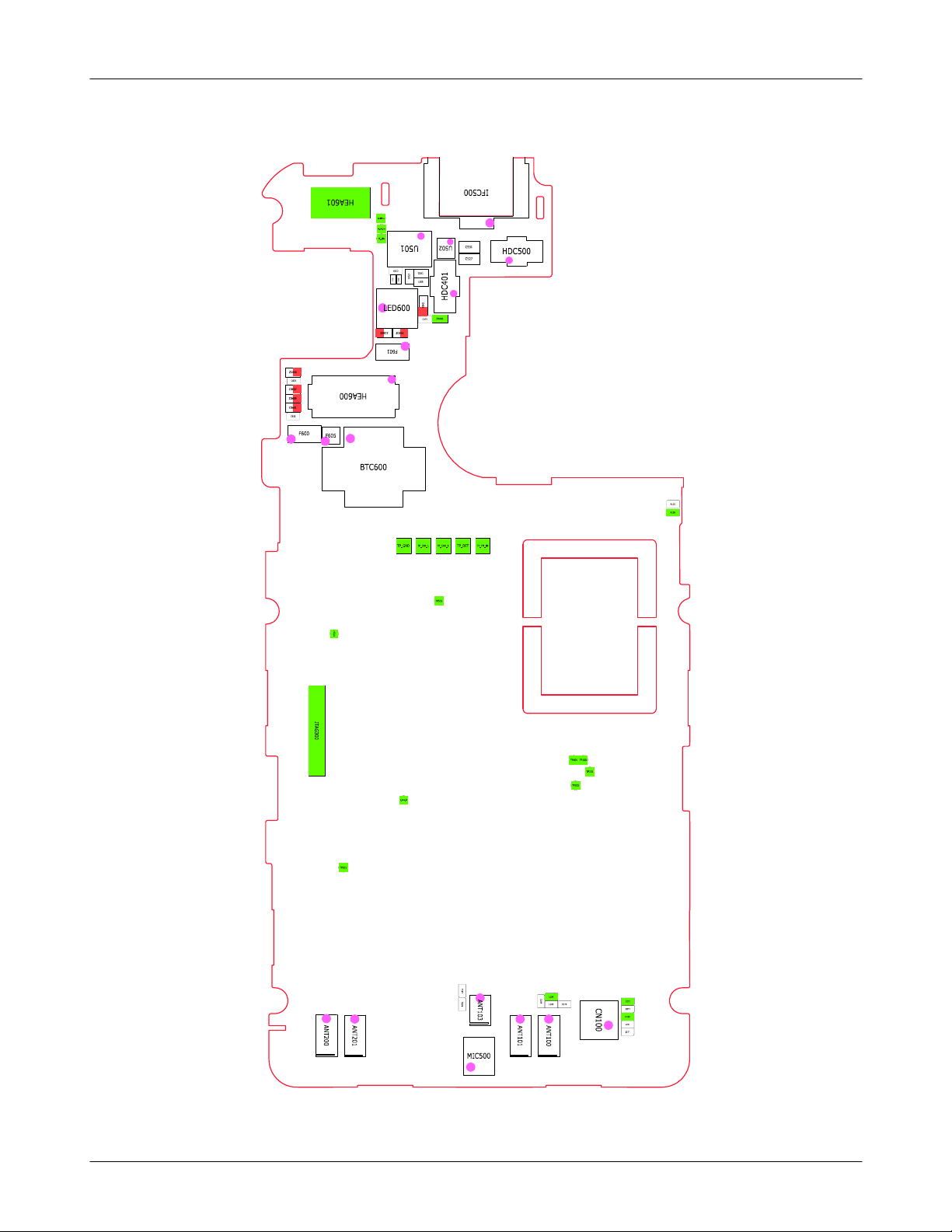
Level3Repair
8-2-2.
Bottom
8-3
SAMSUNG Proprietary-Contents may change without notice
This Document can not be used without Samsung's authorization
Level3Repair
8-3-1.
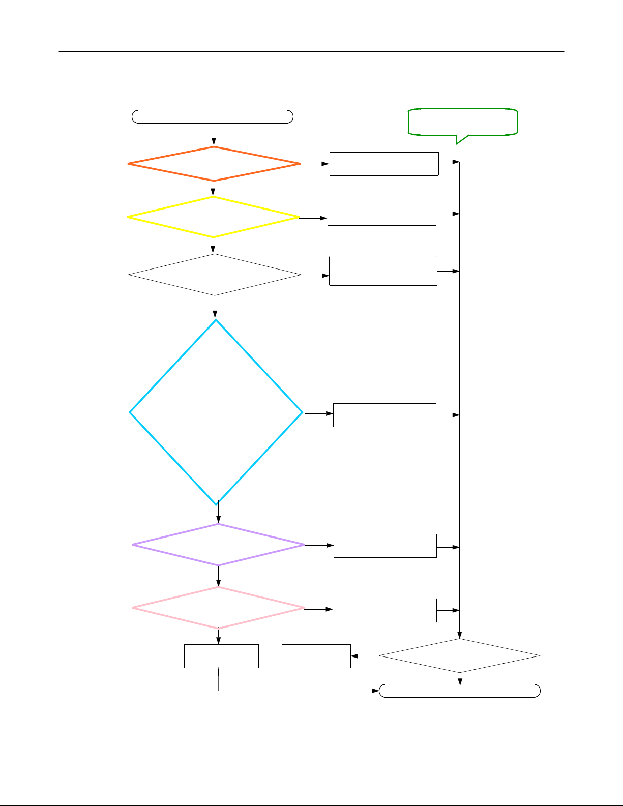
Power On
Power On"does not work
"
Check theVBAT Voltage
C606 or C608
@
Is the soldered status of
KEY701(ON KEY) O.K?
Current consumption
>= 100mA?
Check the power
VAMP1_3.0V(C436)
VANLG1_3.0V(C441)
VDD_1.2V(C426)
VUSB_3.3V_NVM(C434)
VDDORF2_2.5V(C432)
VCORE_1.2V(C415)
VBBD_2.9V(C440)
VMEM_1.8V(C416)
VSIM_3.0V(C424)
VDDAUX1_2.9V(C439)
VANLG2_3.0V(C430)
>=3.3V
YES
YES
YES
NO
NO
NO
Charge the Battery
1.
V, put more lead
2.If0
C606, C608
@
Put more lead each terminal
1.
Replace KEY701
2.
Download binary again
NO
power management problem.
Put more lead solder
each terminal
.
If you
do
#2!!!
try and fail,
#1
YES
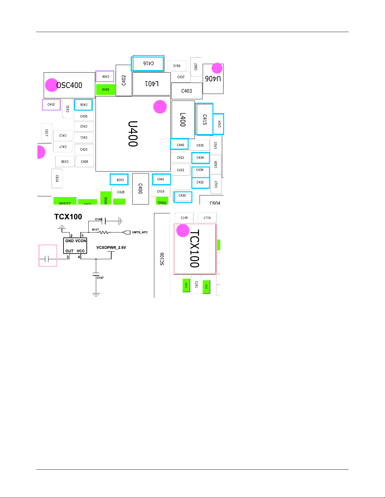
Check the OSC400
C406,410)=
(
Check the TCX100
Replace Board(PBA)
32.768
C153=26MHz
@
YES
YES
KHz
?
NO
?
NO
Back to
previous step
inner clock problem.
Put more lead solder
each terminal
Put more lead soler
each terminal
NO
Is It power turned on?
8-4
SAMSUNG Proprietary-Contents may change without notice
This Document can not be used without Samsung's authorization
YES
END
Level3Repair
8-5
SAMSUNG Proprietary-Contents may change without notice
This Document can not be used without Samsung's authorization
Level3Repair
C153
8-6
SAMSUNG Proprietary-Contents may change without notice
This Document can not be used without Samsung's authorization
Level3Repair
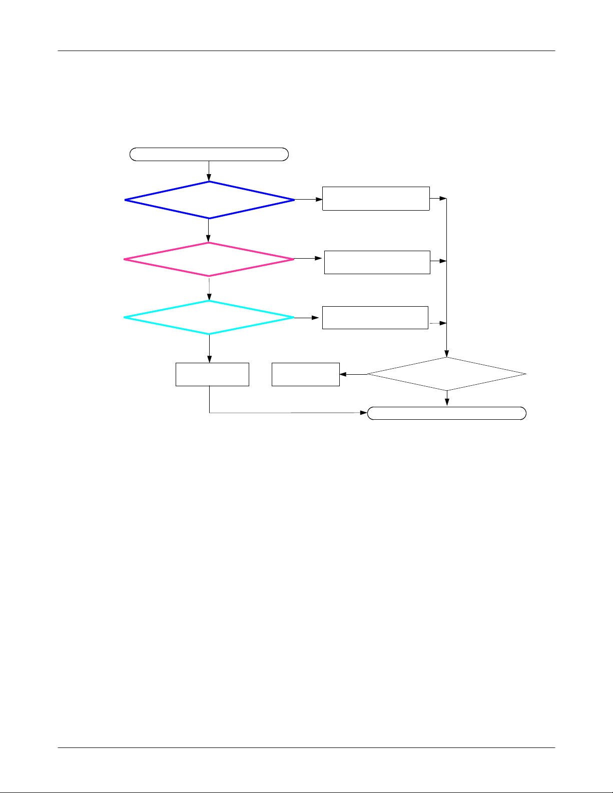
8-3-2.
SIM part
"
Insert SIM card" is displayed on the LCD
Check the connection of
HDC401 to SIM card
YES
Check the connection
C450,C451,C453
YES
Check the voltage
C452
@
Replace Board(PBA)
=3.0V?
YES
NO
NO
NO
Back to
previous step
insert SIM card again
after check connection HDC401
Put more lead each terminal
Put more lead each terminal
Does Phone accept
NO
the SIM card?
YES
END
8-7
SAMSUNG Proprietary-Contents may change without notice
This Document can not be used without Samsung's authorization
 Loading...