

Samsung S6C0672 Datasheet

S6C0672
written permission of LCD Driver IC Team.
6 BIT 384 CHANNEL TFT-LCD SOURCE DRIVER
Contents in this document are subject to change without notice. No part of this document may be reproduced
or transmitted in any form or by any means, electronic or mechanical, for any purpose, without the express
August. 1999.
Ver. 0.0
Prepared by: Myoung-Sik, Suh
mail to: mssuh@samsung.co.kr

S6C0672 6 BIT 384 CHANNEL TFT-LCD SOURCE DRIVER
S6C0672 Specification Revision History
Version Content Date
0.0 Original Aug.1999
2

6 BIT 384 CHANNEL TFT-LCD SOURCE DRIVER S6C0672
CONTENTS
INTRODUCTION..................................................................................................................................................4
FEATURES .........................................................................................................................................................4
BLOCK DIAGRAM..............................................................................................................................................5
PIN ASSIGNMENTS............................................................................................................................................6
PIN DESCRIPTIONS ...........................................................................................................................................7
OPERATION DESCRIPTION...............................................................................................................................8
DISPLAY DATA TRANSFER............................................................................................................................8
EXTENSION OF OUTPUT................................................................................................................................8
RELATIONSHIP BETWEEN INPUT DATA VALUE AND OUTPUT VOLTAGE ..................................................8
ABSOLUTE MAXIMUM RATINGS.....................................................................................................................15
RECOMMENDED OPERATION CONDITIONS .................................................................................................. 15
DC CHARACTERISTICS................................................................................................................................... 16
AC CHARACTERISTICS................................................................................................................................... 17
WAVEFORMS................................................................................................................................................... 18
RELATIONSHIPS BETWEEN CLK1, START PULSE (DIO1, DIO2) AND BLANKING PERIOD........................19
3

S6C0672 6 BIT 384 CHANNEL TFT-LCD SOURCE DRIVER
INTRODUCTION
The S6C0672 is a 384 channel output, TFT-LCD source driver for 64 gray scale displays. Data input is based on
digital input consisting of 6 bits by 6 dots, which can realize a full-color display of 260,000 colors by output of 64
values gamma-corrected.
This device has an internal D/A (Digital-to-Analog) converter for each output and 10 (5-by-2) external power
supplies. Because the output dynamic range is as large as 6.6 - 12.6 Vp-p, it is unnecessary to operate level
inversion of the LCD's common electrode. Besides, to be able to deal with dot-line inversion when mounted on a
single-side, output gray scale voltages with different polarity can be output to the odd number output pins and the
even output pins.
S6C0672 can be adopted to larger panel, and SHL (Shift Direction Selection) pin makes use of the LCD panel
connection conveniently. Maximum operation clock frequency is 65 MHz at a 2.7 V logic operation. It can be
applied to the TFT-LCD panel of XGA, SXGA standards.
FEATURES
• TFT active matrix LCD source driver LSI
• 64 gray scale is possible through 10 (5 by 2) external power supply and D/A converter
• Both dot inversion display and N-line inversion display are possible
• CMOS level input
• Compatible with gamma-correction
• Input data inversion function (DATPOL)
• Logic supply voltage: 2.7 - 3.6 V
• LCD driver supply voltage: 7.0 - 13.0 V
• Output dynamic range: 6.6 - 12.6 Vp-p
• Maximum operating frequency: fMAX = 65 MHz (internal data transmission rate at 2.7 V operation)
• Output: 384 outputs
• TCP available
4
6 BIT 384 CHANNEL TFT-LCD SOURCE DRIVER S6C0672
Y001
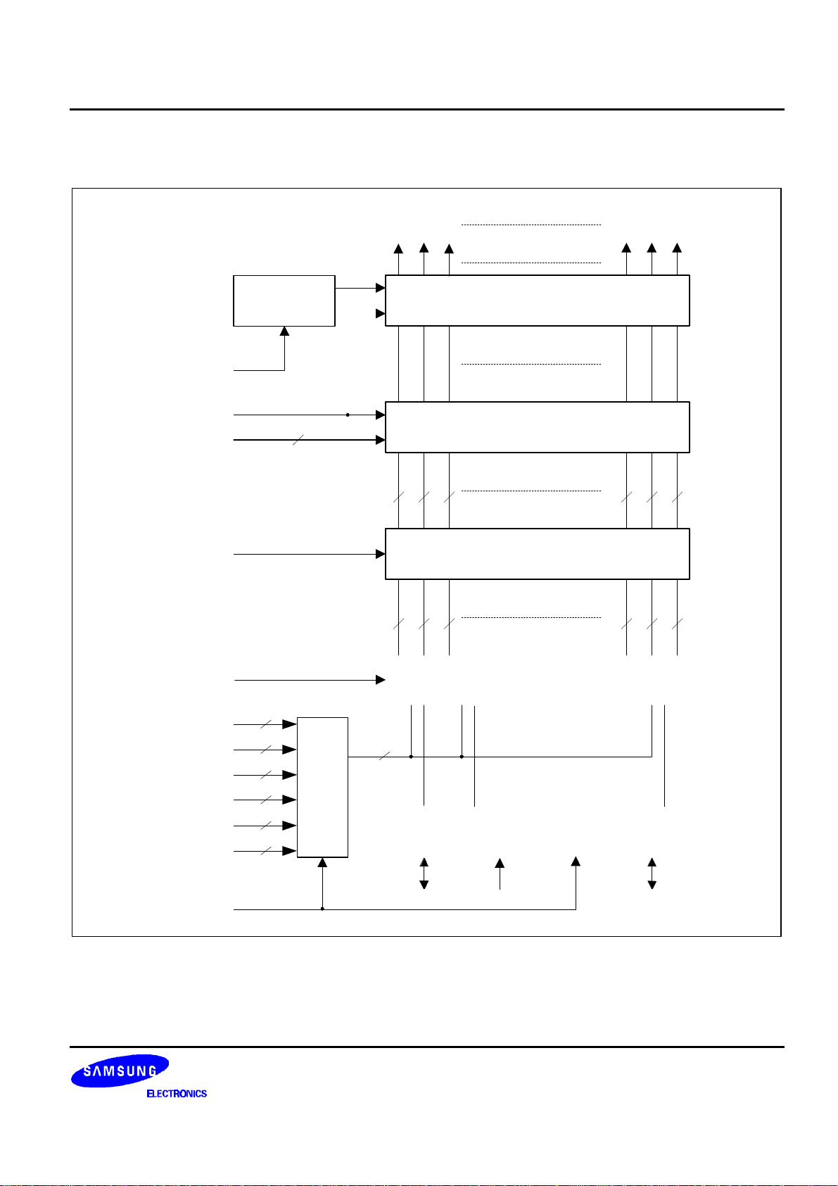
BLOCK DIAGRAM
TEST
POL
VGMA1 VGMA10
CLK1
BIAS
10
Y384
6 6 6 6 6 6
6 6 6 6 6 6
Y383
Y382
Output Buffer
D/A Converter
Data Latch
Y003
Y002
DATPOL
D00 - D05
D10 - D15
D20 - D25
D30 - D35
D40 - D45
D50 - D55
CLK2
Data Register
6
6
6
6
6
6
36
Data Control
DIO2
64bit Shift Register
SHL
DIO1
Figure 1. S6C0672 Block Diagram
5
S6C0672 6 BIT 384 CHANNEL TFT-LCD SOURCE DRIVER
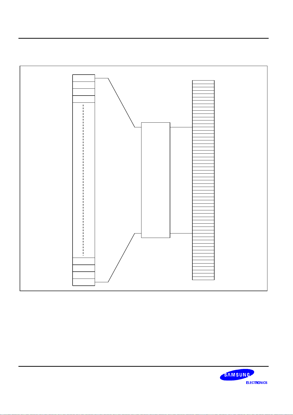
PIN ASSIGNMENTS
Y001
Y002
Y003
Y004
Y381
Y382
Y383
Y384
(Top View)
S6C0672
VSS2
VSS2
VDD2
VDD2
TEST
TEST
D00
D00
D01
D01
D02
D02
D03
D03
D04
D04
D05
D05
D10
D10
D11
D11
D12
D12
D13
D13
D14
D14
D15
D15
D20
D20
D21
D21
D22
D22
D23
D23
D24
D24
D25
D25
DIO1
DIO1
DATPOL
DATPOL
VSS1
VSS1
CLK2
CLK2
VDD1
VDD1
VGMA1
VGMA1
VGMA2
VGMA2
VGMA3
VGMA3
VGMA4
VGMA4
VGMA5
VGMA5
VGMA6
VGMA6
VGMA7
VGMA7
VGMA8
VGMA8
VGMA9
VGMA9
VGMA10
VGMA10
DIO2
DIO2
D30
D30
D31
D31
D32
D32
D33
D33
D34
D34
D35
D35
D40
D40
D41
D41
D42
D42
D43
D43
D44
D44
D45
D45
D50
D50
D51
D51
D52
D52
D53
D53
D54
D54
D55
D55
CLK1
CLK1
POL
POL
SHL
SHL
VDD2
VDD2
VSS2
VSS2
Figure 2. S6C0672 Pin Assignments
6
 Loading...