

Samsung S6C0641 Datasheet

6 BIT 300 / 309 CHANNEL TFT-LCD SOURCE DRIVER
S6C0641
written permission of LCD Driver IC Team.
November. 1999.
Prepared by: Sangho Park
mrno1@samsung.co.kr
Ver. 0.1
Contents in this document are subject to change without notice. No part of this document may be reproduced
or transmitted in any form or by any means, electronic or mechanical, for any purpose, without the express

S6C0641 6 BIT 300 / 309 CHANNEL TFT-LCD SOURCE DRIVER
S6C0641 Specification Revision History
Version Content Date
0.0 Original Aug.1999
0.1 The content of page 21 has been modified Nov.1999
2

6 BIT 300 / 309 CHANNEL TFT-LCD SOURCE DRIVER S6C0641
CONTENTS
INTRODUCTION .................................................................................................................................................4
FEATURES.........................................................................................................................................................4
BLOCK DIAGRAM..............................................................................................................................................5
PIN ASSINGMENTS............................................................................................................................................ 6
PIN DESCRIPTIONS...........................................................................................................................................7
OPERATION DESCRIPTION...............................................................................................................................8
DISPLAY DATA TRANSFER............................................................................................................................8
EXTENSION OF OUTPUT ...............................................................................................................................8
RELATIONSHIP BETWEEN INPUT DATA VALUE AND OUTPUT VOLTAGE..................................................9
ABSOLUTE MAXIMUM RATINGS ....................................................................................................................18
RECOMMENDED OPERATION CONDITIONS.................................................................................................. 18
DC CHARACTERISTICS ................................................................................................................................... 19
AC CHARACTERISTICS ................................................................................................................................... 20
WAVEFORMS...................................................................................................................................................21
RELATIONSHIPS BETWEEN CLK1, START PULSE (DIO1, DIO2) AND BLANKING PERIOD........................22
3

S6C0641 6 BIT 300 / 309 CHANNEL TFT-LCD SOURCE DRIVER
INTRODUCTION
The S6C0641 is a 300 channel or 309 channel output, TFT-LCD source driver for 64 gray scale displays. Data
input is based on digital input consisting of 6 bits by 3 dots, which can realize a full-color display of 260,000 colors
by output of 64 values gamma-corrected.
This device has an internal D/A (Digital-to-Analog) converter for each output and 9 or 11 external power supplies.
S6C0641 can be adopted to larger panel, and SHL (Shift Direction Selection) pin makes use of the LCD panel
connection conveniently. Maximum operation clock frequency is 55 MHz at a 3.3 V logic operation. It can be
applied to the TFT-LCD panel of SVGA, XGA standards.
FEATURES
• TFT active matrix LCD source driver LSI
• 64 gray scale is possible through 9 or 11 external power supply and D/A converter
• Line inversion display is possible
• CMOS level input
• Compatible with gamma-correction
• Logic supply voltage: 3.0 - 5.5 V
• LCD driver supply voltage: 3.0 - 5.5 V
• Output dynamic range: 2.6 - 5.1 Vp-p
• Maximum operating frequency: fMAX = 55 MHz (internal data transmission rate at 3.3 V operation)
• Output: 300 / 309 outputs
• TCP available
4
6 BIT 300 / 309 CHANNEL TFT-LCD SOURCE DRIVER S6C0641
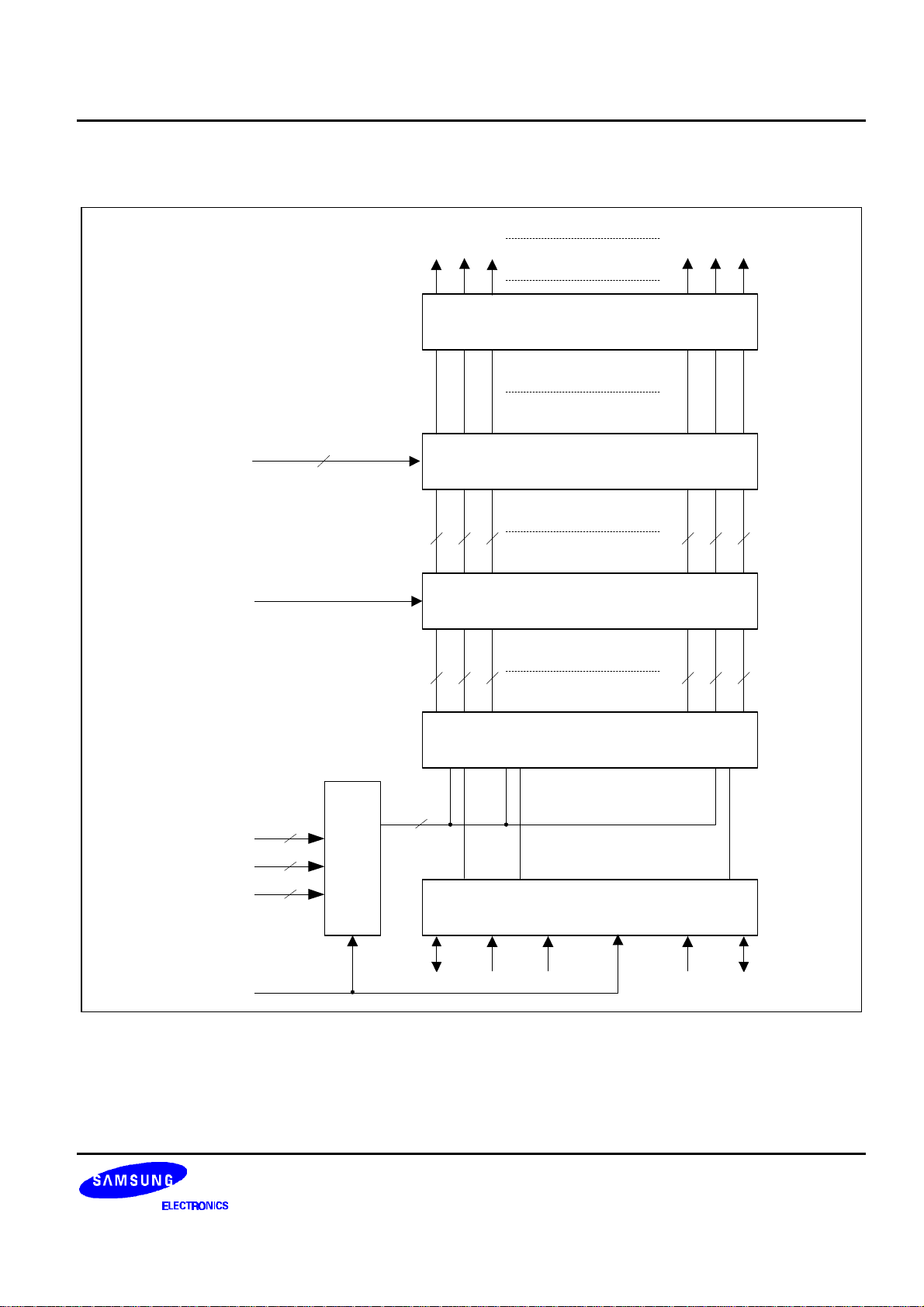
BLOCK DIAGRAM
VGMA1 VGMA11
CLK1
11
Y309
6 6 6 6 6 6
6 6 6 6 6 6
Y308
Y307
Output Buffer
D/A Converter
Data Latch
Y003
Y002
Y001
D00 - D05
D10 - D15
D20 - D25
CLK2
Data Register
18
6
6
6
Data Control
DIO2 DIO1
100 / 103 bit Shift Register
SELT
SHL TESTB
Figure 1. S6C0641 Block Diagram
5

S6C0641 6 BIT 300 / 309 CHANNEL TFT-LCD SOURCE DRIVER
PIN ASSIGNMENTS
Y001
Y002
Y003
Y004
VSS2
VDD2
VGMA10
VGMA8
VGMA6
VGMA4
VGMA2
D05
D04
D03
D02
D01
D00
D15
D14
D13
D12
D11
D10
DIO1
VSS1
SELT
CLK2
VDD1
(Top View)
S6C0641
DIO2
CLK1
D25
D24
D23
D22
D21
D20
SHL
VGMA1
VGMA3
VGMA5
VGMA7
VGMA9
VGMA11
VDD2
VSS2
Y306
Y307
Y308
Y309
Figure 2. S6C0641 Pin Assignments
6

6 BIT 300 / 309 CHANNEL TFT-LCD SOURCE DRIVER S6C0641
PIN DESCRIPTIONS
Symbol Pin Name Description
VDD1 Logic power supply 3.0- 5.5 V
VDD2 Driver power supply 3.0 - 5.5 V
VSS1 Logic ground Ground (0 V)
VSS2 Driver ground Ground (0 V)
Y1 – Y309 Driver outputs The D/A converted 64 gray scale analog voltage is output.
D0<0:5>
- D2<0:5>
SHL Shift direction control input
DIO1 Start pulse input / output
DIO2 Start pulse input / output
CLK2 Shift clock input
CLK1 Latch input
SELT
VGMA1
–
VGMA11
TESTB Test input
Display data input
300 / 309CH output
control input
Gamma corrected power
supplies
The display data is input with a width of 18 bits,
gray-scale data (6 bits) by 3 dots (R,G,B) DX0: LSB, DX5: MSB
This pin controls the direction of shift register in cascade connection.
The shift direction of the shift registers is as follows.
SHL = H: DIO1 input, Y1 → Y309, DIO2 output
SHL = L: DIO2 input, Y309 → Y1, DIO1 output
SHL = H: Used as the start pulse input pin.
SHL = L: Used as the start pulse output pin.
SHL = H: Used as the start pulse output pin.
SHL = L: Used as the start pulse input pin.
Refer to the shift register's shift clock input. the display data is loaded
to the data register at the rising edge of CLK2.
Latches the contents of the data register at rising edge and transfers
them to the D/A converter. Also, after CLK1 input, clears the internal
shift register contents. After 1 pulse input on start, operates normally.
CLK1 input timing refers to the "Relationships between CLK1 start
pulse (DIO1, DIO2) and blanking period" of the switching
characteristic waveform.
This pin controls 300CH or 309CH output.
SELT = H: 309CH output → Y151 to Y159 are useless.
SELT = L: 300CH output.
→ Y151 to Y159 are useless.
This pin is internally pulled-up.(Rpu = 30 kΩ)
Input the gamma corrected power supplies from external source.
VDD2 ≥ VGMA1 > VGMA2 > ……… > VGMA10 > VGMA11 ≥ VSS2
Keep gray-scale power supply unchanged during the gray-scale
voltage output.
TESTB = H: Normal operation mode
TESTB = L: Test mode (OP AMP CUT-OFF)
This pin is internally pulled-up.(Rpu = 30kΩ)
7
 Loading...