

Samsung S6B2107, S6B0107 Datasheet

64CH COMMON DRIVER FOR DOT MATRIX LCD S6B0107
1
INTRODUCTION
The S6B0107 (TQFP type: S6B2107) is an LCD driver LSI with 64 channel outputs for dot matrix liquid
crystal graphic display systems. This device provides 64 shift registers and 64 output drivers. It
generates the timing signal to control the S6B0108 (64 channel segment driver – TQFP type: S6B2108).
The S6B0107 is fabricated by low power CMOS high voltage process technology, and is composed of the
liquid crystal display system in combination with the S6B0108 (64 channel segment driver).
FEATURES
• Dot matrix LCD common driver with 64 channel output
• 64-bit shift register at internal LCD driver circuit
• Internal timing generator circuit for dynamic display
• Selection of master/slave mode
• Applicable LCD duty: 1/48, 1/64, 1/96, 1/128
• Power supply voltage: + 5V ± 10%
• LCD driving voltage: 8V - 17V (VDD-VEE)
• Interface
Driver
COMMON SEGMENT
Controller
Other S6B0107 S6B0108 MPU
• High voltage CMOS process
• 100QFP / 100TQFP or bare chip available

S6B0107 64CH COMMON DRIVER FOR DOT MATRIX LCD
2
BLOCK DIAGRAM
64 bit 4- Level Driver
64 bit Bi-Directional Shift
Register
Data Shift Direction & Phase
Selection Control Circuit
OSC
C1C2C3
C62
C63
C64
V0L
V1L
V4L
V5L
DIO1
PCLK2
SHL
C
R
M
CL2
DIO2
V5R
Timing Generator
Circuit
CR
FRM
CLK1
CLK2
V
DD
VSSV
EE
DS1
DS2
MS
FS
V4R
V1R
V0R

64CH COMMON DRIVER FOR DOT MATRIX LCD S6B0107
3
PIN CONFIGURATION
100 QFP
S6B0107
1
2
3
4
5
6
7
8
9
10
11
12
13
14
15
16
17
18
19
20
21
22
23
24
25
26
27
28
29
30
80
79
78
77
76
75
74
73
72
71
70
69
68
67
66
65
64
63
62
61
60
59
58
57
56
55
54
53
52
51
31323334353637383940414243444546474849
50
100
99989796959493929190898887868584838281
C22
C21
C20
C19
C18
C17
C16
C15
C14
C13
C12
C11
C10
C9
C8
C7
C6
C5
C4
C3
C2
C1
V
EE
V1L
V4L
V5L
V0L
V
DD
DIO1
FS
C23
C24
C25
C26
C27
C28
C29
C30
C31
C32
C33
C34
C35
C36
C37
C38
C39
C40
C41
C42
DS1
DS2
CNCR
NCCRNC
SHL
V
SS
NC
MS
CLK2
CLK1
NC
FRM
M
NC
PCLK2
DIO2
C43
C44
C45
C46
C47
C48
C49
C50
C51
C52
C53
C54
C55
C56
C57
C58
C59
C60
C61
C62
C63
C64
V
EE
V1R
V4R
V5R
V0R
NC
CL2
NC

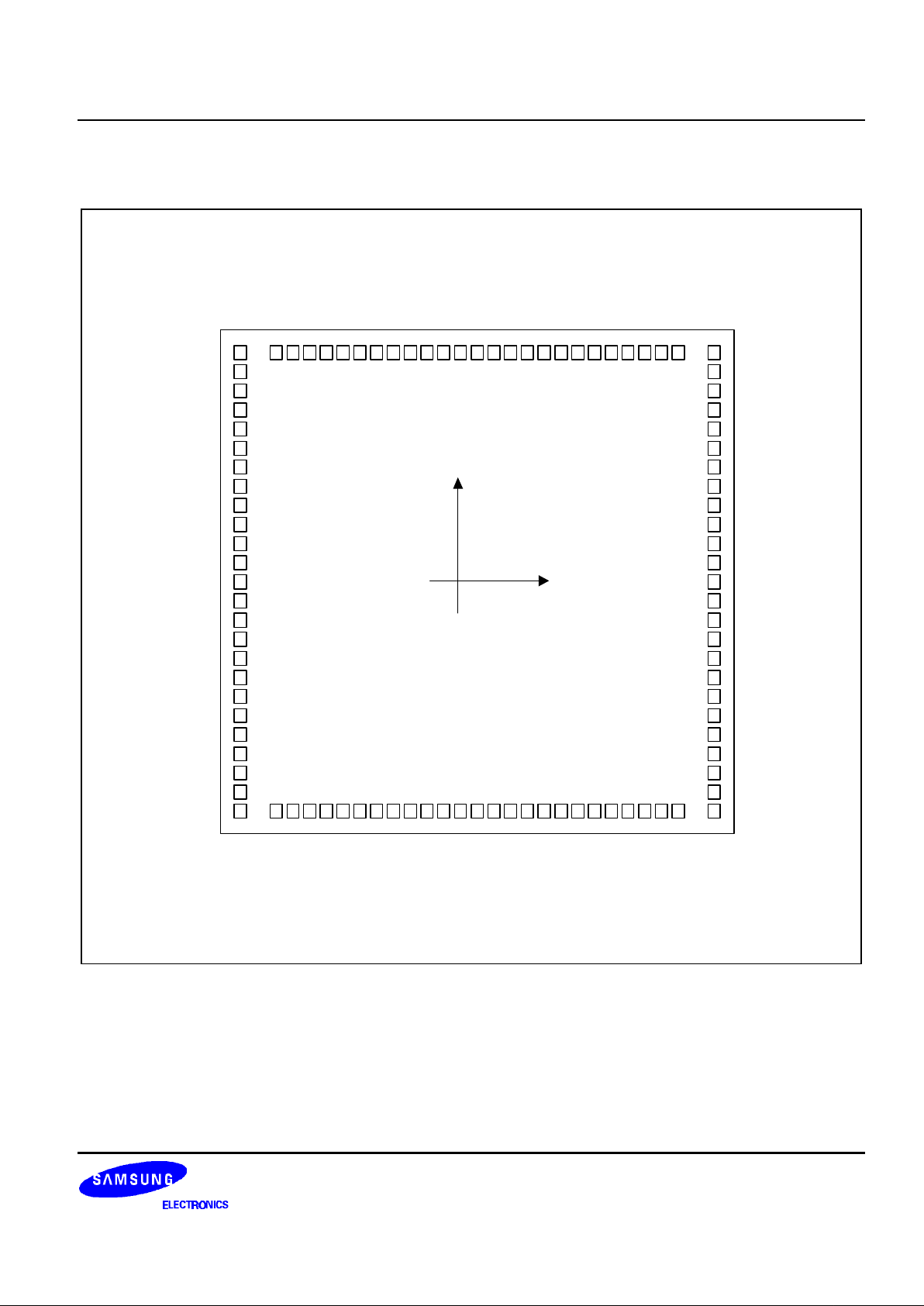
S6B0107 64CH COMMON DRIVER FOR DOT MATRIX LCD
4
PAD DIAGRAM (CHIP LAYOUT FOR THE 100QFP)
28293031323334353637383940414243444546474849505152
53
1
1009998979695949392919089888786858483828180
C22
C23
C24
C25
C26
C27
C28
C29
C30
C31
C32
C33
C34
C35
C36
C37
C38
C39
C40
C41
C42
C43
VDD
DIO1
FS
DS1
DS2
CNCR
NCCRNC
SHL
VSS
NC
MS
CLK2
CLK1
NC
FRM
M
NC
PCLK2
DIO2
NC
CL2
NC
2
3
4
5
6
7
8
9
10
11
12
13
14
15
16
17
18
19
20
21
22
23
24
25
26
27
C21
C20
C19
C18
C17
C16
C15
C14
C13
C12
C11
C10
C9
C8
C7
C6
C5
C4
C3
C2
C1
V
EE
V1L
V4L
V5L
V0L
Chip size: 3450
×
4000
PAD size: 100
×
100
Unit : µm
(0, 0) X
Y
79
78
77
76
75
74
73
72
71
70
69
68
67
66
65
64
63
62
61
60
59
58
57
56
55
54
C44
C45
C46
C47
C48
C49
C50
C51
C52
C53
C54
C55
C56
C57
C58
C59
C60
C61
C62
C63
C64
V
EE
V1R
V4R
V5R
V0R
There is the mark S6B0107 on the center of the chip.

64CH COMMON DRIVER FOR DOT MATRIX LCD S6B0107
5
PAD CENTER COORDINATES (100QFP)
Pad
Number
Pad
Name
Coordinate Pad
Number
Pad
Name
Coordinate Pad
Number
Pad
Name
Coordinate
X Y X Y X Y
1 C22 -1314.5 1775.4
32 DS2 -677.6 -1775
71 C52 1500.9 630
2 C21 -1499.9 1630 34 C -527.6 -1775
72 C51 1500.9 755
3 C20 -1499.9 1505 35 R -377.6 -1775
73 C50 1500.9 880
4 C19 -1499.9 1380 37 CR -227.6 -1775
74 C49 1500.9 1005
5 C18 -1499.9 1255 39 SHL -77.6 -1775
75 C48 1500.9 1130
6 C17 -1499.9 1130 40 VSS 113.8 -1775
76 C47 1500.9 1255
7 C16 -1499.9 1005 42 MS 308.7 -1775
77 C46 1500.9 1380
8 C15 -1499.9 880 43 CLK2 458.7 -1775
78 C45 1500.9 1505
9 C14 -1499.9 755 44 CLK1 608.7 -1775
79 C44 1500.9 1630
10 C13 -1499.9 630 46 FRM 758.7 -1775
80 C43 1310.5 1775.4
11 C12 -1499.9 505 47 M 908.7 -1775
81 C42 1185.5 1775.4
12 C11 -1499.9 380 49 PCLK2 1058.7 -1775
82 C41 1060.5 1775.4
13 C10 -1499.9 255 50 DI02 1208.7 -1775
83 C40 935.5 1775.4
14 C9 -1499.9 130 52 CL2 1358.7 -1775
84 C39 810.5 1775.4
15 C8 -1499.9
5 54 V0R 1500.9 -1495
85 C38 685.5 1775.4
16 C7 -1499.9 -120 55 V5R 1500.9 -1370
86 C37 560.5 1775.4
17 C6 -1499.9 -245 56 V4R 1500.9 -1245
87 C36 435.5 1775.4
18 C5 -1499.9 -370 57 V1R 1500.9 -1120
88 C35 310.5 1775.4
19 C4 -1499.9 -495 58 VEE 1500.9 -995 89 C34 185.5 1775.4
20 C3 -1499.9 -620 59 C64 1500.9 -870 90 C33 60.5 1775.4
21 C2 -1499.9 -745 60 C63 1500.9 -745 91 C32 -64.5 1775.4
22 C1 -1499.9 -870 61 C62 1500.9 -620 92 C31 -189.5 1775.4
23 VEE -1499.9 -995 62 C61 1500.9 -495 93 C30 -314.5 1775.4
24 V1L -1499.9 -1120
63 C60 1500.9 -370 94 C29 -439.5 1775.4
25 V4L -1499.9 -1245
64 C59 1500.9 -245 95 C28 -564.5 1775.4
26 V5L -1499.9 -1370
65 C58 1500.9 -120 96 C27 -689.5 1775.4
27 V0L -1499.9 -1495
66 C57 1500.9
5 97 C26 -814.5 1775.4
28 VDD -1345.6 -1775
67 C56 1500.9 130 98 C25 -939.5 1775.4
29 DI01 -1127.6 -1775
68 C55 1500.9 255 99 C24 -1064.5 1775.4
30 FS -977.6 -1775
69 C54 1500.9 380 100 C23 -1189.5 1775.4
31 DS1 -827.6 -1775
70 C53 1500.9 505

S6B0107 64CH COMMON DRIVER FOR DOT MATRIX LCD
6
100 TQFP (S6B2107)
C19
C18
C17
C16
C15
C14
C13
C12
C11
C10
C9C8C7C6C5C4C3C2C1
VEE
V1L
V4L
V5L
V0L
VDD
S6B2107
(100 TQFP)
12345678910111213141516171819202122232425
75747372717069686766656463626160595857565554535251
50
49
48
47
46
45
44
43
42
41
40
39
38
37
36
35
34
33
32
31
30
29
28
27
26
76
77
78
79
80
81
82
83
84
85
86
87
88
89
90
91
92
93
94
95
96
97
98
99
100
C44
C43
C42
C41
C40
C39
C38
C37
C36
C35
C34
C33
C32
C31
C30
C29
C28
C27
C26
C25
C24
C23
C22
C21
C20
NC
CL2
NC
DIO2
PCLK2
NC
M
FRM
NC
CLK1
CLK2
MS
NC
VSS
SHL
NC
CR
NC
R
NC
C
DS2
DS1
FS
DIO1
C45
C46
C47
C48
C49
C50
C51
C52
C53
C54
C55
C56
C57
C58
C59
C60
C61
C62
C63
C64
VEE
V1R
V4R
V5R
V0R
64CH COMMON DRIVER FOR DOT MATRIX LCD S6B0107
7
PAD DIAGRAM (CHIP LAYOUT FOR THE 100-TQFP)
75
74
73
72
71
70
69
68
67
66
65
64
63
62
61
60
59
58
57
56
55
54
53
52
51
26272829303132333435363738394041424344454647484950
100999897969594939291908988878685848382818079787776
C20
C21
C22
C23
C24
C25
C26
C27
C28
C29
C30
C31
C32
C33
C34
C35
C36
C37
C38
C39
C40
C41
C42
C43
C44
DIO1
FS
DS1
DS2
CNCR
NCCRNC
SHL
V
SS
NC
MS
CLK2
CLK1
NC
FRM
M
NC
PCLK2
DIO2
NC
CL2
NC
C45
C46
C47
C48
C49
C50
C51
C52
C53
C54
C55
C56
C57
C58
C59
C60
C61
C62
C63
C64
V
EE
V1R
V4R
V5R
V0R
1
2
3
4
5
6
7
8
9
10
11
12
13
14
15
16
17
18
19
20
21
22
23
24
25
C19
C18
C17
C16
C15
C14
C13
C12
C11
C10
C9
C8
C7
C6
C5
C4
C3
C2
C1
V
EE
V1L
V4L
V5L
V0L
V
DD
Chip size: 3850 X 100
PAD size: 100 X 100
Unit : µm
(0, 0) X
Y
There is the mark S6B2107 on the center of the chip.
 Loading...