

Samsung S6B0719 Datasheet
S6B0719
permission of LCD Driver IC Team.
160 SEG / 105 COM SEG DRIVER & CONTROLLER FOR STN LCD
Contents in this document are subject to change without notice. No part of this document may be reproduced or
transmitted in any form or by any means, electronic or mechanical, for any purpose, without the express written
Jan. 2000.
Ver. 0.4
Prepared by: Koo-Hyung, Jung
Chunggh@samsung.co.kr

160 SEG / 105 COM DRIVER & CONTROLLER FOR STN LCD PRELIMINARY SPEC. VER. 0.4 S6B0719
-
-
-
-
-
-
S6B0719 Specification Revision History
Version Content Date
0.0 - Original Feb.1999
0.1
0.2
- Append pad center coordinate (refer to table 2)
- Append display data RAM map (refer to figure 8)
- Modify display data RAM map (refer to figure 8)
Mar.1999
May.1999
- Append reference circuit examples (refer to page 22)
- Change the low power consumption V0 = 13V -> 15V (refer to page 1)
Modify page address circuit description ; DB3, DB2 and DB1 are “H”, but
DB1 is “L” -> DB3, DB2 and DB0 are “H”, but DB1 is “L” (refer to page 20)
0.3
- Modify set partial display duty ratio (refer to page 27)
Jun.1999
Add partial duty changing “waiting for discharging the LCD power levels
(refer to figure 34)
Change the condition of power consumption : (VDD = 3V, x6 boosting, V0 =
15V) → (VDD = 3V, x5 boosting, V0 = 13V) (refer to page 1)
Change the absolute maximum ratings of V0 and VOUT : 20V → 17V (refer
to page 50)
0.4
Change the operating voltage of V0 and VOUT : 17V → 15V (refer to page 1
Jan.2000
and 51)
Change the operating voltage of VDD : (2.4 to 5.5V) → (2.4 to 3.6V) (refer to
page 1 and 51)
- Modify Figure20 (refer to page 24)
2

S6B0719 PRELIMINARY SPEC. VER. 0.4 160 SEG / 105 COM DRIVER & CONTROLLER FOR STN LCD
CO
NTENTS
INTRODUCTION ..................................................................................................................................................1
BLOCK DIAGRAM...............................................................................................................................................2
PAD CONFIGURATION .......................................................................................................................................3
PAD CENTER COORDINATES ............................................................................................................................4
PIN DESCRIPTION ..............................................................................................................................................6
FUNCTIONAL DESCRIPTION............................................................................................................................ 11
MICROPROCESSOR INTERFACE.............................................................................................................11
DISPLAY DATA RAM (DDRAM)..................................................................................................................14
LCD DISPLAY CIRCUITS............................................................................................................................17
LCD DRIVER CIRCUIT ...............................................................................................................................19
POWER SUPPLY CIRCUITS ......................................................................................................................21
REFERENCE CIRCUIT EXAMPLES ...........................................................................................................26
RESET CIRCUIT.........................................................................................................................................28
INSTRUCTION DESCRIPTION...........................................................................................................................29
SPECIFICATIONS..............................................................................................................................................50
ABSOLUTE MAXIMUM RATINGS...............................................................................................................50
DC CHARACTERISTICS .............................................................................................................................51
AC CHARACTERISTICS............................................................................................................................. 55
REFERENCE APPLICATIONS........................................................................................................................... 59
MICROPROCESSOR INTERFACE.............................................................................................................59
CONNECTIONS BETWEEN S6B0719 AND LCD PANEL............................................................................ 60
3
S6B0719 PRELIMINARY SPEC. VER. 0.4 160 SEG / 105 COM DRIVER & CONTROLLER FOR STN LCD
INTRODUCTION
The S6B0719 is a driver & controller LSI for graphic dot-matrix liquid crystal display systems. It contains 105
common and 160 segment driver circuits. This chip is connected directly to a microprocessor, accepts serial or 8bit parallel display data and stores in an on-chip display data RAM of 105 x 160 bits. It provides a highly flexible
display section due to 1-to-1 correspondence between on-chip display data RAM bits and LCD panel pixels. And it
performs display data RAM read/write operation with no external-operating clock to minimize power consumption.
In addition, because it contains power supply circuits necessary to drive liquid crystal, it is possible to make a
display system with the fewest components.
FEATURES
Driver Output Circuits
− 105 common outputs / 160 segment outputs
Applicable Duty-ratios
Programmable duty ratio Applicable LCD bias Maximum display area
1/9 to 1/105 1/4 to 1/11
− Various partial display
− Partial window moving & data scrolling
On-chip Display Data RAM
105 × 160
− Capacity: 105 x 160 = 16,800 bits
− Bit data "1": a dot of display is illuminated
− Bit data "0": a dot of display is not illuminated
Microprocessor Interface
− 8-bit parallel bi-directional interface with 6800-series or 8080-series
− Serial interface (only write operation) available
On-chip Low Power Analog Circuit
− On-chip oscillator circuit
− Voltage converter (x3, x4, x5 or x6)
− Voltage regulator (temperature coefficient: -0.05%/°C or external input)
− On-chip electronic contrast control function (64 steps)
− Voltage follower (LCD bias: 1/4 to 1/11)
Operating Voltage Range
− Supply voltage (VDD): 2.4 to 3.6 V
− LCD driving voltage (VLCD = V0 - VSS): 4.0 to 15.0 V
Low Power Consumption
− TBD µΑ Typ. (VDD = 3V, x6 boosting, V0 = 13V, Internal power supply ON and display OFF)
− TBD µΑ Max. (during power save [standby] mode )
Package Type
− Gold bumped chip or TCP
1
160 SEG / 105 COM DRIVER & CONTROLLER FOR STN LCD PRELIMINARY SPEC. VER. 0.4 S6B0719
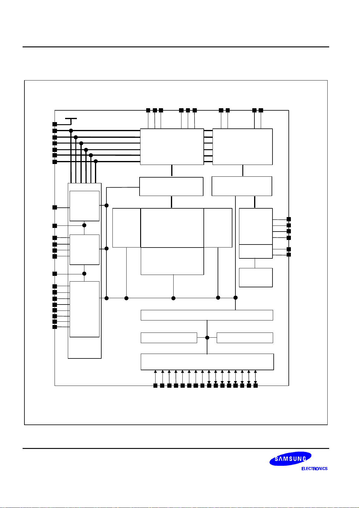
DB0
DB1
COMS
COM
3
:
:
:
7
:
:
BLOCK DIAGRAM
VDD
V0
V1
V2
V3
V4
VSS
HPMB
V0
VR
INTRS
VEXT
REF
VOUT
V/F
CIRCUIT
V/R
RCIRCUIT
PAGE
ADDRESS
CIRCUIT
SEG2
SEG1
SEG0
160 SEGMENT
DRIVER CIRCUITS
SEGMENT CONTROLLER
DISPLAY DATA RAM
105 X 160 = 16,800 Bits
COLUMN ADDRESS
CIRCUIT
SEG159SEG158SEG15
COMS
COM0
106 COMMON
DRIVER CIRCUITS
COMMON CONTROLLER
DISPLAY
LINE
ADDRESS
CIRCUIT
TIMING
GENERATOR
CIRCUIT
STATIC
DRIVER
OSCILLATOR
10
MS
CL
SYNC
M
FRS
FR
C1-
C1+
C2C2+
C3+
C4+
C5+
VCI
V/C
CIRCUIT
INSTRUCTION DECODER & REGISTER
MPU INTERFACE (PARALLEL & SERIAL)
RW_WR
E_RD
RS
CS2
CS1B
PS
C68
RESETB
Figure 1. Block Diagram
STATUS REGISTERBUS HOLDER
DB5
DB6(SCLK)
DB7(SID)
DB4
DB3
DB2
2

S6B0719 PRELIMINARY SPEC. VER. 0.4 160 SEG / 105 COM DRIVER & CONTROLLER FOR STN LCD
167
330
166
331
137
360
136
1
ðððð
- - - -
ðððð
ðððð
- - - -
ðððð
*2
*1
*3
PAD CONFIGURATION
рр ррррррррррррррррррр
- - - - - - - - - -
Y
S6B0719
(TOP VIEW)
(0,0) X
ррррррррррррррррррр
ðð
рррррррррррррррррррррр
- - - - - - - - - -
ррррррррррррррррррррррр
Figure 2. S6B0719 Chip Configuration
Table 1. S6B0719 Pad Dimensions
Size
Item Pad No.
X Y
Chip size - 9370 2220
29 to 108 70 (Min.)
Pad pitch
1 to 28, 109 to 136,
137 to 360
54 (Min.)
30 to 107 60 78
138 to 165, 332 to 359 78 44
Bumped
`pad size
3 to 27, 110 to 134
169 to 328
1, 2, 28, 29, 108, 109,
135, 136, 167, 168, 329
44 78
70 78
and 330
137, 166, 331 and 360 78 70
Bumped pad
height
30 um 30 um 30 um
1 to 360 14 (Typ.)
42 um 108 um
Unit
µm
42 um108 um
30 um 30 um 30 um
(-4033.05,-374.4)
*1 : COG Align Key *3 : ILB Align Key 2
(-3131.6,622.75)
*2 : ILB Align Key 1
42 um 108 um
42 um 108 um
(4135.6,-633.0)
3
160 SEG / 105 COM DRIVER & CONTROLLER FOR STN LCD PRELIMINARY SPEC. VER. 0.4 S6B0719
PAD CENTER COORDINATES
Table 2. Pad Center Coordinates
[Unit: µm]
NO NAME X Y NO NAME X Y NO NAME X Y NO NAME X Y
1 DUMMY -4453 -985 51 RW_WR -1225 -985 101 VR 2275 -985 151 COM13 4560 -27
2 DUMMY -4373 -985 52 E_RD -1155 -985 102 VSS 2345 -985 152 COM12 4560 27
3 COM80 -4293 -985 53 VDD -1085 -985 103 REF 2415 -985 153 COM11 4560 81
4 COM81 -4239 -985 54 DB0 -1015 -985 104 VEXT 2485 -985 154 COM10 4560 135
5 COM82 -4185 -985 55 DB1 -945 -985 105 VDD 2555 -985 155 COM9 4560 189
6 COM83 -4131 -985 56 DB2 -875 -985 106 INTRS 2625 -985 156 COM8 4560 243
7 COM84 -4077 -985 57 DB3 -805 -985 107 VSS 2695 -985 157 COM7 4560 297
8 COM85 -4023 -985 58 DB4 -735 -985 108 DUMMY 2775 -985 158 COM6 4560 351
9 COM86 -3969 -985 59 DB5 -665 -985 109 DUMMY 2917 -985 159 COM5 4560 405
10 COM87 -3915 -985 60 DB6 -595 -985 110 COM51 2997 -985 160 COM4 4560 459
11 COM88 -3861 -985 61 DB7 -525 -985 111 COM50 3051 -985 161 COM3 4560 513
12 COM89 -3807 -985 62 VDD -455 -985 112 COM49 3105 -985 162 COM2 4560 567
13 COM90 -3753 -985 63 VDD -385 -985 113 COM48 3159 -985 163 COM1 4560 621
14 COM91 -3699 -985 64 VDD -315 -985 114 COM47 3213 -985 164 COM0 4560 675
15 COM92 -3645 -985 65 VDD -245 -985 115 COM46 3267 -985 165 COMS 4560 729
16 COM93 -3591 -985 66 VCI -175 -985 116 COM45 3321 -985 166 DUMMY 4560 809
17 COM94 -3537 -985 67 VCI -105 -985 117 COM44 3375 -985 167 DUMMY 4453 985
18 COM95 -3483 -985 68 VSS -35 -985 118 COM43 3429 -985 168 DUMMY 4373 985
19 COM96 -3429 -985 69 VSS 35 -985 119 COM42 3483 -985 169 SEG0 4293 985
20 COM97 -3375 -985 70 VSS 105 -985 120 COM41 3537 -985 170 SEG1 4239 985
21 COM98 -3321 -985 71 VSS 175 -985 121 COM40 3591 -985 171 SEG2 4185 985
22 COM99 -3267 -985 72 VOUT 245 -985 122 COM39 3645 -985 172 SEG3 4131 985
23 COM100 -3213 -985 73 VOUT 315 -985 123 COM38 3699 -985 173 SEG4 4077 985
24 COM101 -3159 -985 74 C5+ 385 -985 124 COM37 3753 -985 174 SEG5 4023 985
25 COM102 -3105 -985 75 C5+ 455 -985 125 COM36 3807 -985 175 SEG6 3969 985
26 COM103 -3051 -985 76 C3+ 525 -985 126 COM35 3861 -985 176 SEG7 3915 985
27 COMS -2997 -985 77 C3+ 595 -985 127 COM34 3915 -985 177 SEG8 3861 985
28 DUMMY -2917 -985 78 C1- 665 -985 128 COM33 3969 -985 178 SEG9 3807 985
29 DUMMY -2775 -985 79 C1- 735 -985 129 COM32 4023 -985 179 SEG10 3753 985
30 FRS -2695 -985 80 C1+ 805 -985 130 COM31 4077 -985 180 SEG11 3699 985
31 FR -2625 -985 81 C1+ 875 -985 131 COM30 4131 -985 181 SEG12 3645 985
32 TEST1 -2555 -985 82 C2+ 945 -985 132 COM29 4185 -985 182 SEG13 3591 985
33 TEST2 -2485 -985 83 C2+ 1015 -985 133 COM28 4239 -985 183 SEG14 3537 985
34 TEST3 -2415 -985 84 C2- 1085 -985 134 COM27 4293 -985 184 SEG15 3483 985
35 CL -2345 -985 85 C2- 1155 -985 135 DUMMY 4373 -985 185 SEG16 3429 985
36 M -2275 -985 86 C4+ 1225 -985 136 DUMMY 4453 -985 186 SEG17 3375 985
37 SYNC -2205 -985 87 C4+ 1295 -985 137 DUMMY 4560 -809 187 SEG18 3321 985
38 VSS -2135 -985 88 VSS 1365 -985 138 COM26 4560 -729 188 SEG19 3267 985
39 HPMB -2065 -985 89 VSS 1435 -985 139 COM25 4560 -675 189 SEG20 3213 985
40 MS -1995 -985 90 V4 1505 -985 140 COM24 4560 -621 190 SEG21 3159 985
41 VDD -1925 -985 91 V4 1575 -985 141 COM23 4560 -567 191 SEG22 3105 985
42 PS -1855 -985 92 V3 1645 -985 142 COM22 4560 -513 192 SEG23 3051 985
43 C68 -1785 -985 93 V3 1715 -985 143 COM21 4560 -459 193 SEG24 2997 985
44 VSS -1715 -985 94 V2 1785 -985 144 COM20 4560 -405 194 SEG25 2943 985
45 CS1B -1645 -985 95 V2 1855 -985 145 COM19 4560 -351 195 SEG26 2889 985
46 CS2 -1575 -985 96 V1 1925 -985 146 COM18 4560 -297 196 SEG27 2835 985
47 VDD -1505 -985 97 V1 1995 -985 147 COM17 4560 -243 197 SEG28 2781 985
48 RESETB -1435 -985 98 V0 2065 -985 148 COM16 4560 -189 198 SEG29 2727 985
49
RS
50
VSS
-1365 -985 99 V0 2135 -985 149 COM15 4560 -135 199 SEG30 2673 985
-1295 -985 100 VR 2205 -985 150 COM14 4560 -81 200 SEG31 2619 985
4

S6B0719 PRELIMINARY SPEC. VER. 0.4 160 SEG / 105 COM DRIVER & CONTROLLER FOR STN LCD
Table 2 (Continued)
[Unit: µm]
NO NAME X Y NO NAME X Y NO NAME X Y NO NAME X Y
201 SEG32 2565 985 251 SEG82 -135 985 301 SEG132 -2835 985 351 COM71 -4560 -297
202 SEG33 2511 985 252 SEG83 -189 985 302 SEG133 -2889 985 352 COM72 -4560 -351
203 SEG34 2457 985 253 SEG84 -243 985 303 SEG134 -2943 985 353 COM73 -4560 -405
204 SEG35 2403 985 254 SEG85 -297 985 304 SEG135 -2997 985 354 COM74 -4560 -459
205 SEG36 2349 985 255 SEG86 -351 985 305 SEG136 -3051 985 355 COM75 -4560 -513
206 SEG37 2295 985 256 SEG87 -405 985 306 SEG137 -3105 985 356 COM76 -4560 -567
207 SEG38 2241 985 257 SEG88 -459 985 307 SEG138 -3159 985 357 COM77 -4560 -621
208 SEG39 2187 985 258 SEG89 -513 985 308 SEG139 -3213 985 358 COM78 -4560 -675
209 SEG40 2133 985 259 SEG90 -567 985 309 SEG140 -3267 985 359 COM79 -4560 -729
210 SEG41 2079 985 260 SEG91 -621 985 310 SEG141 -3321 985 360 DUMMY -4560 -809
211 SEG42 2025 985 261 SEG92 -675 985 311 SEG142 -3375 985
212 SEG43 1971 985 262 SEG93 -729 985 312 SEG143 -3429 985
213 SEG44 1917 985 263 SEG94 -783 985 313 SEG144 -3483 985
214 SEG45 1863 985 264 SEG95 -837 985 314 SEG145 -3537 985
215 SEG46 1809 985 265 SEG96 -891 985 315 SEG146 -3591 985
216 SEG47 1755 985 266 SEG97 -945 985 316 SEG147 -3645 985
217 SEG48 1701 985 267 SEG98 -999 985 317 SEG148 -3699 985
218 SEG49 1647 985 268 SEG99 -1053 985 318 SEG149 -3753 985
219 SEG50 1593 985 269 SEG100 -1107 985 319 SEG150 -3807 985
220 SEG51 1539 985 270 SEG101 -1161 985 320 SEG151 -3861 985
221 SEG52 1485 985 271 SEG102 -1215 985 321 SEG152 -3915 985
222 SEG53 1431 985 272 SEG103 -1269 985 322 SEG153 -3969 985
223 SEG54 1377 985 273 SEG104 -1323 985 323 SEG154 -4023 985
224 SEG55 1323 985 274 SEG105 -1377 985 324 SEG155 -4077 985
225 SEG56 1269 985 275 SEG106 -1431 985 325 SEG156 -4131 985
226 SEG57 1215 985 276 SEG107 -1485 985 326 SEG157 -4185 985
227 SEG58 1161 985 277 SEG108 -1539 985 327 SEG158 -4239 985
228 SEG59 1107 985 278 SEG109 -1593 985 328 SEG159 -4293 985
229 SEG60 1053 985 279 SEG110 -1647 985 329 DUMMY -4373 985
230 SEG61 999 985 280 SEG111 -1701 985 330 DUMMY -4453 985
231 SEG62 945 985 281 SEG112 -1755 985 331 DUMMY -4560 809
232 SEG63 891 985 282 SEG113 -1809 985 332 COM52 -4560 729
233 SEG64 837 985 283 SEG114 -1863 985 333 COM53 -4560 675
234 SEG65 783 985 284 SEG115 -1917 985 334 COM54 -4560 621
235 SEG66 729 985 285 SEG116 -1971 985 335 COM55 -4560 567
236 SEG67 675 985 286 SEG117 -2025 985 336 COM56 -4560 513
237 SEG68 621 985 287 SEG118 -2079 985 337 COM57 -4560 459
238 SEG69 567 985 288 SEG119 -2133 985 338 COM58 -4560 405
239 SEG70 513 985 289 SEG120 -2187 985 339 COM59 -4560 351
240 SEG71 459 985 290 SEG121 -2241 985 340 COM60 -4560 297
241 SEG72 405 985 291 SEG122 -2295 985 341 COM61 -4560 243
242 SEG73 351 985 292 SEG123 -2349 985 342 COM62 -4560 189
243 SEG74 297 985 293 SEG124 -2403 985 343 COM63 -4560 135
244 SEG75 243 985 294 SEG125 -2457 985 344 COM64 -4560 81
245 SEG76 189 985 295 SEG126 -2511 985 345 COM65 -4560 27
246 SEG77 135 985 296 SEG127 -2565 985 346 COM66 -4560 -27
247 SEG78 81 985 297 SEG128 -2619 985 347 COM67 -4560 -81
248 SEG79 27 985 298 SEG129 -2673 985 348 COM68 -4560 -135
249 SEG80 -27 985 299 SEG130 -2727 985 349 COM69 -4560 -189
250 SEG81 -81 985 300 SEG131 -2781 985 350 COM70 -4560 -243
5

160 SEG / 105 COM DRIVER & CONTROLLER FOR STN LCD PRELIMINARY SPEC. VER. 0.4 S6B0719
PIN DESCRIPTION
Table 3. Power Supply Pins
Name I/O Description
VDD Supply Power supply
Vss Supply Ground
LCD drivers supply voltages
The voltage determined by LCD pixel is impedance-converted by an operational amplifier
V0
V1
V2
V3
V4
I/O
for application.
Voltages should have the following relationship: V0 ≥ V1 ≥ V2 ≥ V3 ≥ V4 ≥ Vss
When the internal power circuit is active, these voltages are generated as following table
according to the state of LCD bias.
LCD bias V1 V2 V3 V4
1/N bias (N-1)/N x V0 (N-2)/N x V0 2/N x V0 1/N x V0
NOTE : *N = 4 to 11
Table 4. LCD Driver Supply Pins
Name I/O Description
C1-, C2- I/O Capacitor negative connection pins for voltage converter
C1+, C2+
C3+, C4+
C5+
VOUT I/O Voltage converter input/output pin
VCI I
VR I
REF I
VEXT I
I/O Capacitor positive connection pins for voltage converter
Voltage converter input voltage pin
Voltages should have the following relationship: VDD ≤ VCI ≤ V0
V0 voltage adjustment pin
It is valid only when on-chip resistors are not used. (INTRS = “L”)
Selects the external VREF voltage via VEXT pin
− REF = "L": using the external VREF
− REF = "H": using the internal VREF
Externally input reference voltage (VREF) for the internal voltage regulator.
It is valid only when REF is “L”.
6

S6B0719 PRELIMINARY SPEC. VER. 0.4 160 SEG / 105 COM DRIVER & CONTROLLER FOR STN LCD
Table 5. System Control Pins
Name I/O Description
Master / Slave operations select pin
− MS = "H": master operation
− MS = "L": slave operation
The following table depends on the MS status.
MS I
CL I/O
SYNC I/O
M I/O
FR O
FRS O
INTRS I
HPMB I
TEST1
to
TEST3
MS
Internal analog circuits Display timing signals
Oscillator Power supply CL SYNC M
H Enabled Enabled Output Output Output
L Disabled Disabled Input Input Input
Display clock input / output pin
When the S6B0719 is used in master / slave mode (multi-chip), the CL pins must be
connected each other.
Display sync input / output pin
When the S6B0719 is used in master/slave mode (multi-chip), the SYNC pins must be
connected each other.
LCD AC input / output pin
When the S6B0719 is used in master/slave mode (multi-chip), the M pins must be
connected each other.
Static driver common output pin
This pin is used together with the FRS pin.
Static driver segment output pin
This pin is used together with the FR pin.
Internal resistors select pin
This pin selects the resistors for adjusting V0 voltage level.
− INTRS = "H”: use the internal resistors.
− INTRS = "L”: use the external resistors. VR pin and external resistive divider control V0
voltage.
Power control pin of the power supplies circuit for LCD driver
− HPMB = "L": high power mode
− HPMB = "H": normal mode
This pin is valid in master operation.
Test pins
I
Don’ t use these pins.
NOTE: DUMMY – These pins should be opened (floated).
7

160 SEG / 105 COM DRIVER & CONTROLLER FOR STN LCD PRELIMINARY SPEC. VER. 0.4 S6B0719
Table 6. Microprocessor Interface Pins
Name I/O Description
RESETB I
PS I
C68 I
CS1B
CS2
RS I
RW_WR I
Reset input pin
When RESETB is “L”, initialization is executed.
Parallel / Serial data input select input
PS Interface
mode
H Parallel RS DB0 to DB7
Data /
instruction
Data Read / Write Serial clock
E_RD
RW_WR
L Serial RS SID (DB7) Write only SCLK (DB6)
*NOTE: When PS is “L”, DB0 to DB5 are high impedance and E_RD and RW_WR
must be fixed to either “H” or “L”.
Microprocessor interface select input pin
− C68 = "H": 6800-series MPU interface
− C68 = "L": 8080-series MPU interface
Chip select input pins
Data / instruction I/O is enabled only when CS1B is “L” and CS2 is “H”.
I
When chip select is non-active, DB0 to DB7 may be high impedance.
Register select input pin
− RS = "H": DB0 to DB7 are display data
− RS = "L": DB0 to DB7 are control data
Read / Write execution control pin
C68 MPU Type RW_WR Description
Read/Write control input pin
H 6800-series RW
− RW = “H”: read
− RW = “L”: write
Write enable clock input pin
L 8080-series /WR
The data on DB0 to DB7 are latched at the rising
edge of the /WR signal.
-
8
S6B0719 PRELIMINARY SPEC. VER. 0.4 160 SEG / 105 COM DRIVER & CONTROLLER FOR STN LCD
Table 6. (Continued)
Name I/O Description
Read / Write execution control pin
C68 MPU Type E_RD Description
Read / Write control input pin
− RW = “H”: When E is “H”, DB0 to DB7 are in an
output status.
− RW = “L”: The data on DB0 to DB7 are latched at
E_RD I
H 6800-series E
the falling edge of the E
signal.
L 8080-series /RD
Read enable clock input pin
When /RD is “L”, DB0 to DB7 are in an output status.
8-bit bi-directional data bus that is connected to the standard 8-bit microprocessor data
DB0
to
DB7
I/O
bus. When the serial interface selected (PS = "L");
− DB0 to DB5: high impedance
− DB6: serial input clock (SCLK)
− DB7: serial input data (SID).
When chip select is not active, DB0 to DB7 may be high impedance.
9
160 SEG / 105 COM DRIVER & CONTROLLER FOR STN LCD PRELIMINARY SPEC. VER. 0.4 S6B0719
Table 7. LCD driver output pins
Name I/O Description
LCD segment driver outputs
The display data and the M signal control the output voltage of segment driver.
SEG0
to
SEG159
COM0
to
COM103
COMS O
Display data M
Segment driver output voltage
Normal display Reverse display
H H V0 V2
O
H L Vss V3
L H V2 V0
L L V3 Vss
Power save mode Vss Vss
LCD common driver outputs
The internal scanning data and M signal control the output voltage of common driver.
Scan data M Common driver output voltage
H H Vss
O
H L V0
L H V1
L L V4
Power save mode Vss
Common output for the icons
The output signals of two pins are same. When not used, these pins should be left open.
10

S6B0719 PRELIMINARY SPEC. VER. 0.4 160 SEG / 105 COM DRIVER & CONTROLLER FOR STN LCD
FUNCTIONAL DESCRIPTION
MICROPROCESSOR INTERFACE
Chip Select Input
There are CS1B and CS2 pins for chip selection. The S6B0719 can interface with an MPU only when CS1B is “L”
and CS2 is “H”. When these pins are set to any other combination, RS, E_RD, and RW_WR inputs are disabled
and DB0 to DB7 are to be high impedance. And, in case of serial interface, the internal shift register and the
counter are reset.
Parallel / Serial Interface
The S6B0719 has three types of interface with an MPU, which are one serial and two parallel interfaces. This
parallel or serial interface is determined by PS pin as shown in table 8.
Table 8. Parallel / Serial Interface Mode.
PS Type CS1B CS2 C68 Interface mode
H Parallel CS1B CS2
L Serial CS1B CS2
Parallel Interface (PS = "H")
The 8-bit bi-directional data bus is used in parallel interface and the type of MPU is selected by C68 as shown in
table 9. The type of data transfer is determined by signals at RS, E_RD and RW_WR as shown in table 10.
Table 9. Microprocessor Selection for Parallel Interface
C68 CS1B CS2 RS E_RD RW_WR DB0 to DB7 MPU bus
H CS1B CS2 RS E RW DB0 to DB7 6800-series
L CS1B CS2 RS /RD /WR DB0 to DB7 8080-series
Table 10. Parallel Data Transfer
Common 6800-series 8080-series Description
RS
E_RD
(E)
RW_WR
(RW)
E_RD
(/RD)
RW_WR
(/WR)
H 6800-series MPU mode
L 8080-series MPU mode
*×
Serial-mode
*×: Don't care
H H H L H Display data read out
H H L H L Display data write
L H H L H Register status read
L H L H L Writes to internal register (instruction)
11

160 SEG / 105 COM DRIVER & CONTROLLER FOR STN LCD PRELIMINARY SPEC. VER. 0.4 S6B0719
Serial Interface (PS = "L")
When the S6B0719 is active, serial data (DB7) and serial clock (DB6) inputs are enabled. And not active, the
internal 8-bit shift register and the 3-bit counter are reset. Serial data can be read on the rising edge of serial clock
going into DB6 and processed as 8-bit parallel data on the eighth serial clock. Serial data input is display data when
RS is high and control data when RS is low. Since the clock signal (DB6) is easy to be affected by the external
noise caused by the line length, the operation check on the actual machine is recommended.
CS1B
CS2
SID
SCLK
RS
DB6DB7DB0DB1DB2DB3DB4DB5DB6DB7
Figure 3. Serial Interface Timing
Busy Flag
The Busy Flag indicates whether the S6B0719 is operating or not. When DB7 is “H” in read status operation, this
device is in busy status and will accept only read status instruction. If the cycle time is correct, the microprocessor
needs not to check this flag before each instruction, which improves the MPU performance.
12

S6B0719 PRELIMINARY SPEC. VER. 0.4 160 SEG / 105 COM DRIVER & CONTROLLER FOR STN LCD
RS
DB0 to DB7
BUS HOLDER
N
D(N)
D(N+1)
D(N+2)
N
N+1
N+2
N+3
Data Transfer
The S6B0719 uses bus holder and internal data bus for data transfer with the MPU. When writing data from the
MPU to on-chip RAM, data is automatically transferred from the bus holder to the RAM as shown in figure 4. And
when reading data from on-chip RAM to the MPU, the data for the initial read cycle is stored in the bus holder
(dummy read) and the MPU reads this stored data from bus holder for the next data read cycle as shown in figure 5.
This means that a dummy read cycle must be inserted between each pair of address sets when a sequence of
address sets is executed. Therefore, the data of the specified address cannot be output with the read display data
instruction right after the address sets, but can be output at the second read of data.
MPU signals
RS
/WR
DB0 to DB7
Internal signals
/WR
BUS HOLDER
COLUMN ADDRESS
MPU signals
/WR
/RD
Internal signals
/WR
N D(N) D(N+1) D(N+2) D(N+3)
N D(N) D(N+1) D(N+2) D(N+3)
N N+1 N+2 N+3
Figure 4. Write Timing
N
Dummy D(N) D(N+1)
/RD
COLUMN ADDRESS
Figure 5. Read Timing
13

160 SEG / 105 COM DRIVER & CONTROLLER FOR STN LCD PRELIMINARY SPEC. VER. 0.4 S6B0719
- -
- -
- -
- -
001
- -
0
011
- -
0
101
- -
0
000
- -
1
DISPLAY DATA RAM (DDRAM)
The Display Data RAM stores pixel data for the LCD. It is 105-row by 160-column addressable array. Each pixel
can be selected when the page and column addresses are specified. The 105 rows are divided into 13 pages of 8
lines and the 13th page with a single line (DB0 only). Data is read from or written to the 8 lines of each page directly
through DB0 to DB7. The display data of DB0 to DB7 from the microprocessor correspond to the LCD common
lines as shown in figure 6. The microprocessor can read from and write to RAM through the I/O buffer. Since the
LCD controller operates independently, data can be written into RAM at the same time as data is being displayed
without causing the LCD flicker.
DB0
DB1
DB2
DB3
DB4
1 0 0 - - 1
COM0
COM1
COM2
COM3
COM4
- -
Display Data RAM LCD Display
Figure 6. RAM-to-LCD Data Transfer
Page Address Circuit
This circuit is for providing a Page Address to Display Data RAM shown in figure 8. It incorporates 4-bit Page
Address register changed by only the “Set Page” instruction. Page Address 13 (DB3, DB2 and DB0 are “H”, but
DB1 is “L”) is a special RAM area for the icons and display data DB0 is only valid.
Line Address Circuit
This circuit assigns DDRAM a line address corresponding to the first line (COM0) of the display. Therefore, by
setting line address repeatedly, it is possible to realize the screen scrolling and page switching without changing
the contents of on-chip RAM as shown in figure 7. It incorporates 7-bit line address register changed by only the
initial display line instruction and 7-bit counter circuit. At the beginning of each LCD frame, the contents of register
are copied to the line counter which is increased by CL signal and generates the Line Address for transferring the
160-bit RAM data to the display data latch circuit. However, display data of icons are not scrolled because the MPU
can not access Line Address of icons.
14

S6B0719 PRELIMINARY SPEC. VER. 0.4 160 SEG / 105 COM DRIVER & CONTROLLER FOR STN LCD
Column Address Circuit
Column Address circuit has an 8-bit preset counter that provides Column Address to the Display Data RAM as
shown in figure 8. When set Column Address MSB / LSB instruction is issued, 8-bit [Y7:Y0] is updated. And, since
this address is increased by 1 each a read or write data instruction, microprocessor can access the display data
continuously. However, the counter is not incremented and locked if a non-existing address above 9FH. It is
unlocked if a column address is set again by set Column Address MSB / LSB instruction. And the Column Address
counter is independent of page address register.
ADC select instruction makes it possible to invert the relationship between the Column Address and the segment
outputs. It is necessary to rewrite the display data on built-in RAM after issuing ADC select instruction. Refer to the
following figure 7.
SEG Output
SEG
0
SEG
1
SEG
2
SEG
3
... ...
SEG
156
SEG
157
SEG
158
SEG
159
Column address [Y7:Y0] 00H 01H 02H 03H ... ... 9CH 9DH 9EH 9FH
Display data 1 0 1 0 1 1 0 0
LCD panel display
... ...
( ADC = 0 )
LCD panel display
( ADC = 1 )
... ...
Figure 7. The Relationship between the Column Address and The Segment Outputs
Segment Control Circuit
This circuit controls the display data by the display ON / OFF, reverse display ON / OFF and entire display ON /
OFF instructions without changing the data in the display data RAM.
15

160 SEG / 105 COM DRIVER & CONTROLLER FOR STN LCD PRELIMINARY SPEC. VER. 0.4 S6B0719
Page Address
DB3 DB0DB1DB2
0 000
0 100
0 010
0 110
1 100
1 010
1 110
1 001
1 101 DB0 -
Column Address
LCD Segment Output
Data
DB0
DB1
DB2
DB3
DB4
DB5
DB6
DB7
DB0
DB1
DB2
DB3
DB4
DB5
DB6
DB7
DB0
DB1
DB2
DB3
DB4
DB5
DB6
DB7
DB0
DB1
DB2
DB3
DB4
DB5
DB6
DB7
DB0
DB1
DB2
DB3
DB4
DB5
DB6
DB7
DB0
DB1
DB2
DB3
DB4
DB5
DB6
DB7
DB0
DB1
DB2
DB3
DB4
DB5
DB6
DB7
DB0
DB1
DB2
DB3
DB4
DB5
DB6
DB7
ADC=0
ADC=1
00
SEG0
02
SEG1
SEG2
0301 04 05
9C9D 9A9B9E9F
SEG3
SEG4
SEG5
Page 0
Page 1
Page 2
Page 3
Page 9
Page 10
Page 11
Page 12
Page 13
- - - - - - - -
- - - - - - - -
- - - - - - - -
9C9D9A9B 9E 9F
SEG154
SEG155
0203 00010405
SEG156
SEG157
SEG158
SEG159
Line
Address
00H
01H
02H
03H
04H
05H
06H
07H
08H
09H
0AH
0BH
0CH
0DH
0EH
0FH
10H
11H
12H
13H
14H
15H
16H
17H
18H
19H
1AH
1BH
1CH
1DH
1EH
1FH
48H
49H
4AH
4BH
4CH
4DH
4EH
4FH
50H
51H
52H
53H
54H
55H
56H
57H
58H
59H
5AH
5BH
5CH
5DH
5EH
5FH
60H
61H
62H
63H
64H
65H
66H
67H
End = 07H
Start = 08H
1/97 Duty
1/105 Duty
Initial start line
address = 08H
COM
Output
COM0
COM1
COM2
COM3
COM4
COM5
COM6
COM7
COM8
COM9
COM10
COM11
COM12
COM13
COM14
COM15
COM16
COM17
COM18
COM19
COM20
COM21
COM22
COM23
COM24
COM25
COM26
COM27
COM28
COM29
COM30
COM31
COM72
COM73
COM74
COM75
COM76
COM77
COM78
COM79
COM80
COM81
COM82
COM83
COM84
COM85
COM86
COM87
COM88
COM89
COM90
COM91
COM92
COM93
COM94
COM95
COM96
COM97
COM98
COM99
COM100
COM101
COM102
COM103
COMS
16
Figure 8. Display Data RAM Map

S6B0719 PRELIMINARY SPEC. VER. 0.4 160 SEG / 105 COM DRIVER & CONTROLLER FOR STN LCD
LCD DISPLAY CIRCUITS
Oscillator
This is completely on-chip Oscillator and its frequency is nearly independent of VDD. This oscillator signal is used in
the voltage converter and display timing generation circuit.
Display Timing Generator Circuit
This circuit generates some signals to be used for displaying LCD. The display clock, CL, generated by oscillation
clock, generates the clock for the line counter and the signal for the display data latch. The line address of on-chip
RAM is generated in synchronization with the display clock (CL) and the display data latch circuit in synchronization
latches the 160-bit display data with the display clock. The display data, which is read to the LCD driver, is
completely independent of the access to the display data RAM from the microprocessor. The display clock
generates an LCD AC signal (M) which enables the LCD driver to make a AC drive waveform, and also generates
an internal common timing signal and start signal to the common driver. The frame or the line changes the phase of
M by setting internal instruction. Driving waveform and internal timing signal are shown in figure 10.
In a multiple-chip configuration, the slave chip requires the CL, M and SYNC signals from the master. Table 11
shows the CL, SYNC, and M status.
Table 11. Master and Slave Timing Signal Status
Operation mode Oscillator CL SYNC M
Master ON (internal clock used) Output Output Output
Slave OFF (external clock used) Input Input Input
17
 Loading...