

Samsung S6B0708 Datasheet

64COM/128SEG GRAPHIC DRIVER FOR DOT MATRIX LCD
S6B0708
INTRODUCTION
S6B0708 is a single-chip LCD driver IC for liquid crystal dot-matrix graphic display systems. It incorporates 192
driver circuit for 64 common and 128 segment and 64 x 128-bit bit-map RAM. It is capable of interfacing with the
microprocessor, accepting 8-bit parallel display data directly from it, and storing data in an one chip display data
RAM. And it generates internal signals for using LCD driving independent of microprocessor clock.
FEATURES
• 64-channel common & 128-channel segment driver for dot matrix LCD
• On-chip display data RAM: 64 × 128 = 8192bits
• Display data is stored in display data RAM from MPU
- RAM bit data: ON(1), OFF(0)
• Internal timing generator circuit for dynamic display
• 8-bit parallel bi-directional data bus
• Applicable LCD duty: 1/64
• Power supply voltages: Power supply voltage range: 4.5 - 5.5V (VDD)
• LCD driving voltage range: 8.0 - 17.0V (VLCD = VDD-VEE)
• Wide operating temperature range: Ta = -30°C - 85°C
• High voltage CMOS process
• Gold bumped chip available
1

S6B0708 64COM/128SEG GRAPHIC DRIVER FOR DOT MATRIX
C1 ... C32 S1 S2 ... S63 S64 S65 S66 ... S127 S128 C33...C64
RE
LCD
BLOCK DIAGRAM
VDD
V0
V1
V2
V3
V4
V5
VEE
VSS
FS
CR
...
32
Channel
Common
32bit Shift
Reg
64-Bit Data Latch 64-Bit Data Latch
Display
Timing
Generator
Circuit
Page & Line
Decoder
C
R
Oscillator
64 X 64 = 4,096 Bits
... ... ...
64 Channel
Segment
Driver
Display Data RAM
Column Decoder Column Decoder
64 Channel
Segment
Driver
Display Data RAM
64 X 64 = 4,096 Bits
32
Channel
Common
32bit Shift
Reg
Page & Line
Decoder
SHL
PCLK2
ADC
RAM Address Register RAM Address Register
Status
Register
Instruction
Decoder
DB0 - DB7
CS1B
Instruction
Decoder
I/O Register I/O BufferI/O Buffer
4
Status
Register
E
SETB
RS
RW
CS2B
2

64COM/128SEG GRAPHIC DRIVER FOR DOT MATRIX LCD
S6B0708
PAD CONFIGURATION
219
250
218
1
S6B0708
Y
(0, 0) X
86
85
54
53
Item Pad No. Size Unit
X Y
Chip size - 12590 3630
Pad pitch - 90 (min.)
Bumped pad size 1 - 53 56 140
54 - 85 140 56
86 - 218 56 140
219 - 250 140 56
Bumped pad height All Pad 17 (typ.)
µm
3
S6B0708 64COM/128SEG GRAPHIC DRIVER FOR DOT MATRIX
LCD
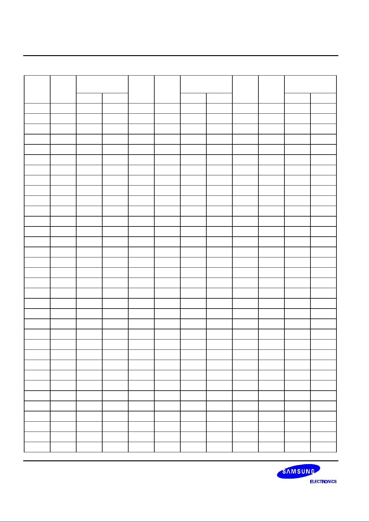
PAD CENTER COORDINATES
Pad No. Pad
Name
X Y X Y X Y
1 Dummy -6115 -1600 35 CS2B 1343 -1600 69 C16 6115 -36.5
2 Dummy -6025 -1600 36 C 1563 -1600 70 C17 6115 53.5
3 Dummy -5935 -1600 37 CR 1783 -1600 71 C18 6115 143.5
4 VEE -5477 -1600 38 R 2003 -1600 72 C19 6115 233.5
5 VEE -5257 -1600 39 DB0 2175 -1600 73 C20 6115 323.5
6 VEE -5037 -1600 40 DB1 2467 -1600 74 C21 6115 413.5
7 V5 -4817 -1600 41 DB2 2759 -1600 75 C22 6115 503.5
8 V5 -4597 -1600 42 DB3 3051 -1600 76 C23 6115 593.5
9 V5 -4377 -1600 43 DB4 3343 -1600 77 C24 6115 683.5
10 V4 -4157 -1600 44 DB5 3635 -1600 78 C25 6115 773.5
11 V4 -3937 -1600 45 DB6 3927 -1600 79 C26 6115 863.5
12 V4 -3717 -1600 46 DB7 4219 -1600 80 C27 6115 953.5
13 V3 -3497 -1600 47 RS 4559 -1600 81 C28 6115 1043.5
14 V3 -3277 -1600 48 RW 4779 -1600 82 C29 6115 1133.5
15 V3 -3057 -1600 49 E 4999 -1600 83 C30 6115 1223.5
16 V2 -2837 -1600 50 CS1B 5219 -1600 84 C31 6115 1313.5
17 V2 -2617 -1600 51 RESETB 5439 -1600 85 C32 6115 1403.5
18 V2 -2397 -1600 52 Dummy 6025 -1600 86 Dummy
19 V1 -2177 -1600 53 Dummy 6115 -1600 87 Dummy
20 V1 -1957 -1600 54 C1 6115 -1386.5
21 V1 -1737 -1600 55 C2 6115 -1296.5
22 V0 -1517 -1600 56 C3 6115 -1206.5
23 V0 -1297 -1600 57 C4 6115 -1116.5
24 V0 -1077 -1600 58 C5 6115 -1026.5
25 VDD -857 -1600 59 C6 6115 -936.5 93 S6 5265 1635
26 VDD -637 -1600 60 C7 6115 -846.5 94 S7 5175 1635
27 VDD -417 -1600 61 C8 6115 -756.5 95 S8 5085 1635
28 VSS -197 -1600 62 C9 6115 -666.5 96 S9 4995 1635
29 VSS 23 -1600 63 C10 6115 -576.5 97 S10 4905 1635
30 VSS 243 -1600 64 C11 6115 -486.5 98 S11 4815 1635
31 PCLK2
32 FS 683 -1600 66 C13 6115 -306.5 100 S13 4635 1635
33 SHL 903 -1600 67 C14 6115 -216.5
34 ADC 1123 -1600 68 C15 6115 -126.5
Coordinate Pad No. Pad
Name
463 -1600 65 C12 6115 -396.5 99 S12 4725 1635
Coordinate Pad No. Pad
Name
88 S1 5715 1635
89 S2 5625 1635
90 S3 5535 1635
91 S4 5445 1635
92 S5 5355 1635
Coordinate
6115 1635
6025 1635
4
64COM/128SEG GRAPHIC DRIVER FOR DOT MATRIX LCD
S6B0708
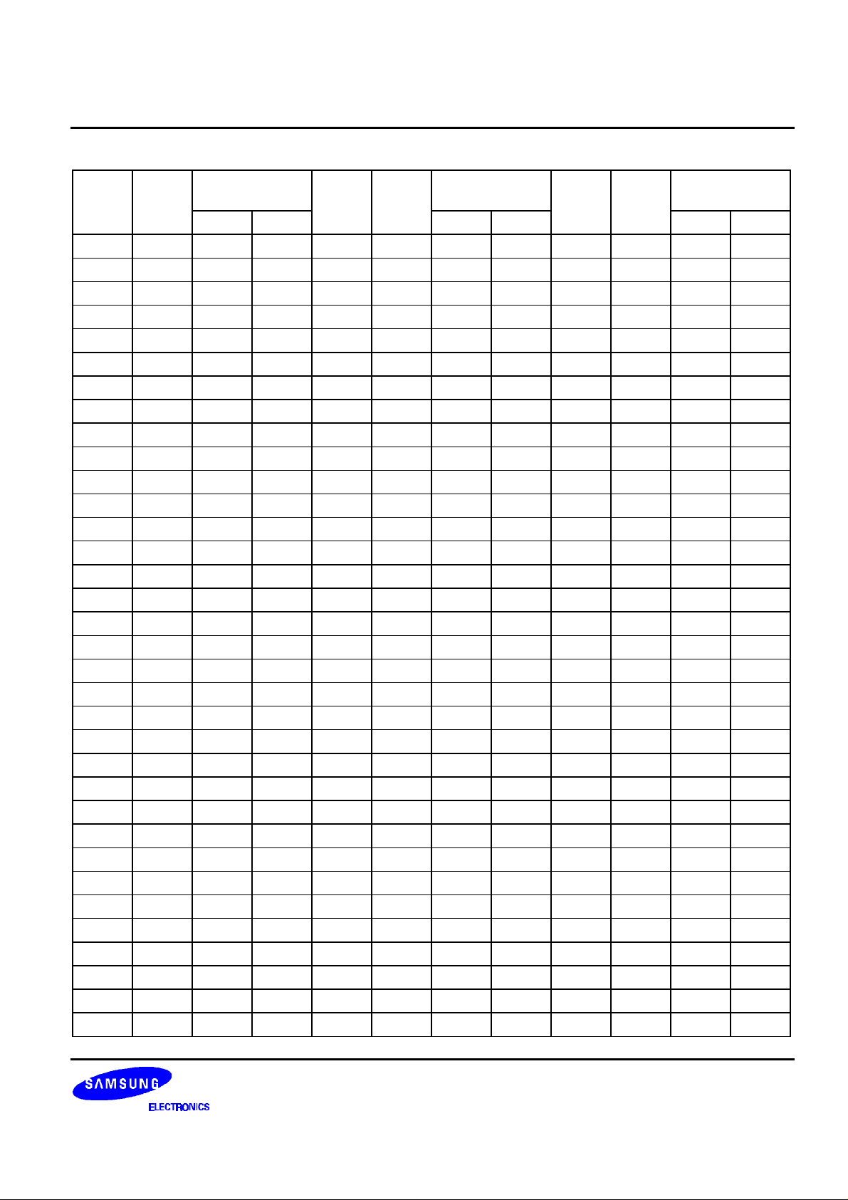
Table 1. Pad Center Coordinates (Continued)
Pad
No.
X Y X Y X Y
101 S14 4545 1635 135 S48 1485 1635 169 S82 -1575 1635
102 S15 4455 1635 136 S49 1395 1635 170 S83 -1665 1635
103 S16 4365 1635 137 S50 1305 1635 171 S84 -1755 1635
104 S17 4275 1635 138 S51 1215 1635 172 S85 -1845 1635
105 S18 4185 1635 139 S52 1125 1635 173 S86 -1935 1635
106 S19 4095 1635 140 S53 1035 1635 174 S87 -2025 1635
107 S20 4005 1635 141 S54 945 1635 175 S88 -2115 1635
108 S21 3915 1635 142 S55 855 1635 176 S89 -2205 1635
109 S22 3825 1635 143 S56 765 1635 177 S90 -2295 1635
110 S23 3735 1635 144 S57 675 1635 178 S91 -2385 1635
111 S24 3645 1635 145 S58 585 1635 179 S92 -2475 1635
112 S25 3555 1635 146 S59 495 1635 180 S93 -2565 1635
113 S26 3465 1635 147 S60 405 1635 181 S94 -2655 1635
114 S27 3375 1635 148 S61 315 1635 182 S95 -2745 1635
115 S28 3285 1635 149 S62 225 1635 183 S96 -2835 1635
116 S29 3195 1635 150 S63 135 1635 184 S97 -2925 1635
117 S30 3105 1635 151 S64 45 1635 185 S98 -3015 1635
118 S31 3015 1635 152 S65 -45 1635 186 S99 -3105 1635
119 S32 2925 1635 153 S66 -135 1635 187 S100 -3195 1635
120 S33 2835 1635 154 S67 -225 1635 188 S101 -3285 1635
121 S34 2745 1635 155 S68 -315 1635 189 S102 -3375 1635
122 S35 2655 1635 156 S69 -405 1635 190 S103 -3465 1635
123 S36 2565 1635 157 S70 -495 1635 191 S104 -3555 1635
124 S37 2475 1635 158 S71 -585 1635 192 S105 -3645 1635
125 S38 2385 1635 159 S72 -675 1635 193 S106 -3735 1635
126 S39 2295 1635 160 S73 -765 1635 194 S107 -3825 1635
127 S40 2205 1635 161 S74 -855 1635 195 S108 -3915 1635
128 S41 2115 1635 162 S75 -945 1635 196 S109 -4005 1635
129 S42 2025 1635 163 S76 -1035 1635 197 S110 -4095 1635
130 S43 1935 1635 164 S77 -1125 1635 198 S111 -4185 1635
131 S44 1845 1635 165 S78 -1215 1635 199 S112 -4275 1635
132 S45 1755 1635 166 S79 -1305 1635 200 S113 -4365 1635
133 S46 1665 1635 167 S80 -1395 1635
134 S47 1575 1635 168 S81 -1485 1635
Pad
Name
Coordinate Pad
No.
Pad
Name
Coordinate Pad
No.
Pad
Name
Coordinate
5

S6B0708 64COM/128SEG GRAPHIC DRIVER FOR DOT MATRIX
LCD
Table 1. Pad Center Coordinates (Continued)
Pad
No.
X Y X Y X Y
201 S114 -4455 1635 235 C48 -6115 -36.5
202 S115 -4545 1635 236 C47 -6115 -126.5
203 S116 -4635 1635 237 C46 -6115 -216.5
204 S117 -4725 1635 238 C45 -6115 -306.5
205 S118 -4815 1635 239 C44 -6115 -396.5
206 S119 -4905 1635 240 C43 -6115 -486.5
207 S120 -4995 1635 241 C42 -6115 -576.5
208 S121 -5085 1635 242 C41 -6115 -666.5
209 S122 -5175 1635 243 C40 -6115 -756.5
210 S123 -5265 1635 244 C39 -6115 -846.5
211 S124 -5355 1635 245 C38 -6115 -936.5
212 S125 -5445 1635 246 C37 -6115 -1026.5
213 S126 -5535 1635 247 C36 -6115 -1116.5
214 S127 -5625 1635 248 C35 -6115 -1206.5
215 S128 -5715 1635 249 C34 -6115 -1296.5
216 Dummy -5935 1635 250 C33 -6115 -1386.5
217 Dummy -6025 1635
218 Dummy -6115 1635
219 C64 -6115 1403.5
220 C63 -6115 1313.5
221 C62 -6115 1223.5
222 C61 -6115 1133.5
223 C60 -6115 1043.5
224 C59 -6115 953.5
225 C58 -6115 863.5
226 C57 -6115 773.5
227 C56 -6115 683.5
228 C55 -6115 593.5
229 C54 -6115 503.5
230 C53 -6115 413.5
231 C52 -6115 323.5
232 C51 -6115 233.5
233 C50 -6115 143.5
234 C49 -6115 53.5
Pad
Name
Coordinate Pad
No.
Pad
Name
Coordinate Pad
No.
Pad
Name
Coordinate
6

64COM/128SEG GRAPHIC DRIVER FOR DOT MATRIX LCD
S6B0708
CRCRCfRf
S6B0708
PAD DESCRIPTION
POWER SUPPLY
Name I/O Type Description
VDD Supply Power supply. connect to MPU power supply pin VCC
VSS Supply Ground
VEE Supply For LCD driver circuit
V0, V1
V2, V3
V4, V5
OSCILLATOR
Supply
LCD driver supply voltages
The voltages must satisfy the following relationship
VDD ≥ V0 ≥ V1 ≥ V2 ≥ V3 ≥ V4 ≥ V5 ≥ VEE
Name I/O Type
C
O
RC oscillator
- Internal clock
CR
R
I
O
- External clock
FS I Frequency selection
When the frame frequency is 70Hz, the oscillation frequency should be as the
following table.
FS
H
L
Open
Oscillation Frequency
Fosc = 430kHz
Fosc = 215kHz
Description
S6B0708
CR CR
External
clock
Open
7

S6B0708 64COM/128SEG GRAPHIC DRIVER FOR DOT MATRIX
Display data DB[7:0] can be written at falling edge of E.
LCD
MICROPROCESSOR INTERFACE
Name I/O Type
CS1B I First chip(S1 ~ S64) select input.
Data input/output is enabled via E, RS, RW, and DB[0:7]when CS1B = Low.
CS2B I Second chip(S65 ~ S128) select input.
Data input/output is enabled via E, RS, RW, and DB[0:7] when CS2B = Low.
RS I Register selection
RS
H
L
The data in DB[7:0] is display data.
The data in DB[7:0] is control data.
Description
RW I Read or write
RW
H
L
Data appears at DB[7:0] when E = high.
Description
E Enable signal.
DB0 - DB7
E
H
L
Read data in DB[7:0] appears while E = high.
Display data DB[7:0] is latched at falling edge of E.
I/O Data bus [0 - 7]
Description
Bi-directional data bus
Description
8

64COM/128SEG GRAPHIC DRIVER FOR DOT MATRIX LCD
S6B0708
RESET
Name I/O Type
Description
RESETB I Reset input
Chip is initialized when RESETB is low
LCD DRIVER OUTPUTS
Name I/O Type
Description
C1 - C64 O LCD driver common output
S1 - S128
O LCD driver segment output
PCLK2 I Phase of internal shift clock (CLK2)
PCLK2
H
L
Data shift at the rising edge of CLK2
Data shift at the falling edge of CLK2
Phase of Internal Shift Clock (CLK2)
ADC I Address control signal of Y address counter.
ADC
H
S1 → S2 ..... S63 → S65 → S66 ..... S127 → S128
L
S64 → S63 ..... S2 → S1 → S128 → S127..... S66 → S65
Segment Output Direction
SHL I Selection of data shift direction
SHL
H
C1 → C2 → C3 ..... C62 → C63 → C64
L
C64 → C63 → C62 ..... C3 → C2 → C1
Data Shift Direction
9
 Loading...