

Samsung S6B0086 Datasheet

80 CH SEGMENT / COMMON DRIVER FOR DOT MATRIX LCD
S6B0086
June. 2000.
Ver. 0.0
Contents in this document are subject to change without notice. No part of this document may be reproduced
or transmitted in any form or by any means, electronic or mechanical, for any purpose, without the express
written permission of LCD Driver IC Team.
S6B0086 80CH COMMON / SEGMENT DRIVER FOR DOT MATRIX LCD
INTRODUCTION
The S6B0086 is an LCD driver LSI which is fabricated by low power CMOS high voltage process technology. In
segment driver mode, it can be interfaced in 1-bit serial or 4-bit parallel method by the controller. In common
driver mode, dual type mode is applicable. And in segment mode application, the power down function reduces
power consumption.
FEATURES
• Power supply voltage: + 5V ± 10 %, + 3V ± 10%
• Supply voltage for display: 6 to 28V (VDD-VEE)
• 4-bit parallel / 1-bit serial data processing (in segment mode)
• Single mode operation / dual mode operation (in common mode)
• Power down function (in segment mode)
• Applicable LCD duty: 1/64 – 1/256
• Interface
DRIVERS
COM (cascade) SEG (cascade)
S6B0086 S6B0086
• High voltage CMOS process
• Bare die or TCP available
2

80CH COMMON / SEGMENT DRIVER FOR DOT MATRIX LCD S6B0086
TCP
S
S
S
S
S
S
NCNCN
S
C
C
C
C
C
C
C
C
8
7
7
7
7
7
0
9
8
7
6
5
----------------SC
7
4
S
S
S
S
S
S
C
C
C
C
C
7
6
5
4
3
2
C
1
NCNCN
C
S6B0086
D
I
M
S
V
P
0
F
F
B
S
D
H
D
L
E
V
R
E
B
E
#1 #20
V
V
5
V
4
3
V0C
1
2
S
D
D
V
4
3
S
-
-
S
D
D
R
M
D
D
1
2
D
L
C
A
C
-
L
S
I
M
2
S
E
L
L
1
B
D
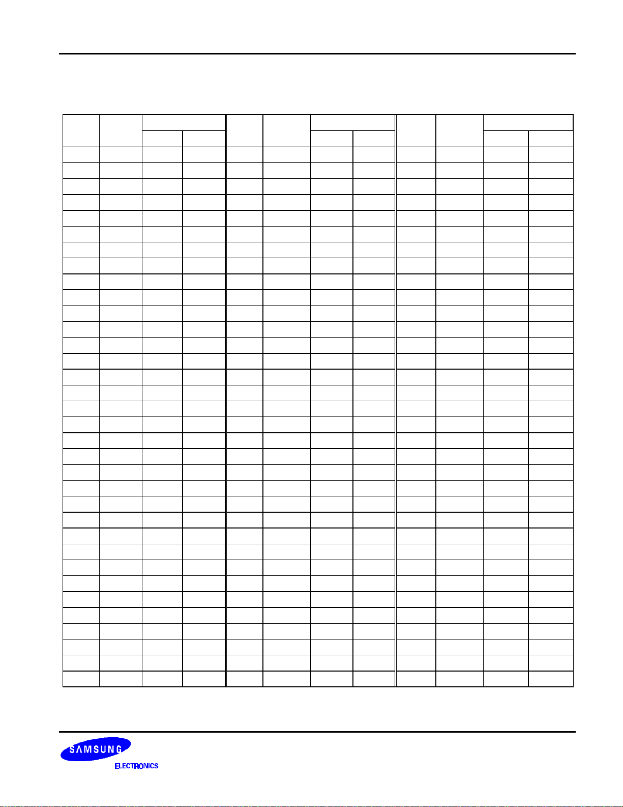
* Package Type = 100-TCP-35mm
* Input Lead Pitch = 0.80mm
* Output Lead Pitch = 0.22mm
3

S6B0086 80CH COMMON / SEGMENT DRIVER FOR DOT MATRIX LCD
DISPOFFB
PAD DIAGRAM (S6B0086 / S6B0086 TCP)
SC51
SC50
SC49
SC48
SC47
SC46
SC45
SC44
SC43
SC42
SC41
SC40
SC39
SC38
SC37
SC36
SC35
SC34
SC33
SC32
SC31
SC30
1
1009998979695949392919089888786858483828180
79
SC52
SC53
SC54
SC55
SC56
SC57
SC58
SC59
SC60
SC61
SC62
SC63
SC64
SC65
SC66
SC67
SC68
SC69
SC70
SC71
SC72
SC73
SC74
SC75
SC76
SC77
SC78
SC79
SC80
10
11
12
13
14
15
16
17
18
19
20
21
22
23
24
25
26
27
28
29
30
2
3
4
5
6
7
8
9
Y
98
×
X
4390
S6B0086
(0, 0)
Chip size: 4530
Pad size: 98
Unit: µm
×
78
77
76
75
74
73
72
71
70
69
68
67
66
65
64
63
62
61
60
59
58
57
56
55
54
53
52
51
SC29
SC28
SC27
SC26
SC25
SC24
SC23
SC22
SC21
SC20
SC19
SC18
SC17
SC16
SC15
SC14
SC13
SC12
SC11
SC10
SC9
SC8
SC7
SC6
SC5
SC4
SC3
SC2
SC1
31323334353637383940414243444546474849
V5
V43
ERB
VEE
V12
V0
CS
M
VDD
SHL
VSS
D4_DR
D3_DM
D2_DL
D1_SID
CL2
AMS
CL1
50
ELB
4
80CH COMMON / SEGMENT DRIVER FOR DOT MATRIX LCD S6B0086
PAD CENTER COORDINATES (S6B0086 / S6B0086TCP)
Pad
No.
Pad
Name
Coordinates Coordinates Coordinates
X Y
Pad
No.
Pad
Name
X Y
Pad
No.
Pad
Name
X Y
1 SC51 -1690 1959 35 V12 -900 -1959 69 SC19 2029 544
2 SC52 -2029 1884 36 V0 -775 -1959 70 SC20 2029 678
3 SC53 -2029 1750 37 VS -600 -1959 71 SC21 2029 812
4 SC54 -2029 1616 38 M -475 -1959 72 SC22 2029 946
5 SC55 -2029 1482 39
DISP0FFB
-350 -1959 73 SC23 2029 1080
6 SC56 -2029 1348 40 VDD -225 -1959 74 SC24 2029 1214
7 SC57 -2029 1214 41 SHL -100 -1959 75 SC25 2029 1348
8 SC58 -2029 1080 42 VSS 25 -1959 76 SC26 2029 1482
9 SC59 -2029 946 43 D4_DR 266 -1959 77 SC27 2029 1616
10 SC60 -2029 812 44 D3_DM 470 -1959 78 SC28 2029 1750
11 SC61 -2029 678 45 D2_DL 711 -1959 79 SC29 2029 1884
12 SC62 -2029 544 46 D1_SID 915 -1959 80 SC30 1690 1959
13 SC63 -2029 410 47 CL2 1040 -1959 81 SC31 1529 1959
14 SC64 -2029 276 48 ELB 1165 -1959 82 SC32 1368 1959
15 SC65 -2029 142 49 CL1 1290 -1959 83 SC33 1207 1959
16 SC66 -2029 8 50 ELB 1496 -1959 84 SC34 1046 1959
17 SC67 -2029 -126 51 SC1 2029 -1884 85 SC35 885 1959
18 SC68 -2029 -260 52 SC2 2029 -1735 86 SC36 724 1959
19 SC69 -2029 -394 53 SC3 2029 -1601 87 SC37 563 1959
20 SC70 -2029 -528 54 SC4 2029 -1467 88 SC38 402 1959
21 SC71 -2029 -662 55 SC5 2029 -1333 89 SC39 241 1959
22 SC72 -2029 -797 56 SC6 2029 -1199 90 SC40 80 1959
23 SC73 -2029 -931 57 SC7 2029 -1065 91 SC41 -80 1959
24 SC74 -2029 -1065 58 SC8 2029 -931 92 SC42 -241 1959
25 SC75 -2029 -1199 59 SC9 2029 -797 93 SC43 -402 1959
26 SC76 -2029 -1333 60 SC10 2029 -662 94 SC44 -563 1959
27 SC77 -2029 -1467 61 SC11 2029 -528 95 SC45 -724 1959
28 SC78 -2029 -1601 62 SC12 2029 -394 96 SC46 -885 1959
29 SC79 -2029 -1735 63 SC13 2029 -260 97 SC47 -1046 1959
30 SC80 -2029 -1884 64 SC14 2029 -126 98 SC48 -1207 1959
31 ERB -1479 -1959 65 SC15 2029 8 99 SC49 -1368 1959
32 VEE -1275 -1959 66 SC16 2029 142 100 SC50 -1529 1959
33 V5 -1150 -1959 67 SC17 2029 276
34 V43 -1025 -1959 68 SC18 2029 410
5
S6B0086 80CH COMMON / SEGMENT DRIVER FOR DOT MATRIX LCD
BLOCK DIAGRAM
V0
V12
V43
V5
VEE
DISP0FFB
SC1 SC2 SC3
SC78SC79SC80
80-bit 4-level Driver
80-bit Driver
M
Output
Level
D1_SID
Selector
D2_DL
LCK
80-bit Data Latch/
Common Data bi-directional shift register
D3_DM
D4_DR
CL1
CL2
CS
AMS
Clock
Control
SCK
20 x 4-bit Segment Data
bi-directional Shift Register
Data Latch Control
Power
Down
Function
ELB
ERB
VDD
VSS
6
80CH COMMON / SEGMENT DRIVER FOR DOT MATRIX LCD S6B0086
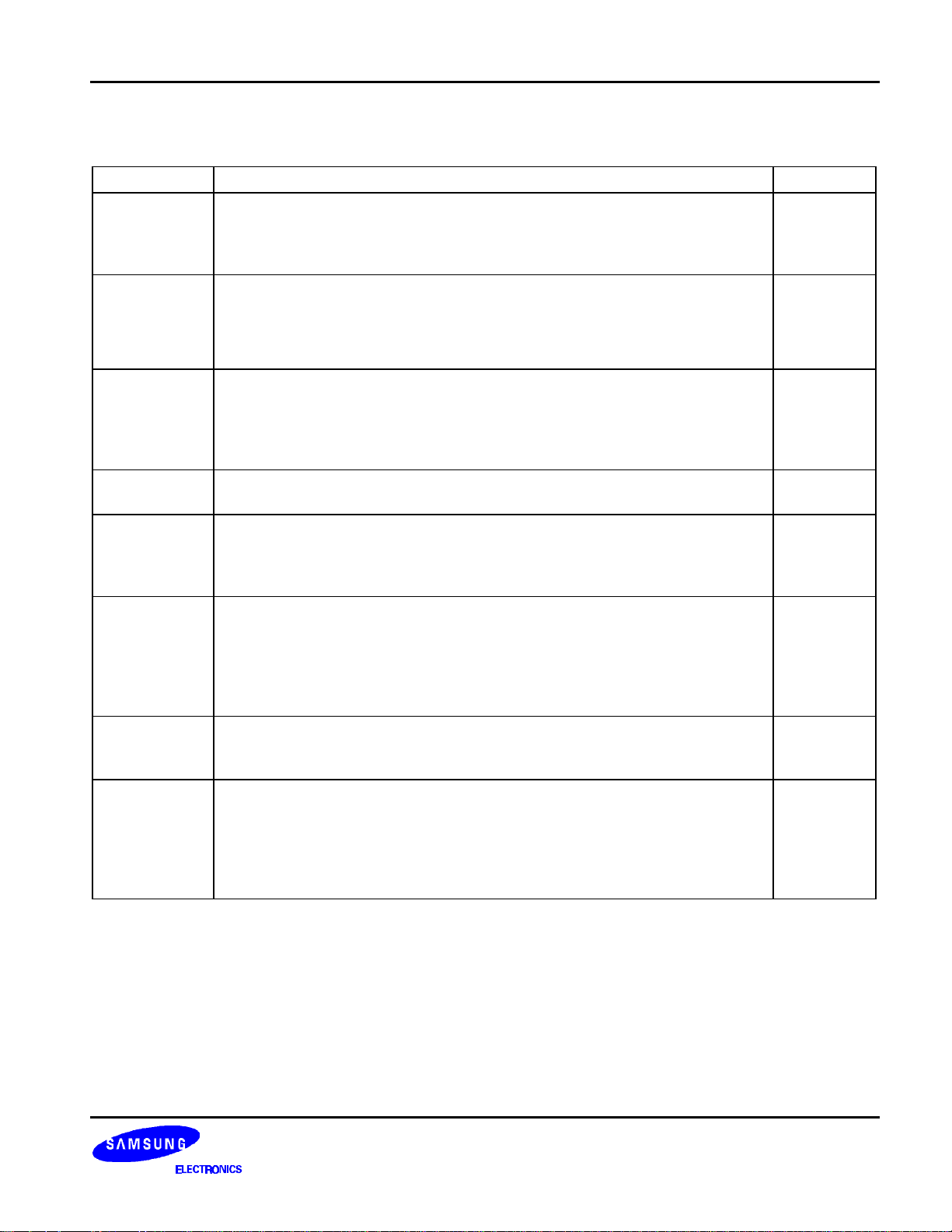
BLOCK DESCRIPTION
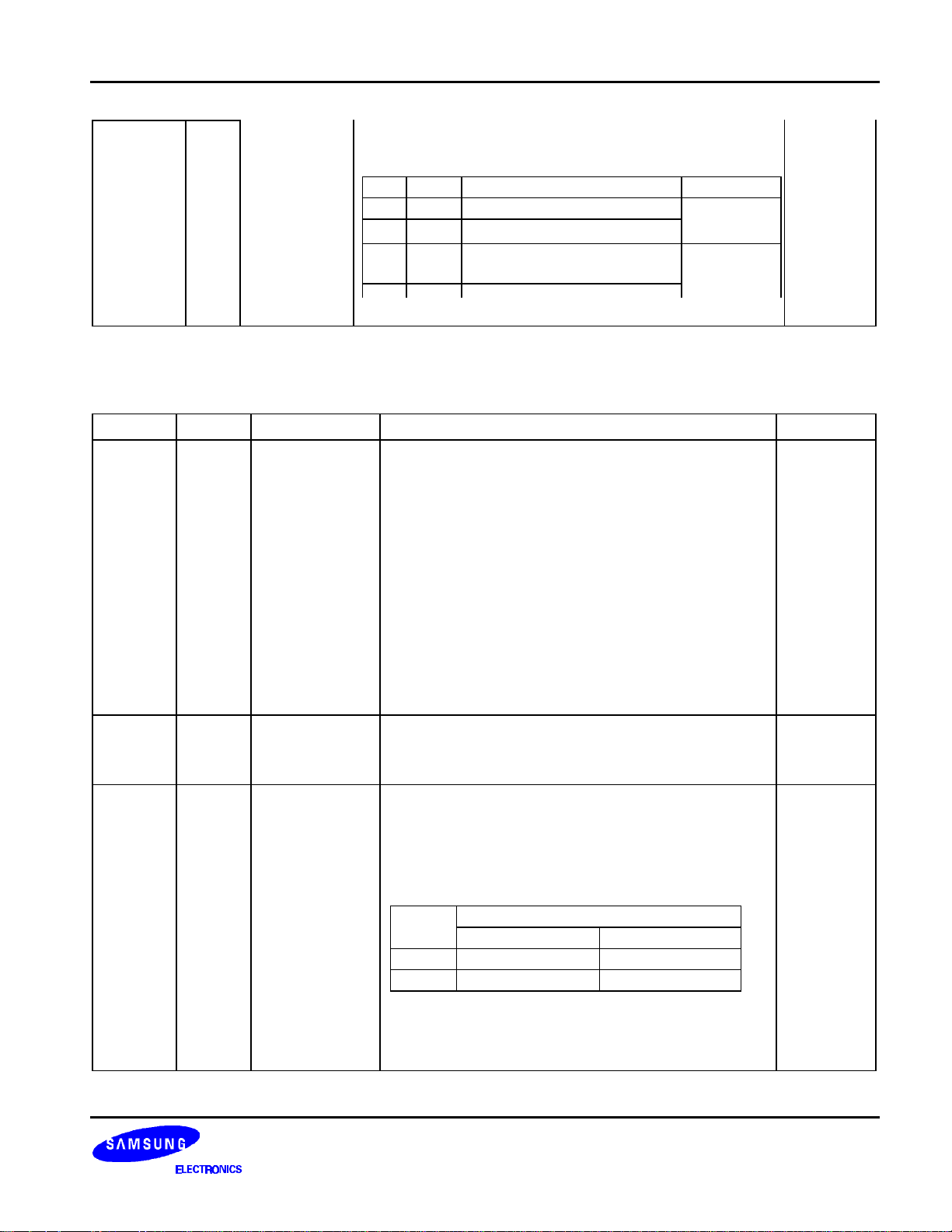
Name Function COM / SEG
Generates latch clock (LCK), shift clock (SCK) and control clock timing
Clock control
Data latch
control
Power down
function
Output level
selector
20x4-bit
segment data
I-directional
shift register
80-bit data
latch /
common data
I-directional
shift register
80-bit level
shifter
80-bit 4-level
driver
according to the input of CL1, CL2 and control inputs (CS, AMS). In common
driver application mode, this block generates the shift clock (LCK) for the
common data Bi-directional shift register.
Determines the direction of segment data shift, and input data of each
Bi-directional shift register. In 4-bit segment data parallel transfer mode, data
is shifted by a 4-bit unit. In common driver application mode, data is
transferred to the common data shift register directly, which disables this
block.
Controls the clock enable state of the current driver according to the input
value of enable pin (ELB or ERB). If enable input value is “Low”, every clock
of the current driver is enabled and the clock control block works. But if
enable input is “High”, current driver is disabled and the input data value has
no effect on the output level. So power consumption can be lowered.
Controls the output voltage level according to the input control pin (M and
DISPOFFB) (refer to PIN DESCRIPTION).
Stores output data value by shifting the input values. In 1-bit serial interface
mode application, all 80 shift clocks (SCK) are needed to store all the display
data. But in 4-bit parallel transfer mode application, only 20 clocks are
needed. In common driver application mode, this block does not work.
In segment driver application mode, the data from the 20x4-bit segment data
shift register are latched for segment driver output. In single-type common
driver application,1-bit input data (from DL or DR pin) is shifted and latched
by the direction according to the SHL signal input. In dual-type common
application mode, 80-bit registers are divided by two blocks and controlled
independently (refer to NOTE 3).
Voltage level shifter block for high voltage part. The inputs of this block are of
logical voltage level and the outputs of this block are at high voltage level
value. These values are input in to the driver.
Selects the output voltage level according to M and latched data value. If the
data value is "High" the driver output is at selected voltage level (V0 or V5),
and in the reverse case the driver output value is at the non-selected level
(V12 or V43). In segment driver application mode, non-selected output value
is V2 or V3. and when in common driver application, this value becomes V1
or V4.
COM / SEG
SEG
SEG
COM / SEG
SEG
COM / SEG
SEG
SEG
7

S6B0086 80CH COMMON / SEGMENT DRIVER FOR DOT MATRIX LCD
PIN DESCRIPTION
Pin I / O Name Function Interface
VDD Logical "High" input port (+5V ± 10%, +3V ± 10%)
VSS 0V (GND)
VEE
V0, V12,
V43, V5
SC1 - SC80 O
CL2 I
I
Power supply
LCD driver
output voltage
level
LCD driver
output
Data shift
clock
Logical "Low" for high voltage part
Bias supply voltage input to drive the LCD. Bias voltage divided
by the resistance is usually used as a supply voltage source
(refer to NOTE 2).
Display data output pin which corresponds to the respective latch
contents. One of V0, V12, V34 and V5 is selected as a display
driving voltage source according to the combination of the
latched data level and M signal (refer to NOTE 1).
Clock pulse input for the bi-directional shift register.
– In segment driver application mode, the data is shifted to 20 x
4-bit segment data shift
The clock pulse, which was input when the enable bit
(ELB/ERB) is in not active condition, is invalid.
– In common driver application mode, the data is shifted to 80-bit
common data bi-directional shift register by the CL1 clock.
Hence, this clock pin is not used (Open or connect this pin to
VDD).
Power
Power
LCD
Controller
M I
CL1 I
DISPOFFB I
CS I
AC signal for
LCD driver
output
Data latch
clock
Display OFF
control
COM / SEG
mode control
Alternate signal input pin for LCD driving.
Normal frame inversion signal is input in to this pin.
– In segment driver application mode, this signal is used for
latching the shift register contents at the falling edge of this clock
pulse.
CL1 pulse "High" level initializes power-down function block.
– In common driver application mode, CL1 is used as a shifting
clock of common output data.
Control input pin to fix the driver output (SC1~SC80) to V0 level,
during "Low" value input. LCD becomes non-selected by V0 level
output from every output of segment drivers and every output of
common drivers.
When CS = "Low", S6B0086 is used as an 80-bit segment driver.
When CS = "High", S6B0086 is set to an 80-bit common driver
Controller
Controller
Controller
VDD / VSS
8
80CH COMMON / SEGMENT DRIVER FOR DOT MATRIX LCD S6B0086
According to the input value of the AMS and the CS pin,
application mode of S6B0086 is differs as shown below.
CS AMS Application mode COM/SEG
AMS I
Application
mode select
0 0 4-bit parallel interface mode
0 1 1-bit serial interface mode
1 0
Single type application
mode
VDD / VSS
COM
PIN DESCRIPTION (CONTINUED)
Pin I / O Name Function Interface
In segment driver application mode, these pins are
used as 4-bit data input pin (when 4-bit parallel
interface mode : AMS = "Low"), or D1_SID is used as
serial data input pin and other pins are not used
(connect these to VDD) (when 1-bit serial interface
mode : AMS = "High").
– In common driver application mode, the data is
shifted from D2_DL(D4_DR) to D4_DR(D2_DL), when
in single type interface mode (AMS = "Low"). In dualtype application case, the data are shifted from
D2_DL and D3_DM (D4_DR and D3_DM) to
D4_DR(D2_DL). In each case the direction of the data
shift and the connection of data pins are determined
by SHL input (refer to NOTE 3, NOTE 4).
Controller
D1_SID,
D2_DL,
D3_DM,
D4_DR
I / O
Display data
input / serial
input data / left,
right data input
output
SHL Input
ELB,
ERB
I / O
Shift direction
control
Enable data
input/output
When SHL = "Low", data is shifted from left to right.
When SHL = "High", the direction is reversed. (refer
to NOTE3)
– In segment driver application mode, the internal
operation is enabled only when enable input (ELB
or ERB) is “Low” (power down function). When
several drivers are serially connected, the enable
state of each driver is shifted according to the
SHL input. Connect these pins as below.
Segment Driver
ELB ERB
L Output (open) Input (VSS)
H Input (VSS) Output (open)
- In common driver application mode, power down
function is not used.
Open these pins.
VDD/VSS
9

S6B0086 80CH COMMON / SEGMENT DRIVER FOR DOT MATRIX LCD
NOTE 1. Output Level Control
M Latched data DISPOFFB
Output level (SC1 – SC80)
SEG Mode COM Mode
L L H V12 (V2) V12 (V1)
L H H V0 V5
H L H V43 (V3) V43 (V4)
H H H V5 V0
X X L V0 V0
10
 Loading...