

Samsung S6A0070, S6A1070 Datasheet

80 SEG / 16 COM DRIVER & CONTROLLER FOR DOT MATRIX LCD
June. 2000.
Ver. 0.0
S6A0070
Contents in this document are subject to change without notice. No part of this document may be reproduced
or transmitted in any form or by any means, electronic or mechanical, for any purpose, without the express
written permission of LCD Driver IC Team.

S6A0070 80 SEG / 16 COM DRIVER & CONTROLLER FOR DOT MATRIX LCD
2
INTRODUCTION
The S6A0070 is a dot matrix LCD driver & controller LSI which is fabricated by low power CMOS technology.
It is capable of displaying 1 or 2 lines with the 5 × 7 format or 1 line with the 5 × 10 dots format.
The mirror type of S6A0070: S6A1070
FUNCTION
• Character type dot matrix LCD driver & controller
• Internal driver: 16 common and 80 segment signal output
• Easy Interface with a 4-bit or 8-bit MPU
• Display character pattern: 5 × 7 dots format (192 kinds), 5 × 10 dots format (32 kinds)
• The special character pattern is directly programmable by the Character Generator RAM.
• A customer character pattern is programmable by mask option.
• It can drive a maximum 80 characters by using the S6A0065 or S6A2067 externally.
• Various instruction functions
• Built-in automatic power on reset
• Driving method is A-type (line inversion)
FEATURES
• Internal Memory
- Character Generator ROM: 8320bits (192 cha. X 5 x 7 dots) & (32 cha. X 5 x 10 dots)
- Character Generator RAM: 64 x 8 bits (8 cha. X 5 x 7 dots)
- Display Data RAM: 80 × 8 bits for 80 digits (80 characters max.)
• Power Supply Voltage: 2.7 to 5.5 V (VDD)
• LCD Driving Voltage: 3.0 to 10.0 V (VDD - V5)
• Supply Voltage for display: 0 to -5V (V5)
• Programmable duty cycle: 1/8 duty, 1/11 duty or 1/16
• Internal oscillator with an external resistor
• Bare die or bumped chip available
80 SEG / 16 COM DRIVER & CONTROLLER FOR DOT MATRIX LCD S6A0070
3
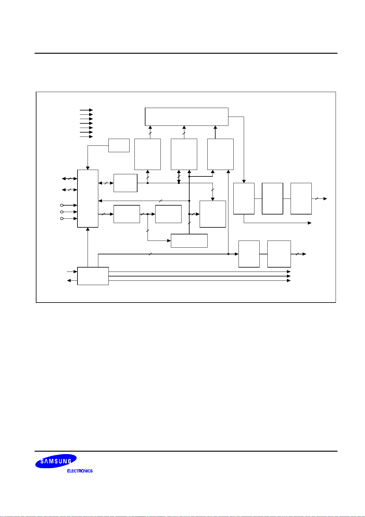
BLOCK DIAGRAM
VDD
GND
V1
V2
Parallel/Serial
Data Conversion Circuit
Busy
Flag
Character
Generator
ROM
(CGROM)
8320 bits
Character
Generator
RAM
(CGRAM)
512 bits
Cursor
& Blink
Controller
Circuit
55
Input/
Output
Buffer
Data
Register
(DR)
Instruction
Register
(IR)
Instruction
Decoder
(ID)
Address
Counter (AC)
Display
Data RAM
(DDRAM)
640 bits
Timing
Generator
Circuit
16-bit
Shift
Register
16-bit
Common
Driver
80-bit
Shift
Register
80-bit
Latch
Circuit
Segment
Driver
R/W
RS
E
DB0-DB3
DB4-DB7
OSC1
OSC2
CLK1
CLK2
M
D
SEG1SEG80
COM1COM16
8
8
8
8
7
8
7
8
8
7
7
16
80
4
4
V3
V4
V5
S6A0070 80 SEG / 16 COM DRIVER & CONTROLLER FOR DOT MATRIX LCD
4
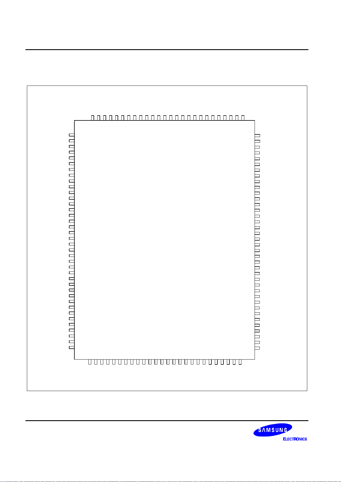
PIN CONFIGURATION
S6A0070
SEG34
SEG35
SEG36
SEG37
SEG38
SEG39
SEG40
SEG41
SEG42
SEG43
SEG44
SEG45
SEG46
SEG47
SEG48
SEG49
SEG50
SEG51
SEG52
SEG53
SEG54
SEG55
SEG56
SEG57
SEG58
SEG59
128
127
126
125
124
123
122
121
120
119
118
117
116
115
114
113
112
111
110
109
108
107
106
105
104
103
NC
SEG33
SEG32
SEG31
SEG30
SEG29
SEG28
SEG27
SEG26
SEG25
SEG24
SEG23
SEG22
SEG21
SEG20
SEG19
SEG18
SEG17
SEG16
SEG15
SEG14
SEG13
SEG12
SEG11
SEG10
SEG9
SEG8
SEG7
SEG6
SEG5
SEG4
SEG3
SEG2
SEG1
VSS
OSC2
OSC1
NC
1
2
3
4
5
6
7
8
9
10
11
12
13
14
15
16
17
18
19
20
21
22
23
24
25
26
27
28
29
30
31
32
33
34
35
36
37
38
39404142434445464748495051525354555657585960616263
64
NCNCNC
V1V2V3V4V5
CLK1
CLK2
M
D
RS
R/W
E
VDD
DB0
DB1
DB2
DB3
DB4
DB5
DB6
DB7
TEST
NC
102
101
100
99
98
97
96
95
94
93
92
91
90
89
88
87
86
85
84
83
82
81
80
79
78
77
76
75
74
73
72
71
70
69
68
67
66
65
SEG60
SEG61
SEG62
SEG63
SEG64
SEG65
SEG66
SEG67
SEG68
SEG69
SEG70
SEG71
SEG72
SEG73
SEG74
SEG75
SEG76
SEG77
SEG78
SEG79
SEG80
COM16
COM15
COM14
COM13
COM12
COM11
COM10
COM9
COM8
COM7
COM6
COM5
COM4
COM3
COM2
COM1
NC
80 SEG / 16 COM DRIVER & CONTROLLER FOR DOT MATRIX LCD S6A0070
5
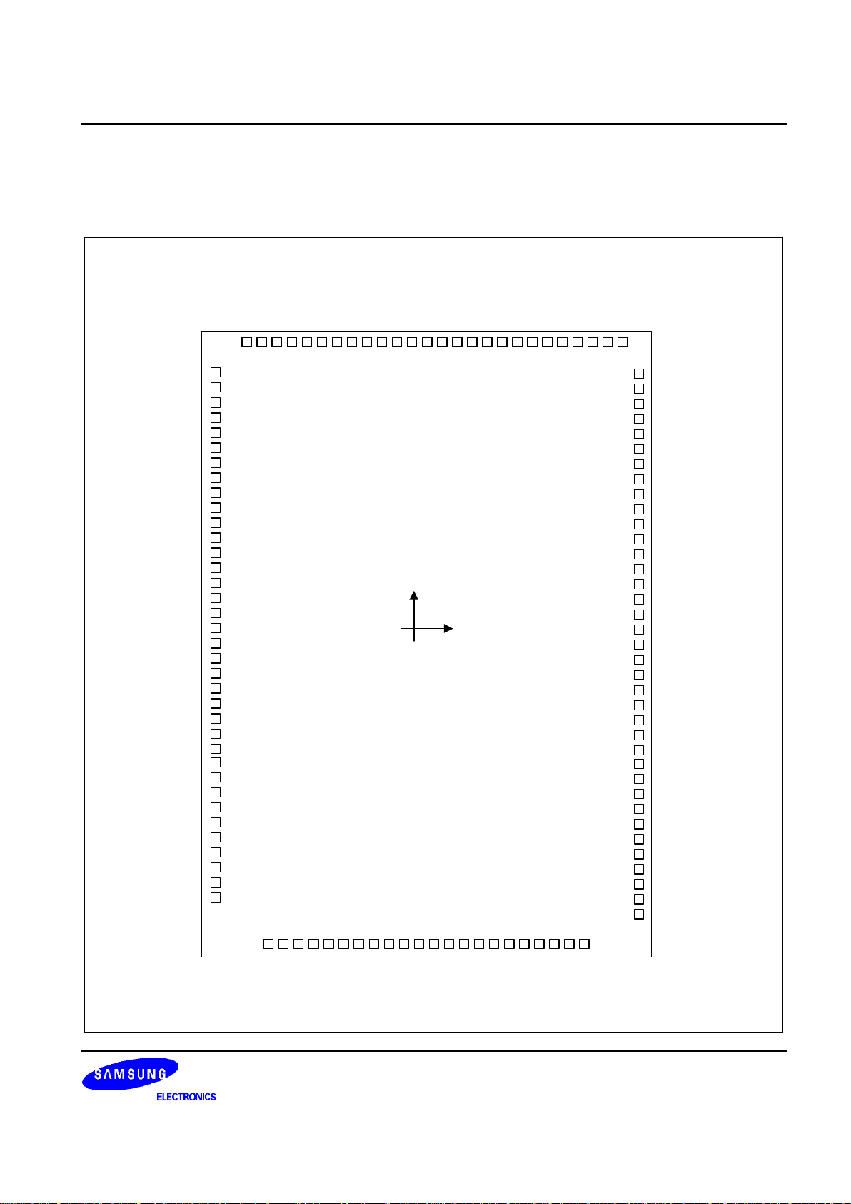
PAD CONFIGURATION
1) Normal Type PAD Configuration
SEG34
SEG35
SEG36
SEG37
SEG38
SEG39
SEG40
SEG41
SEG42
SEG43
SEG44
SEG45
SEG46
SEG47
SEG48
SEG49
SEG50
SEG51
SEG52
SEG53
SEG54
SEG55
SEG56
SEG57
SEG58
SEG59
128
127
126
125
124
123
122
121
120
119
118
117
116
115
114
113
112
111
110
109
108
107
106
105
104
103
S6A0070
Y
X
(0,0)
CHIP SIZE: 3920 x 5070
PAD SIZE: 100 x 100
UNIT: µm
424344454647484950515253545556575859606162
63
V1V2V3V4V5
CLK1
CLK2
M
D
RS
R/W
E
VDD
DB0
DB1
DB2
DB3
DB4
DB5
DB6
DB7
TEST
SEG33
SEG32
SEG31
SEG30
SEG29
SEG28
SEG27
SEG26
SEG25
SEG24
SEG23
SEG22
SEG21
SEG20
SEG19
SEG18
SEG17
SEG16
SEG15
SEG14
SEG13
SEG12
SEG11
SEG10
SEG9
SEG8
SEG7
SEG6
SEG5
SEG4
SEG3
SEG2
SEG1
VSS
OSC2
OSC1
2
3
4
5
6
7
8
9
10
11
12
13
14
15
16
17
18
19
20
21
22
23
24
25
26
27
28
29
30
31
32
33
34
35
36
37
102
101
100
99
98
97
96
95
94
93
92
91
90
89
88
87
86
85
84
83
82
81
80
79
78
77
76
75
74
73
72
71
70
69
68
67
66
SEG60
SEG61
SEG62
SEG63
SEG64
SEG65
SEG66
SEG67
SEG68
SEG69
SEG70
SEG71
SEG72
SEG73
SEG74
SEG75
SEG76
SEG77
SEG78
SEG79
SEG80
COM16
COM15
COM14
COM13
COM12
COM11
COM10
COM9
COM8
COM7
COM6
COM5
COM4
COM3
COM2
COM1

S6A0070 80 SEG / 16 COM DRIVER & CONTROLLER FOR DOT MATRIX LCD
6
2) Mirror Type PAD Configuration
SEG59
SEG58
SEG57
SEG56
SEG55
SEG54
SEG53
SEG52
SEG51
SEG50
SEG49
SEG48
SEG47
SEG46
SEG45
SEG44
SEG43
SEG42
SEG41
SEG40
SEG39
SEG38
SEG37
SEG36
SEG35
SEG34
128
127
126
125
124
123
122
121
120
119
118
117
116
115
114
113
112
111
110
109
108
107
106
105
104
103
SEG60
SEG61
SEG62
SEG63
SEG64
SEG65
SEG66
SEG67
SEG68
SEG69
SEG70
SEG71
SEG72
SEG73
SEG74
SEG75
SEG76
SEG77
SEG78
SEG79
SEG80
COM16
COM15
COM14
COM13
COM12
COM11
COM10
COM9
COM8
COM7
COM6
COM5
COM4
COM3
COM2
COM1
2
3
4
5
6
7
8
9
10
11
12
13
14
15
16
17
18
19
20
21
22
23
24
25
26
27
28
29
30
31
32
33
34
35
36
37
38
102
101
100
99
98
97
96
95
94
93
92
91
90
89
88
87
86
85
84
83
82
81
80
79
78
77
76
75
74
73
72
71
70
69
68
67
SEG33
SEG32
SEG31
SEG30
SEG29
SEG28
SEG27
SEG26
SEG25
SEG24
SEG23
SEG22
SEG21
SEG20
SEG19
SEG18
SEG17
SEG16
SEG15
SEG14
SEG13
SEG12
SEG11
SEG10
SEG9
SEG8
SEG7
SEG6
SEG5
SEG4
SEG3
SEG2
SEG1
VSS
OSC2
OSC1
S6A1070
414243444546474849505152535455565758596061
62
TEST
DB7
DB6
DB5
DB4
DB3
DB2
DB1
DB0
VDD
E
R/W
RS
D
M
CLK2
CLK1
V5V4V3V2V1
Y
X
(0,0)
CHIP SIZE: 3920 x 5070
PAD SIZE: 100 x 100
UNIT: mm

80 SEG / 16 COM DRIVER & CONTROLLER FOR DOT MATRIX LCD S6A0070
7
PAD CENTER COORDINATES
1) Normal Type PAD Coordinate (S6A0070)
COORDINATE COORDINATE COORDINATEPAD
NUM.
PAD
NAME
X Y
PAD
NUM.
PAD
NAME
X Y
PAD
NUM.
PAD
NAME
X Y
1 NC 44 V3 -905 -2369 87 SEG75 1794 294
2 SEG33 -1794 2169 45 V4 -780 -2369 88 SEG74 1794 419
3 SEG32 -1794 2044 46 V5 -655 -2369 89 SEG73 1794 544
4 SEG31 -1794 1919 47 CLK1 -530 -2369 90 SEG72 1794 669
5 SEG30 -1794 1794 48 CLK2 -405 -2369 91 SEG71 1794 794
6 SEG29 -1794 1669 49 M -280 -2369 92 SEG70 1794 919
7 SEG28 -1794 1544 50 D -155 -2369 93 SEG69 1794 1044
8 SEG27 -1794 1419 51 RS -30 -2369 94 SEG68 1794 1169
9 SEG26 -1794 1294 52 R/W 95 -2369 95 SEG67 1794 1294
10 SEG25 -1794 1169 53 E 220 -2369 96 SEG66 1794 1419
11 SEG24 -1794 1044 54 VDD 345 -2369 97 SEG65 1794 1544
12 SEG23 -1794 919 55 DB0 470 -2369 98 SEG64 1794 1669
13 SEG22 -1794 794 56 DB1 595 -2369 99 SEG63 1794 1794
14 SEG21 -1794 669 57 DB2 720 -2369 100 SEG62 1794 1919
15 SEG20 -1794 544 58 DB3 845 -2369 101 SEG61 1794 2044
16 SEG19 -1794 419 59 DB4 970 -2369 102 SEG60 1794 2169
17 SEG18 -1794 294 60 DB5 1095 -2369 103 SEG59 1563 2369
18 SEG17 -1794 169 61 DB6 1220 -2369 104 SEG58 1438 2369
19 SEG16 -1794 44 62 DB7 1345 -2369 105 SEG57 1313 2369
20 SEG15 -1794 -81 63 TEST 1470 -2369 106 SEG56 1188 2369
21 SEG14 -1794 -206 64 NC 107 SEG55 1063 2369
22 SEG13 -1794 -331 65 NC 108 SEG54 938 2369
23 SEG12 -1794 -456 66 COM1 1794 -2331 109 SEG53 813 2369
24 SEG11 -1794 -581 67 COM2 1794 -2206 110 SEG52 688 2369
25 SEG10 -1794 -706 68 COM3 1794 -2081 111 SEG51 563 2369
26 SEG9 -1794 -831 69 COM4 1794 -1956 112 SEG50 438 2369
27 SEG8 -1794 -956 70 COM5 1794 -1831 113 SEG49 313 2369
28 SEG7 -1794 -1081 71 COM6 1794 -1706 114 SEG48 188 2369
29 SEG6 -1794 -1206 72 COM7 1794 -1581 115 SEG47 63 2369
30 SEG5 -1794 -1331 73 COM8 1794 -1456 116 SEG46 -62 2369
S6A0070 80 SEG / 16 COM DRIVER & CONTROLLER FOR DOT MATRIX LCD
8
Normal Type Pad Coordinate (Continued)
COORDINATE COORDINATE COORDINATEPAD
NUM.
PAD
NAME
X Y
PAD
NUM.
PAD
NAME
X Y
PAD
NUM.
PAD
NAME
X Y
31 SEG4 -1794 -1456 74 COM9 1794 -1331 117 SEG45 -187 2369
32 SEG3 -1794 -1581 75 COM10 1794 -1206 118 SEG44 -312 2369
33 SEG2 -1794 -1706 76 COM11 1794 -1081 119 SEG43 -437 2369
34 SEG1 -1794 -1831 77 COM12 1794 -956 120 SEG42 -562 2369
35 VSS -1794 -1956 78 COM13 1794 -831 121 SEG41 -687 2369
36 OSC2 -1794 -2106 79 COM14 1794 -706 122 SEG40 -812 2369
37 OSC1 -1794 -2231 80 COM15 1794 -581 123 SEG39 -937 2369
38 NC 81 COM16 1794 -456 124 SEG38 -1062 2369
39 NC 82 SEG80 1794 -331 125 SEG37 -1187 2369
40 NC 83 SEG79 1794 -206 126 SEG36 -1312 2369
41 NC 84 SEG78 1794 -81 127 SEG35 -1437 2369
42 V1 -1155 -2369 85 SEG77 1794 44 128 SEG34 -1562 2369
43 V2 -1030 -2369 86 SEG76 1794 169
* “S6A0070” Marking: easy to find the PAD No. 98.
80 SEG / 16 COM DRIVER & CONTROLLER FOR DOT MATRIX LCD S6A0070
9
2) Mirror Type PAD Coordinate (S6A1070)
COORDINATE COORDINATE COORDINATEPAD
NUM.
PAD
NAME
X Y
PAD
NUM.
PAD
NAME
X Y
PAD
NUM.
PAD
NAME
X Y
1 NC 44 DB5 -1095 -2369 87 SEG18 1794 294
2 SEG60 -1794 2169 45 DB4 -970 -2369 88 SEG19 1794 419
3 SEG61 -1794 2044 46 DB3 -845 -2369 89 SEG20 1794 544
4 SEG62 -1794 1919 47 DB2 -720 -2369 90 SEG21 1794 669
5 SEG63 -1794 1794 48 DB1 -595 -2369 91 SEG22 1794 794
6 SEG64 -1794 1669 49 DB0 -470 -2369 92 SEG23 1794 919
7 SEG65 -1794 1544 50 VDD -345 -2369 93 SEG24 1794 1044
8 SEG66 -1794 1419 51 E -220 -2369 94 SEG25 1794 1169
9 SEG67 -1794 1294 52 RW -95 -2369 95 SEG26 1794 1294
10 SEG68 -1794 1169 53 RS 30 -2369 96 SEG27 1794 1419
11 SEG69 -1794 1044 54 D 155 -2369 97 SEG28 1794 1544
12 SEG70 -1794 919 55 M 280 -2369 98 SEG29 1794 1669
13 SEG71 -1794 794 56 CLK2 405 -2369 99 SEG30 1794 1794
14 SEG72 -1794 669 57 CLK1 530 -2369 100 SEG31 1794 1919
15 SEG73 -1794 544 58 V5 655 -2369 101 SEG32 1794 2044
16 SEG74 -1794 419 59 V4 780 -2369 102 SEG33 1794 2169
17 SEG75 -1794 294 60 V3 905 -2369 103 SEG34 1562 2369
18 SEG76 -1794 169 61 V2 1030 -2369 104 SEG35 1437 2369
19 SEG77 -1794 44 62 V1 1155 -2369 105 SEG36 1312 2369
20 SEG78 -1794 -81 63 NC 106 SEG37 1187 2369
21 SEG79 -1794 -206 64 NC 107 SEG38 1062 2369
22 SEG80 -1794 -331 65 NC 108 SEG39 937 2369
23 C16 -1794 -456 66 NC 109 SEG40 812 2369
24 C15 -1794 -581 67 OSC1 1794 -2231 110 SEG41 687 2369
25 C14 -1794 -706 68 PSC2 1794 -2106 111 SEG42 562 2369
26 C13 -1794 -831 69 VSS 1794 -1956 112 SEG43 437 2369
27 C12 -1794 -956 70 SEG1 1794 -1831 113 SEG44 312 2369
28 C11 -1794 -1081 71 SEG2 1794 -1706 114 SEG45 187 2369
29 C10 -1794 -1206 72 SEG3 1794 -1581 115 SEG46 62 2369
30 C9 -1794 -1331 73 SEG4 1794 -1456 116 SEG47 -63 2369
31 C8 -1794 -1456 74 SEG5 1794 -1331 117 SEG48 -188 2369
32 C7 -1794 -1581 75 SEG6 1794 -1206 118 SEG49 -313 2369
33 C6 -1794 -1706 76 SEG7 1794 -1081 119 SEG50 -438 2369
S6A0070 80 SEG / 16 COM DRIVER & CONTROLLER FOR DOT MATRIX LCD
10
Mirror Type Pad Coordinate (Continued)
COORDINATE COORDINATE COORDINATEPAD
NUM.
PAD
NAME
X Y
PAD
NUM.
PAD
NAME
X Y
PAD
NUM.
PAD
NAME
X Y
34 COM5 -1794 -1831 77 SEG8 1794 -956 120 SEG51 -563 2369
35 COM4 -1794 -1956 78 SEG9 1794 -831 121 SEG52 -688 2369
36 COM3 -1794 -2081 79 SEG10 1794 -706 122 SEG53 -813 2369
37 COM2 -1794 -2206 80 SEG11 1794 -581 123 SEG54 -938 2369
38 COM1 -1794 -2331 81 SEG12 1794 -456 124 SEG55 -1063 2369
39 NC 82 SEG13 1794 -331 125 SEG56 -1188 2369
40 NC 83 SEG14 1794 -206 126 SEG57 -1313 2369
41 TEST -1470 -2369 84 SEG15 1794 -81 127 SEG58 -1438 2369
42 DB7 -1345 -2369 85 SEG16 1794 44 128 SEG59 -1563 2369
43 DB6 -1220 -2369 86 SEG17 1794 169
* “S6A1070” Marking: easy to find the PAD No. 12.
80 SEG / 16 COM DRIVER & CONTROLLER FOR DOT MATRIX LCD S6A0070
11
PIN DESCRIPTION
Pad (No)
(normal/mirror)
I/O Name Description Interface
VDD(54/50)
for logical circuit (+3V, +5V)
VSS(35, 69)
Power supply
0V (GND)
V1-V5
(42-46/62-58)
Power supply
Bias voltage level for LCD driving
Power
supply
SEG1-SEG80
(34-2, 128-82/
70-128, 2-28
Output Segment output Segment signal output for LCD driving LCD
COM1-COM16
(66-81/38-23)
Output Common output Common signal output for LCD driving LCD
OSC1, OSC2
(37, 36/67, 68)
Input
(OSC1)
Output
(OSC2)
Oscillator
When using internal oscillator, connect
external Rf resistor.
If external clock is used, connect it to
OSC1.
Extension
register/
oscillator
(OSC1)
CLK1, CLK2
(47, 48/57, 56)
Output
Extension driver latch
(CLK1)/Shift (CLK2)
clock
Each outputs extension driver latch clock
and extension driver shift clock
Extension
driver
M (49/55) Output
Alternated signal for
LCD driver output
Outputs the alternating signal to convert
LCD driver waveform to AC.
Extension
driver
D (50/54) Output Display data interface
Output extension driver data (the 41st
dot's data)
Extension
driver
RS (51/53) Input Register select
Used s register selection input.
When RS = 1, Data register is selected.
When RS = 0, Instruction register is
selected
MPU
RW (52/52) Input Read/Write
Used as read/write selection input.
When RW = 1, read operation.
When RW = 0, write operation.
MPU
E (53/51) Input Read/Write Enable Used as read. Write enable signal. MPU
DB0-DB3
(55-58/49-46)
Input/
Output
Data bus 0-3
When 8-bit bus mode, used as low order
bidirectional data bus. During 4-bit bus
mode open these pins.
MPU
DB4-DB7
(59-62/45-42)
Input/
Output
Data bus 4-7
When 8-bit bus mode, used as high
order bidirectional data bus. In case of 4bit bus mode, used as both high and low
order.
DB7 used for Busy Flag output.
MPU
TEST(63/41) Input Test pin This pin must be fixed to VDD or open. -
S6A0070 80 SEG / 16 COM DRIVER & CONTROLLER FOR DOT MATRIX LCD
12
FUNCTION DESCRIPTION
System Interface
This chip has both kinds of interface type with MPU: 4-bit bus and 8-bits bus. 4-bit bus and 8-bit bus are selected
by the DL bit in the instruction register.
During read or write operation, two 8-bit registers are used. One is the data register (DR), and the other is the
instruction register (IR).
The data register (DR) is used as a temporary data storage place for being written into or read from
DRAM/CGRAM . Target RAM is selected by RAM address setting instruction. Each internal operation, reading
from or writing into RAM, is done automatically. After MPU reads DR data, the data in the next DDRAM/CGRAM
address is transferred into DR automatically. Also, after MPU writes data to DR, the data in DR is transferred into
DDRAM/CGRAM automatically.
The instruction register (IR) is used only to store instruction codes transferred from MPU. MPU cannot use it to
read instruction data.
To select a register, use RS input pin in 4-bit/8-bit bus mode.
Table 1. Various Kinds of Operations to RS and R/W bits.
RS R/W Operation
0 0 Instruction Write operation (MPU writes instruction code into IR)
0 1 Read Busy flag (DB7) and address counter (DB0 - DB7)
1 0 Data Write operation (MPU writes data into DR)
1 1 Data Read operation (MPU reads data into DR)
Busy Flag (BF)
When BF = 1, it indicates that the internal operation is being processed. So during this time the next instruction
cannot be accepted. BF can be read, when RS = 0, and R/W = 1. (Read Instruction Operation), through DB7
port. Before executing the next instruction, be sure that BF is not 1.
80 SEG / 16 COM DRIVER & CONTROLLER FOR DOT MATRIX LCD S6A0070
13
Address Counter (AC)
The Address Counter (AC) stores DDRAM/CGRAM addresses, transferred from IR. After writing into (reading
from) DDRAM/CGRAM. AC is automatically increased (decreased) by 1. When RS = 0 and R/W = 1, AC can be
read through ports DB0 - DB6.
Display Data RAM (DDRAM)
DDRAM stores display data of maximum 80 x 8 bits (80 characteristics). DDRAM address is set in the address
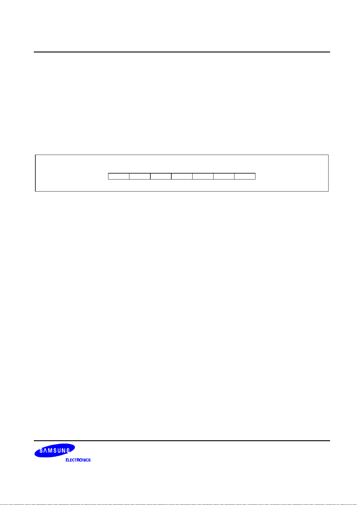
counter (AC) as a hexadecimal number. (Refer to fig-1).
AC6
MSB LSB
AC5 AC4 AC3 AC2 AC1 AC0
Figure 1. DDRAM Address
1) 1-line Display
In the case of a 1-line display, the address range of DDRAM is 00H - 04H. An Extension driver will be used.
Figure 2 shows the example when a 40-segment extension driver is added.
2) 2-line Display
In the case of a 2-line display, the address range of DDRAM is 00H - 27H and 40H - 67H. An Extension driver will
be used. Figure 3 shows the example a 40 segment extension driver is added.
 Loading...