

Samsung S6A0090 Datasheet
64 SEG / 26 COM DRIVER & CONTROLLER FOR STN LCD
S6A0090
written permission of LCD Driver IC Team.
June. 2000.
Prepared by: Weon-seek, Kang
Ver. 0.2
Contents in this document are subject to change without notice. No part of this document may be reproduced
or transmitted in any form or by any means, electronic or mechanical, for any purpose, without the express
k2w2@samsung.co.kr
S6A0090 64 SEG / 26 COM DRIVER & CONTROLLER FOR STN LCD
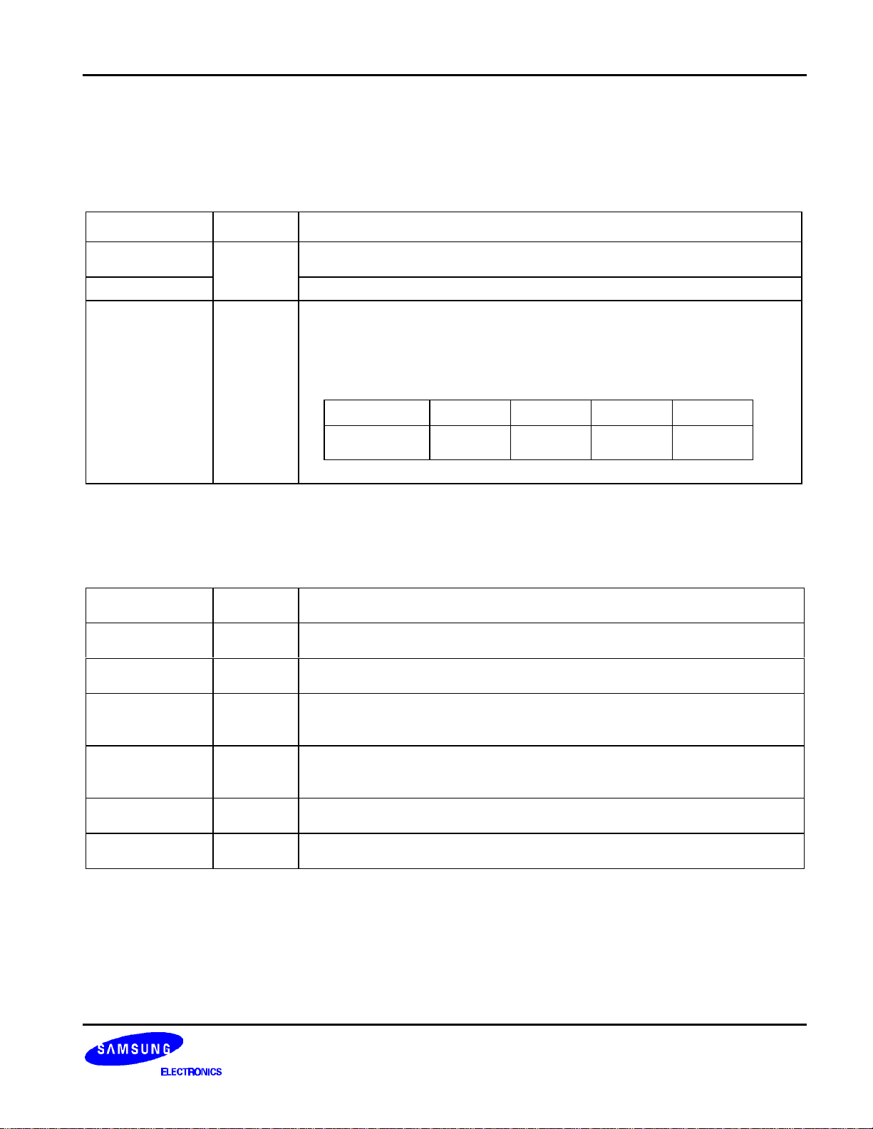
S6A0090 Specification Revision History
Version Content Date
0.0 Original Jun.1998
0.1 KS0090 à KS0090B, add ILB key Apr.1999
0.2 Add power ON / OFF sequence Apr.1999
Inspection Jun.2000
2
64 SEG / 26 COM DRIVER & CONTROLLER FOR STN LCD S6A0090
CONTENTS
INTRODUCTION ................................................................................................................................................. 1
FEATURES.........................................................................................................................................................1
BLOCK DIAGRAM..............................................................................................................................................3
PAD CONFIGURATION ...................................................................................................................................... 4
PAD CENTER COORDINATES ........................................................................................................................... 5
PIN DESCRIPTION ............................................................................................................................................. 7
POWER SUPPLY ..........................................................................................................................................7
LCD DRIVER SUPPLY..................................................................................................................................7
SYSTEM CONTROL .....................................................................................................................................8
MPU INTERFACE.........................................................................................................................................8
LCD DRIVER OUTPUTS (DYNAMIC)............................................................................................................9
LCD DRIVER OUTPUTS (STATIC) ...............................................................................................................9
FUNCTION DESCRIPTION ............................................................................................................................... 10
SYSTEM INTERFACE.................................................................................................................................10
ADDRESS COUNTER (AC).........................................................................................................................14
DISPLAY DATA RAM (DDRAM)..................................................................................................................14
CHARACTER GENERATOR ROM (CGROM) .............................................................................................15
CHARACTER GENERATOR RAM (CGRAM)..............................................................................................16
SEGMENT ICON RAM (ICONRAM) ............................................................................................................17
STATIC ICON RAM (SI) .............................................................................................................................. 18
SEGMENTS FOR SIGNAL DISPLAY (FS)................................................................................................... 18
LOW POWER CONSUMPTION MODE.......................................................................................................19
LCD DRIVER CIRCUIT ...............................................................................................................................19
INSTRUCTION DESCRIPTION.......................................................................................................................... 20
INITIALIZING & POWER SAVE MODE SETUP................................................................................................. 26
HARDWARE RESET ...................................................................................................................................26
INITIALIZING AND POWER SAVE MODE SETUP......................................................................................27
LCD DRIVING POWER SUPPLY CIRCUIT ....................................................................................................... 30
VOLTAGE CONVERTER ............................................................................................................................31
VOLTAGE REGULATOR.............................................................................................................................32
VOLTAGE GENERATOR CIRCUIT.............................................................................................................35
REFERENCE APPLICATIONS.......................................................................................................................... 36
MPU INTERFACE.......................................................................................................................................36
APPLICATION INFORMATION FOR LCD PANEL.......................................................................................38
FRAME FREQUENCY.................................................................................................................................42
MAXIMUM ABSOLUTE RATINGS .................................................................................................................... 43
ELECTRICAL CHARACTERISTICS.................................................................................................................. 44
DC CHARACTERISTICS .............................................................................................................................44
AC CHARACTERISTICS.............................................................................................................................47
3

64 SEG / 26 COM DRIVER & CONTROLLER FOR STN LCD S6A0090
INTRODUCTION
The S6A0090 is an LCD driver and controller LSI for liquid crystal dot matrix character display systems. It can
display 2 or 3 lines of 12 characters with 5 x 8 dots format. It is capable of interfacing with various
microprocessors, supporting the 4-bit and 8-bit parallel mode and the clock synchronized serial mode. Voltage
converter (2 or 3 times), voltage regulator, divider resistor and voltage follower OP AMP are built in the IC and a
low operation current of 50µA is achieved. The slim shape of the chip makes it suitable for the COG module
application and TCP. The S6A0090 is an ideal solution for display on portable equipment such as cellular phones.
FEATURES
Driver Outputs
- Common outputs: 26 common
- Segment outputs: 64 segment
- Icons: 128 horizontal icons, 24 x 4 vertical icons, 5 static icons
Applicable Panel Size
Display size Duty Contents of outputs
2-line x 12 characters 1/18 (12 characters + 4 segments for signal) x 2 + 128 icons + 5 static icons
3-line x 12 characters 1/26 (12 characters + 4 segments for signal) x 3 + 128 icons + 5 static icons
Internal Memory
- Character Generator ROM (CGROM): 10,240 bits (256 characters x 5 x 8 dots)
- Character Generator RAM (CGRAM): 160 bits (4 characters x 5 x 8 dots)
- Display Data RAM (DDRAM): 288 bits (12 characters x 3 lines x 8 bits)
- Segment Icon RAM (ICONRAM): 224 bits (12 x 2 x 5 bits + 2 x 4 bits + 24 x 4 bits)
MPU Interface
- No busy MPU interface (no busy check or no execution waiting time)
- 8-bit parallel interface mode: 68-series and 80-series are available
- 4-bit parallel interface mode: 68-series and 80-series are available
- Serial interface mode: 4 pins clock synchronized serial interface
Function Set
- Various instructions set: display control, power save, power control, function set, etc.
- COM / SEG bi-directional function (4 types of LCD application available)
- Hardware reset (RES pin)
Built-in Analog Circuit
- On-chip oscillator with an internal resistor or external clock input
- Electronic volume for contrast control (32 or 64 steps)
- Voltage converter (2 or 3 times) / voltage regulator / voltage follower and bias circuit
1

S6A0090 64 SEG / 26 COM DRIVER & CONTROLLER FOR STN LCD
Low Power Consumption
- 80 µA Max. : in normal mode for normal display operation
- 10 µA Max. : in standby mode for displaying static icon
- 5 µA Max. : in sleep mode when display is turned OFF
Operating Voltage Range
- Power supply voltage (VDD): 2.4 to 5.5 V
- LCD driving voltage (VLCD = V0 - VSS): 11.0 V (positive process)
Package Type
- Gold bumped chip or TCP
2
64 SEG / 26 COM DRIVER & CONTROLLER FOR STN LCD S6A0090
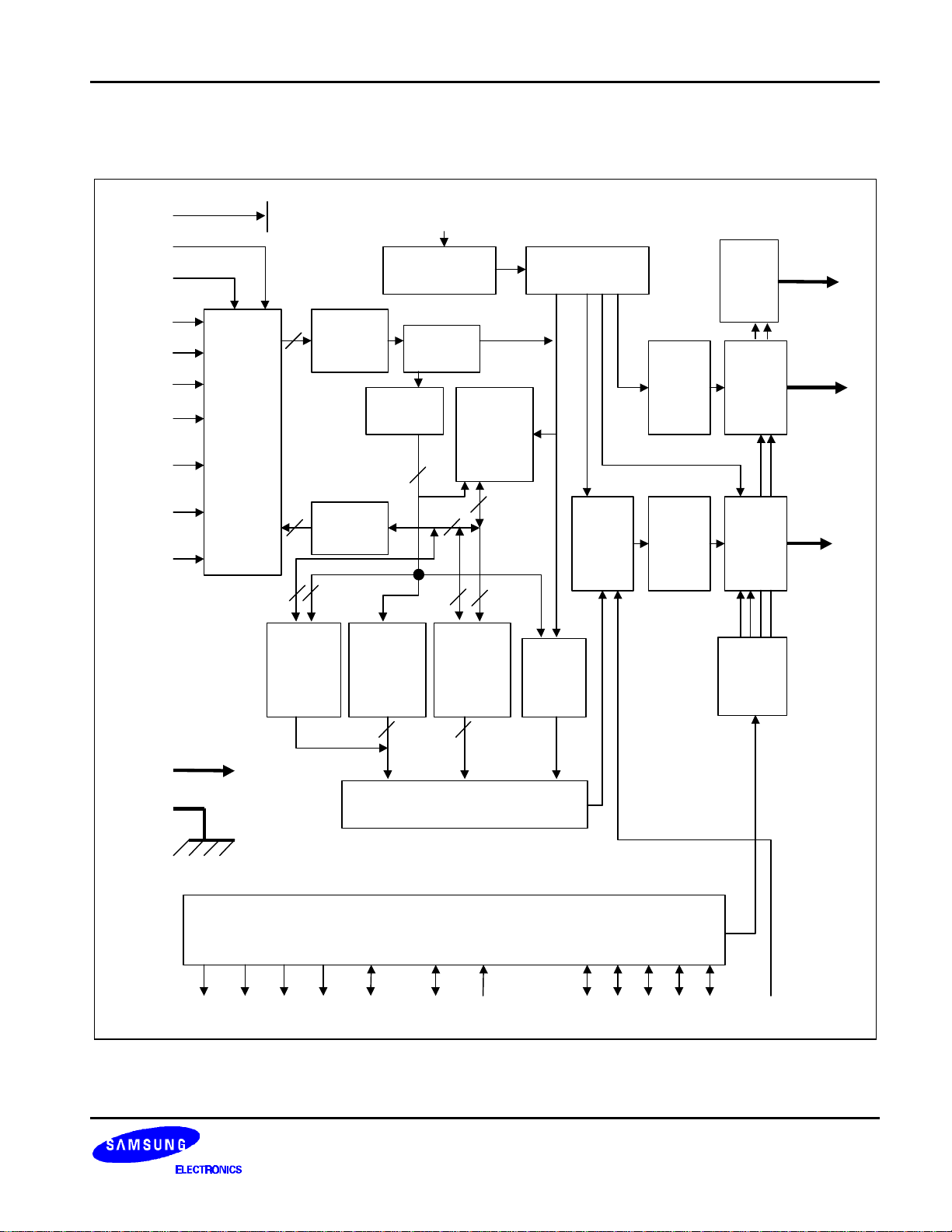
BLOCK DIAGRAM
RES
PS
IF
CSB
RS
E
DB7
(SI)
DB6
(SCL)
DB5~
DB4
DB3~
DB0
Parallel
Interface
4-bit/8-bit
Serial
Interface
Input Buffer
Instruction
8
8
8
7
Icon RAM
(ICONRAM)
224 bits
Register
(IR)
Data
Register
(DR)
Character
Generator
(CGRAM)
Address
Counter
RAM
32 bytes
CK
Instruction
Decoder
7
8
8
Character
Generator
ROM
(CGROM)
10240 bits
Display
Data RAM
(DDRAM)
36x8 bits
8
8
Timing GeneratorOscillator
Cursor &
Blink
Controller
64 bits
Shift
Register
26 bits
Shift
Register
64 bits
Latch
Circuit
Static
Driver
Common
Driver
Segment
Driver
LCD
Driver
Voltage
Selector
COMSA
SEGSA~E
COM1~
COM24
COM S1
COM S2
SEG1~
SEG60
SEGS1,2
4,5
VDD
GND
(VSS)
5 5
Segment Data Conversion
LCD Driving Power Circuit
Voltage Converter Voltage Regulator Voltage Follower &
Bias Resistor
CAP1+ CAP1- CAP2+ CAP2- VOUT V0 VR V0 V1 V2 V3 V4 BID
Figure 1. Block Diagram
3
S6A0090 64 SEG / 26 COM DRIVER & CONTROLLER FOR STN LCD
.....
X
188
.....
30
µ
m
30
µ
m
30
µ
m
60
µ
m
30
µ
m
42
µ
m
108
µ
m
42
µ
m
108
µ
m
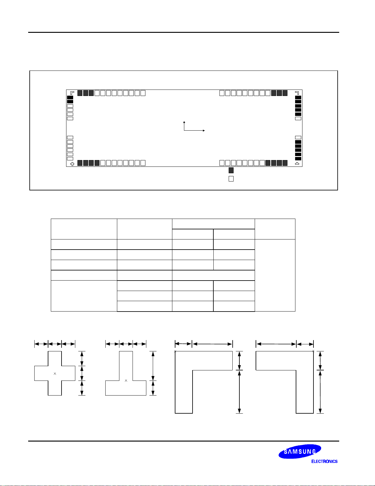
PAD CONFIGURATION
1
...........................
Y
(0,0)
...........................
Figure 2. Pad Configuration
Table 1. S6A0090 Pad Dimensions
Item
Pad No.
(location)
Chip size - 7410 2470
Pad size 1 to 188 60 118
Bumped pad size 1 to 188 56 114
Bumped pad height 1 to 188
Left, right top 150 150
Left bottom 90 90Align key size
Right bottom 90 90
Size
X Y
17 ± 1.5
DUMMY PAD
PAD
Unit
µm
COG Align Key Coordinate ILB Align Key Coordinate
30µm 30µm 30µm
(-3479, -1110)
4
30µm 30µm 30µm
(+3479, -1125)
42µm 108µm
(-3535, +1119)
42µm108µm
(+3535, +1119)
64 SEG / 26 COM DRIVER & CONTROLLER FOR STN LCD S6A0090
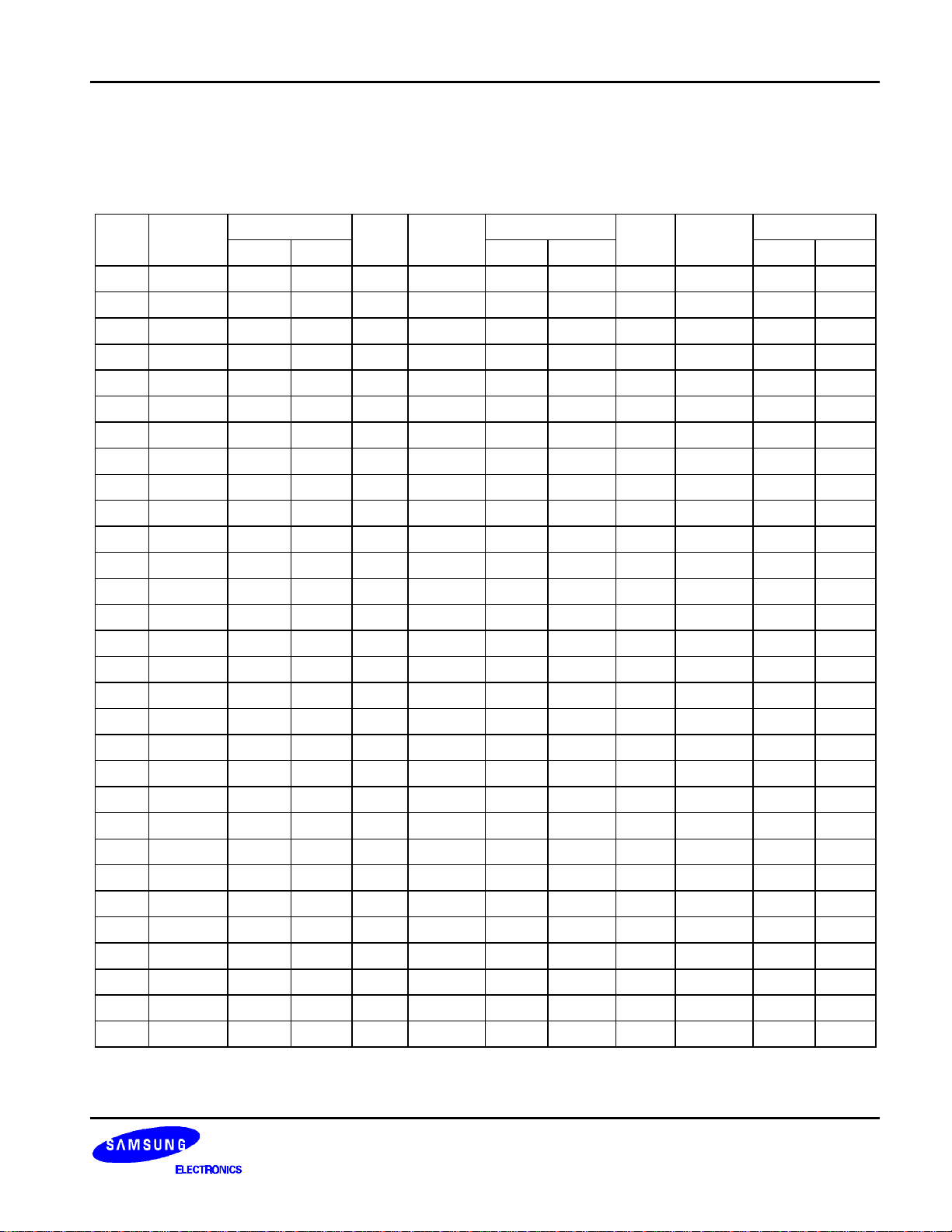
PAD CENTER COORDINATES
Table 2. Pad Center Coordinates
[Unit: µm]
Pad
No.
1 DUMMY -3540 880 31 DB5 -2430 -1111 61 CAP2- 270 -1111
2 DUMMY -3540 790 32 DB4 -2340 -1111 62 CAP2- 360 -1111
3 COM21 -3540 700 33 DB3 -2250 -1111 63 CAP2- 450 -1111
4 COM20 -3540 610 34 DB2 -2160 -1111 64 CAP2- 540 -1111
5 COM19 -3540 520 35 DB1 -2070 -1111 65 CAP2+ 630 -1111
6 COM18 -3540 430 36 DB0 -1980 -1111 66 CAP2+ 720 -1111
7 COM17 -3540 340 37 VDD -1890 -1111 67 CAP2+ 810 -1111
8 COM16 -3540 250 38 VDD -1800 -1111 68 CAP2+ 900 -1111
9 COM15 -3540 160 39 VDD -1710 -1111 69 CAP1- 990 -1111
10 COM14 -3540 70 40 VSS -1620 -1111 70 CAP1- 1080 -1111
11 COM13 -3540 -20 41 VSS -1530 -1111 71 CAP1- 1170 -1111
12 COM12 -3540 -110 42 VSS -1440 -1111 72 CAP1- 1260 -1111
13 COM11 -3540 -200 43 V4 -1350 -1111 73 CAP1+ 1350 -1111
14 COM10 -3540 -290 44 V4 -1260 -1111 74 CAP1+ 1440 -1111
15 COM9 -3540 -380 45 V3 -1170 -1111 75 CAP1+ 1530 -1111
16 COMS2 -3540 -470 46 V3 -1080 -1111 76 CAP1+ 1620 -1111
17 SEGSA -3540 -560 47 V2 -990 -1111 77 VSS 1710 -1111
18 SEGSB -3540 -650 48 V2 -900 -1111 78 VSS 1800 -1111
19 SEGSC -3540 -740 49 V1 -810 -1111 79 VSS 1890 -1111
20 SEGSD -3540 -830 50 V1 -720 -1111 80 BID 1980 -1111
21 SEGSE -3540 -920 51 V0 -630 -1111 81 VDD 2070 -1111
22 DUMMY -3240 -1111 52 V0 -540 -1111 82 VDD 2160 -1111
23 DUMMY -3150 -1111 53 V0 -450 -1111 83 VDD 2250 -1111
24 DUMMY -3060 -1111 54 V0 -360 -1111 84 CK 2340 -1111
25 DUMMY -2970 -1111 55 VR -270 -1111 85 VDD 2430 -1111
26 RS -2880 -1111 56 VR -180 -1111 86 PS 2520 -1111
27 E -2790 -1111 57 VOUT -90 -1111 87 IF 2610 -1111
28 CSB -2700 -1111 58 VOUT 0 -1111 88 RES 2700 -1111
29 DB7 -2610 -1111 59 VOUT 90 -1111 89 VDD 2790 -1111
30 DB6 -2520 -1111 60 VOUT 180 -1111 90 VDD 2880 -1111
Pad
Name
Coordinate Coordinate Coordinate
X Y
Pad
No.
Pad
Name
X Y
Pad
No.
Pad
Name
X Y
5
S6A0090 64 SEG / 26 COM DRIVER & CONTROLLER FOR STN LCD
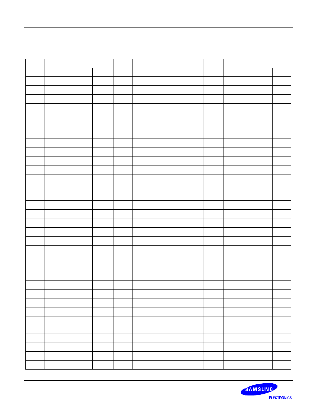
Table 2. Pad Center Coordinates (Continued)
[Unit: um]
Pad
No.
Pad
Name
Coordinate Coordinate Coordinate
X Y
Pad
No.
Pad
Name
X Y
Pad
No.
Pad
Name
X Y
91 DUMMY 2970 -1111 124 SEG4 2520 1070 157 SEG37 -450 1070
92 DUMMY 3060 -1111 125 SEG5 2430 1070 158 SEG38 -540 1070
93 DUMMY 3150 -1111 126 SEG6 2340 1070 159 SEG39 -630 1070
94 DUMMY 3240 -1111 127 SEG7 2250 1070 160 SEG40 -720 1070
95 DUMMY 3540 -920 128 SEG8 2160 1070 161 SEG41 -810 1070
96 DUMMY 3540 -830 129 SEG9 2070 1070 162 SEG42 -900 1070
97 DUMMY 3540 -740 130 SEG10 1980 1070 163 SEG43 -990 1070
98 DUMMY 3540 -650 131 SEG11 1890 1070 164 SEG44 -1080 1070
99 DUMMY 3540 -560 132 SEG12 1800 1070 165 SEG45 -1170 1070
100 COMSA 3540 -470 133 SEG13 1710 1070 166 SEG46 -1260 1070
101 COMS1 3540 -380 134 SEG14 1620 1070 167 SEG47 -1350 1070
102 COM1 3540 -290 135 SEG15 1530 1070 168 SEG48 -1440 1070
103 COM2 3540 -200 136 SEG16 1440 1070 169 SEG49 -1530 1070
104 COM3 3540 -110 137 SEG17 1350 1070 170 SEG50 -1620 1070
105 COM4 3540 -20 138 SEG18 1260 1070 171 SEG51 -1710 1070
106 COM5 3540 70 139 SEG19 1170 1070 172 SEG52 -1800 1070
107 COM6 3540 160 140 SEG20 1080 1070 173 SEG53 -1890 1070
108 COM7 3540 250 141 SEG21 990 1070 174 SEG54 -1980 1070
109 COM8 3540 340 142 SEG22 900 1070 175 SEG55 -2070 1070
110 COMS1 3540 430 143 SEG23 810 1070 176 SEG56 -2160 1070
111 DUMMY 3540 520 144 SEG24 720 1070 177 SEG57 -2250 1070
112 DUMMY 3540 610 145 SEG25 630 1070 178 SEG58 -2340 1070
113 DUMMY 3540 700 146 SEG26 540 1070 179 SEG59 -2430 1070
114 DUMMY 3540 790 147 SEG27 450 1070 180 SEG60 -2520 1070
115 DUMMY 3540 880 148 SEG28 360 1070 181 SEGS4 -2610 1070
116 DUMMY 3240 1070 149 SEG29 270 1070 182 SEGS5 -2700 1070
117 DUMMY 3150 1070 150 SEG30 180 1070 183 COM24 -2790 1070
118 DUMMY 3060 1070 151 SEG31 90 1070 184 COM23 -2880 1070
119 SEGS1 2970 1070 152 SEG32 0 1070 185 COM22 -2970 1070
120 SEGS2 2880 1070 153 SEG33 -90 1070 186 DUMMY -3060 1070
121 SEG1 2790 1070 154 SEG34 -180 1070 187 DUMMY -3150 1070
122 SEG2 2700 1070 155 SEG35 -270 1070 188 DUMMY -3240 1070
123 SEG3 2610 1070 156 SEG36 -360 1070
* NOTE: The COMS1 has two terminals (#101, #110), and these two COMS1 are the same signal at the same time
6
64 SEG / 26 COM DRIVER & CONTROLLER FOR STN LCD S6A0090
PIN DESCRIPTION
POWER SUPPLY
Table 3. Pin Description
Name I/O Description
VDD
VSS
V0
V1
V2
V3
V4
Power
I/O
LCD DRIVER SUPPLY
Name I/O Description
CAP1+ O
CAP1- O
CAP2+ O
CAP2– O
VOUT I/O
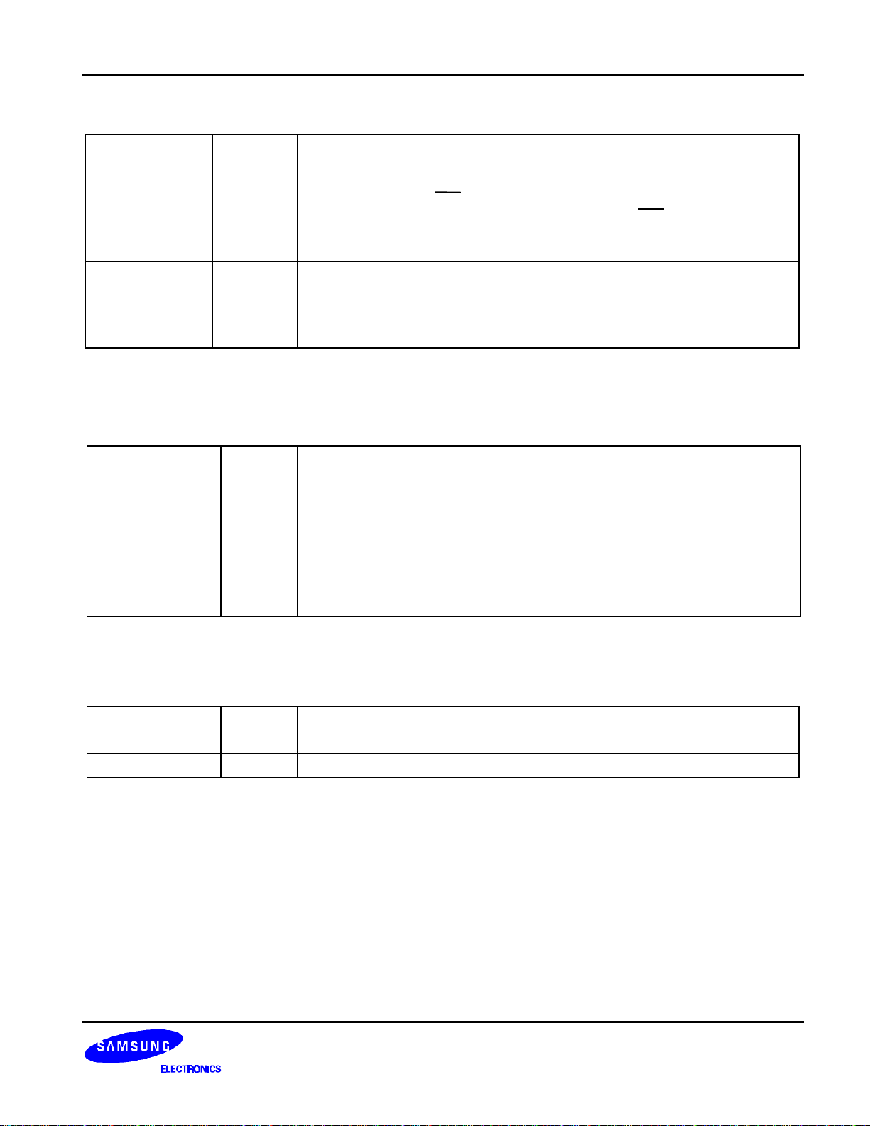
VR I
Power supply
Connect to MPU power supply pin
0V (GND)
Bias voltage level for LCD driving
Voltages should have the following relationship;
V0 ≥ V1 ≥ V2 ≥ V3 ≥ V4 ≥ VSS
When the built-in power circuit is on, the following voltages are given to pins V1
to V4 by internal 1/5 bias resistors are used.
LCD bias V1 V2 V3 V4
(1/5) bias (4/5) x V0 (3/5) x V0 (2/5) x V0 (1/5) x V0
Table 3. Pin Description (continued)
Capacitor 1+ connecting pin for the internal voltage converter
This pin connects the capacitor with CAP1-.
Capacitor1- connecting pin for the internal voltage converter
This pin connects the capacitor with CAP1+.
Capacitor 2+ connecting pin for the internal voltage converter
When VOUT is 2 times boosting, this pin connects the capacitor with VDD,
when 3 times boosting, this pin connects the capacitor with CAP2Capacitor2- connecting pin for the internal voltage converter
When VOUT is 2 times boosting, this pin is not used, when 3 times boosting,
this pin connects the capacitor with CAP2+
2 or 3 times DC/DC voltage converter output
This pin connects a capacitor with VDD pin.
Voltage adjust pin
This pin gives a voltage between V0 and VSS by resistance-division of voltage.
7
S6A0090 64 SEG / 26 COM DRIVER & CONTROLLER FOR STN LCD
SYSTEM CONTROL
Table 3. Pin Description (continued)
Name I/O Description
External clock input pin
CK I
PS I
IF I
BID I
It must be fixed to "High" when the internal oscillation circuit is used.
In the external clock mode, it is used as external clock input pin.
Parallel / serial selection pin
When PS = "Low": serial mode
When PS = "High": 4-bit/8-bit bus mode
Interface data length selection pin for parallel data input
When PS = "Low"
IF = "Low " or "High": serial interface mode
When PS = “High”
IF = "Low": 4-bit bus mode
IF = "High": 8-bit bus mode
SEG direction selection pin
When BID = "Low";
SEGS1 → SEGS2 → SEG1 → ...... → SEG60 → SEGS4 → SEGS5
When BID = "High";
SEGS5 → SEGS4 → SEG60 → ...... → SEG1 → SEGS2 → SEGS1
MPU INTERFACE
Name I/O Description
RES I
CSB I
RS I
Table 3. Pin Description (continued)
Initialization is performed by edge sensing of the RES signal.
An interface type for the 68/80 series MPU is selected by input level after
initialization.
When RES = "Low": 68 series MPU
When RES = "High": 80 series MPU
Chip selection pin
When CSB = "Low": selected
When CSB = "High": not selected
Register selection pin
When RS = "Low": instruction register
When RS = "High": data register
8
64 SEG / 26 COM DRIVER & CONTROLLER FOR STN LCD S6A0090
Table 3. Pin Description (Continued)
Name I/O Description
In 80 series MPU interface mode, active "Low".
This pin connects the WR pin of the 80 series MPU.
E I
DB0 to DB3
DB4 to DB5
DB6 (SCL)
DB7 (SI)
I
The signal on the data bus is fetched at the rise of the WR signal.
In 68 series MPU interface mode, active "High".
This pin becomes an enable clock input of the 68 series MPU.
When in 8-bit interface mode, DB0 to DB7 are used as input data bus pin
In the 4-bit bus mode, only DB4 to DB7 are used as data input pin and DB0 to
DB3 are not used.
In the serial mode, DB6 (SCL) is used as serial clock input pin, DB7 (SI) is
used as serial data input pin and the others are not used.
LCD DRIVER OUTPUTS (DYNAMIC)
Table 3. Pin Description
Name I/O Description
COM1 to COM24 O
COMS1, COMS2 O
SEG1 to SEG60 O
SEGS1, SEGS2
SEGS4, SEGS5
O
Common signal output for character display
Common signal output for icon display
The COMS1 has two terminals and these two COMS1 are the same signal at
the same time.
Segment signal output for character display
Segment signal output for vertical icon display
LCD DRIVER OUTPUTS (STATIC)
Table 3. Pin Description (continued)
Name I/O Description
COMSA O Static common signal output for static icon display
SEGSA, B, C, D, E O Static segment signal output for static icon display
* NOTE: DUMMY - These pins should be opened (floated).
9
S6A0090 64 SEG / 26 COM DRIVER & CONTROLLER FOR STN LCD
FUNCTION DESCRIPTION
SYSTEM INTERFACE
S6A0090 has two kinds of interface type with MPU: bus mode and serial mode. Bus mode or serial mode is
selected by PS pin. In bus mode, 4-bit bus or 8-bit bus is selected by IF pin, and 68 series MPU or 80 series MPU
is selected by RES pin.
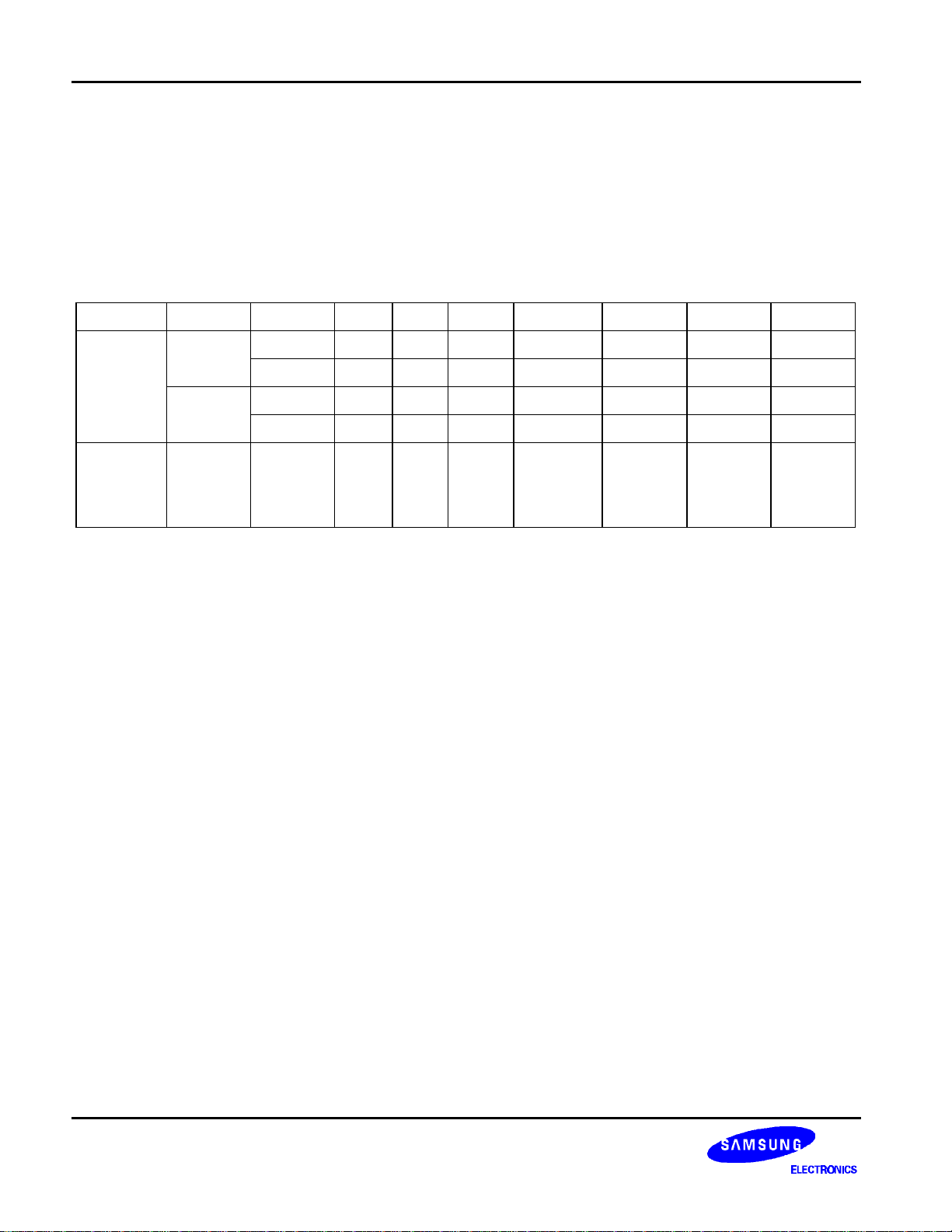
Table 4. Various kinds of MPU interface according to PS, RES and IF
PS RES IF CSB RS E DB0 to 3 DB4 to 5 DB6 DB7
80 series
Bus
mode (H)
Serial
mode (L)
"*": Don't care ("High", "Low" or "Open"), (H)/(L): fixed "High"(VDD) or "Low"(VSS)
PS: "High" = bus mode, "Low" = serial mode
RES: "High" = 80-series MPU, "Low" = 68-series MPU
IF: "High" = 8-bit mode, "Low" = 4-bit mode (PS: "High")
CSB: "High" = chip is not selected, "Low" = chip is selected
RS: "High" = data register, “Low" = instruction register
E: 80-series active "Low", 68-series active "High"
SCL (DB6): serial clock input
SI (DB7): serial data input
Interface with MPU in Parallel Mode (PS = "High")
During writing operation, two 8-bit registers, data register (DR) and instruction register (IR), are used. The data
register (DR) is used as temporary data storage place for being written into DDRAM / CGRAM / ICONRAM, and
one of these RAMs is selected by RAM address setting instruction. The Instruction register (IR) is used only to
store instruction code transferred from MPU. To select DR or IR register, RS input pin is used in bus mode or
serial mode. In 4-bit bus mode, it is needed to transfer 4-bit data (DB4 to DB7) by two times. The high order bits
(for 8-bit mode DB4 to DB7) are transferred before the low order bits (for 8-bit mode DB0 to DB3). The DB0 to
DB3 pins are floated in this 4-bit bus mode. After RES resets, S6A0090 considers first 4-bit data from MPU as the
high order bits.
(H)
68 series
(L)
(H)/(L) (H)/(L) CSB RS (H)/(L) * * SCL SI
8 bit (H) CSB RS WR DB0 to 3 DB4 to 5 DB6 DB7
4 bit (L) CSB RS WR * DB4 to 5 DB6 DB7
8 bit (H) CSB RS E DB0 to 3 DB4 to 5 DB6 DB7
4 bit (L) CSB RS E * DB4 to 5 DB6 DB7
10
64 SEG / 26 COM DRIVER & CONTROLLER FOR STN LCD S6A0090
Write
Write
RES
CSBRSE
DB0 to DB7
4-bit
4-bit
4-bi
t
4-bit
RES
CSB
RS
E
DB0 to DB7
Instruction
Write
Data
Write
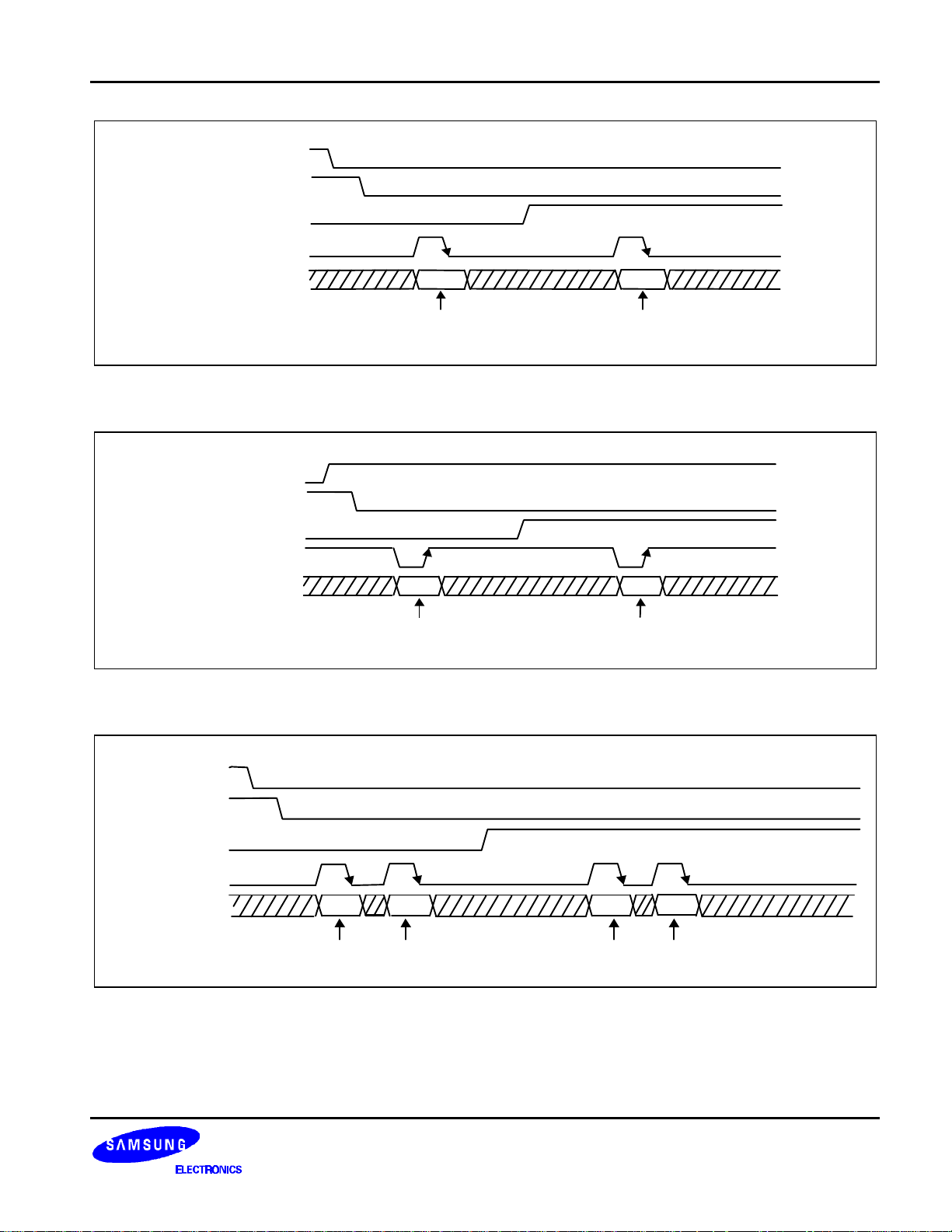
Figure 3. Timing Diagram of 8-bit Parallel Bus Mode Data Transfer (68-series MPU Mode)
RES
CSB
RS
E
to DB7
Instruction
Data
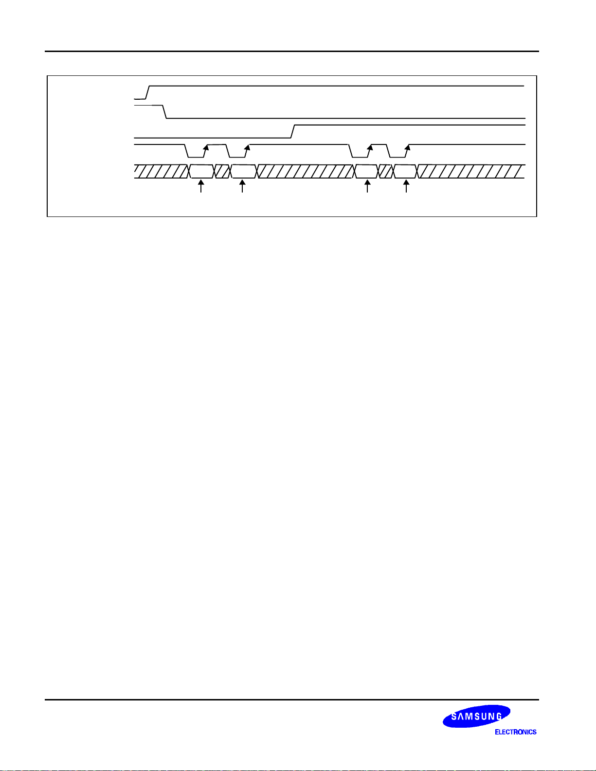
Figure 4. Timing Diagram of 8-bit Parallel Bus Mode Data Transfer (80-series MPU Mode)
upper
lower
upper
lower
Instruction Write Data Write
Figure 5. Timing Diagram of 4-bit Parallel Bus Mode Data Transfer (68-series MPU Mode)
11
S6A0090 64 SEG / 26 COM DRIVER & CONTROLLER FOR STN LCD
RES
CSB
RS
E
DB0 to DB7
4-bit
4-bit
4-bit
4-bit
upper
lower
upper
lower
Instruction Write Data Write
Figure 6. Timing Diagram of 4-bit Parallel Bus Mode Data Transfer (80-series MPU Mode)
12
64 SEG / 26 COM DRIVER & CONTROLLER FOR STN LCD S6A0090
D7D6D5D4D3D2D1D0D7
123456789
Interface with MPU in Serial Mode (PS = "Low")
When PS input pin is "Low", clock synchronized serial interface mode is selected. At this time, five ports, SCL
(DB6, synchronizing transfer clock), SI (DB7, serial input data), RS (register selection input) and CSB (chip
selection input) are used. By setting CSB to "Low", S6A0090 can receive SCL input. If CSB is set to "High",
S6A0090 resets the internal 8-bit shift register and 3-bit counter. Serial data is input in the order of "D7, D6, D5,
D4, D3, D2, D1, D0" from the serial data input pin (SI = DB7) at the rising edge of serial clock (SCL = DB6). At the
rising edge of the 8th serial clock, the serial data (D7–D0) is converted into 8-bit bus mode data. The RS input of
the DR / IR selection is latched at the rising edge of the 8th serial clock (SCL).
CSB
SI (DB7)
SCL (DB6)
RS
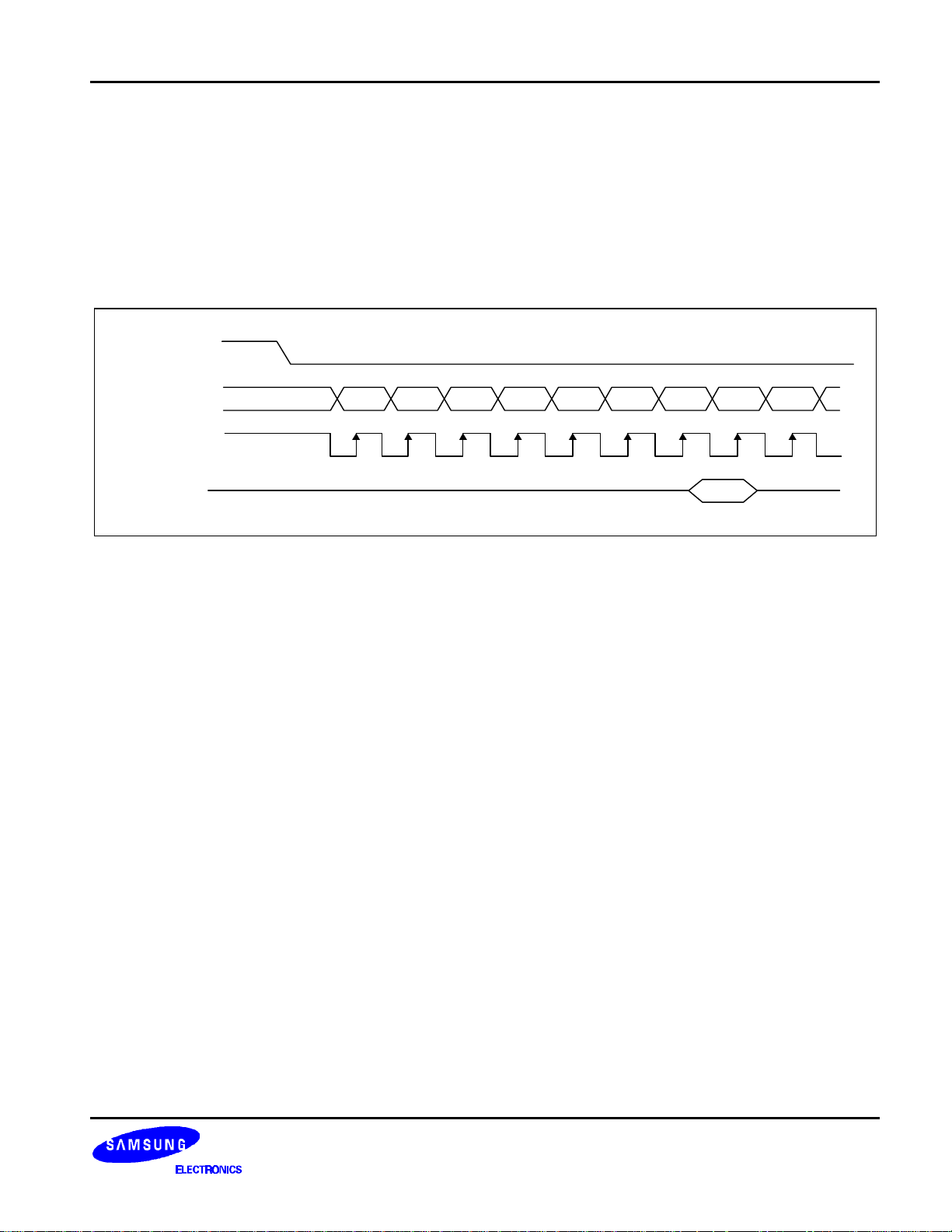
Figure 7. Timing Diagram of Serial Data Transfer
13
 Loading...