

Samsung S6A0075 Datasheet
100 SEG / 34 COM DRIVER & CONTROLLER FOR DOT MATRIX LCD
S6A0075
written permission of LCD Driver IC Team.
June. 2000.
Ver. 0.0
Contents in this document are subject to change without notice. No part of this document may be reproduced
or transmitted in any form or by any means, electronic or mechanical, for any purpose, without the express

S6A0075 100 SEG / 34 COM DRIVER & CONTROLLER FOR DOT MATRIX LCD
INTRODUCTION
S6A0075 is a dot matrix LCD driver & controller LSI which is fabricated by low power CMOS technology. It can
display 1, 2, or 4 lines with 5 x 8 or 6 x 8 dots format.
FUNCTIONS
• Character type dot matrix LCD driver & controller
• Internal driver: 34 common and 100 segment signal output
• Easy interface with 4-bit or 8-bit MPU
• Clock synchronized serial interface
• 5 x 8 dot matrix / 6 x 8 dot matrix possible
• Bi-directional shift function
• All character reverse display
• Display shift per line
• Voltage converter for LCD drive voltage: 13V max. (2 times/3 times)
• Various instruction functions
• Automatic power on reset
FEATURES
• Internal memory
- Character Generator ROM (CGROM): 9,600 bits (240 characters x 5 x 8 dot)
- Character Generator RAM (CGRAM): 64 x 8 bits (8 characters x 5 x 8 dot)
- Segment Icon RAM (SEGRAM): 16 x 8 bits (96 icons max.)
- Display Data RAM (DDRAM): 80 x 8 bits (80 characters max.)
• Low power operation
- Power supply voltage range: 2.7 - 5.5V (VDD)
- LCD Drive voltage range: 3.0 - 13.0V (VDD - V5)
• CMOS process
• Programmable duty cycle: 1/17, 1/33
• Internal oscillator with an external resistor
• Bare chip available
2
100 SEG / 34 COM DRIVER & CONTROLLER FOR DOT MATRIX LCD S6A0075
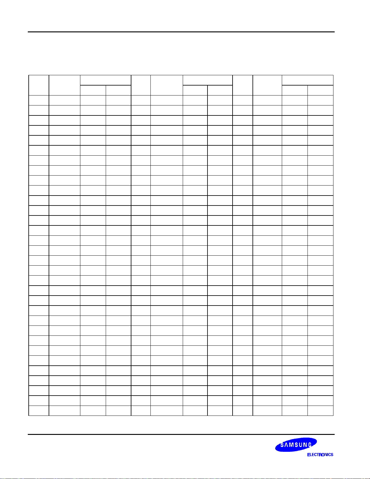
PROGRAMMABLE DUTY CYCLES
5-dot Font Width
Display Line
Numbers
1 1/17 1 line of 40 characters 80
2 1/33 2 lines of 40 characters 80
4 1/33 4 line of 20 characters 80
6-dot Font Width
Display Line
Numbers
1 1/17 1 line of 32 characters 96
2 1/33 2 lines of 32 characters 96
4 1/33 4 line of 16 characters 96
Duty Ratio
Single-chip Operation
Displayable Characters Possible Icons
Single-chip Operation
Duty Ratio
Displayable Characters Possible Icons
3
S6A0075 100 SEG / 34 COM DRIVER & CONTROLLER FOR DOT MATRIX LCD
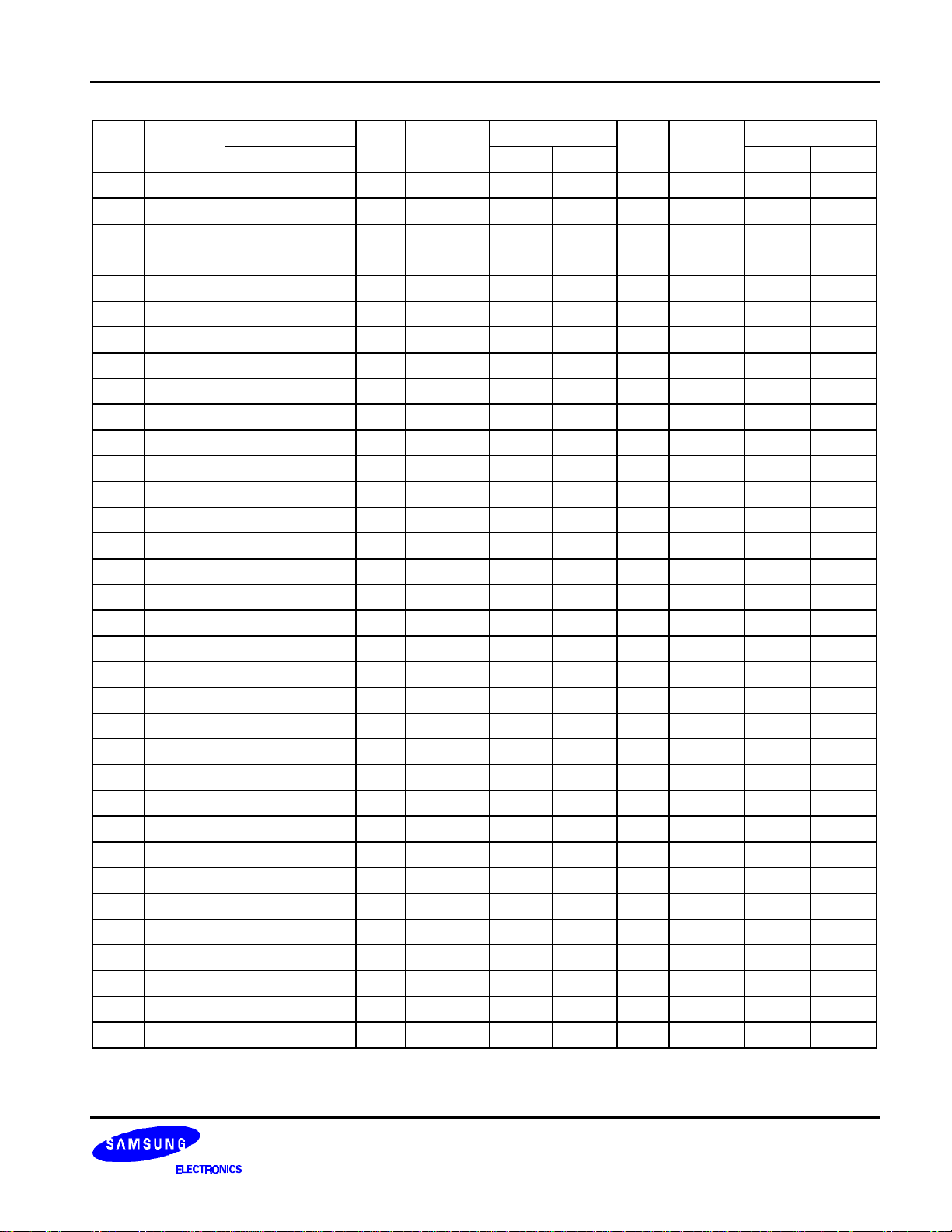
BLOCK DIAGRAM
OSC1 OSC2IE
RESET
RS/CS
E/SCLK
RW/SID
DB4-DB7
DB3-DB1
DB0-SOD
Vci
C1
C2
V5OUT2
V5OUT3
Power on Reset
(POR)
IM
Instruction
8
System
Interface
Serial
4-bit
8-bit
Input/
Output
Buffer
Voltage Converter
Register
(IR)
7
Data
8 8
Register
(DR)
8
Busy Flag
Segment
RAM
(SEGRAM)
16 bytes
Oscillator
Instruction
Decoder
Address
Counter
7
3 7 8
Character
Generator
RAM
(CGRAM)
64 bytes
5/6
Parallel/Serial Converter and
Smooth Scroll Circuit
Timing Generator
7
Display Data
RAM (DDRAM)
96 x 8-bit
8
8
Character
Generator
ROM
(CGROM)
9600 bits
5
100-bit
Register
Cursor and
Blink
Controller
Shift
34-bit
Shift
Register
100-bit
Latch
Circuit
Driver
Segment
Driver
V1 - V5
COM0COM33
COM1COM100
Common
LCD Driver
Voltage Selector
VDD
GND(VSS)
4
100 SEG / 34 COM DRIVER & CONTROLLER FOR DOT MATRIX LCD S6A0075
DB0/SOD
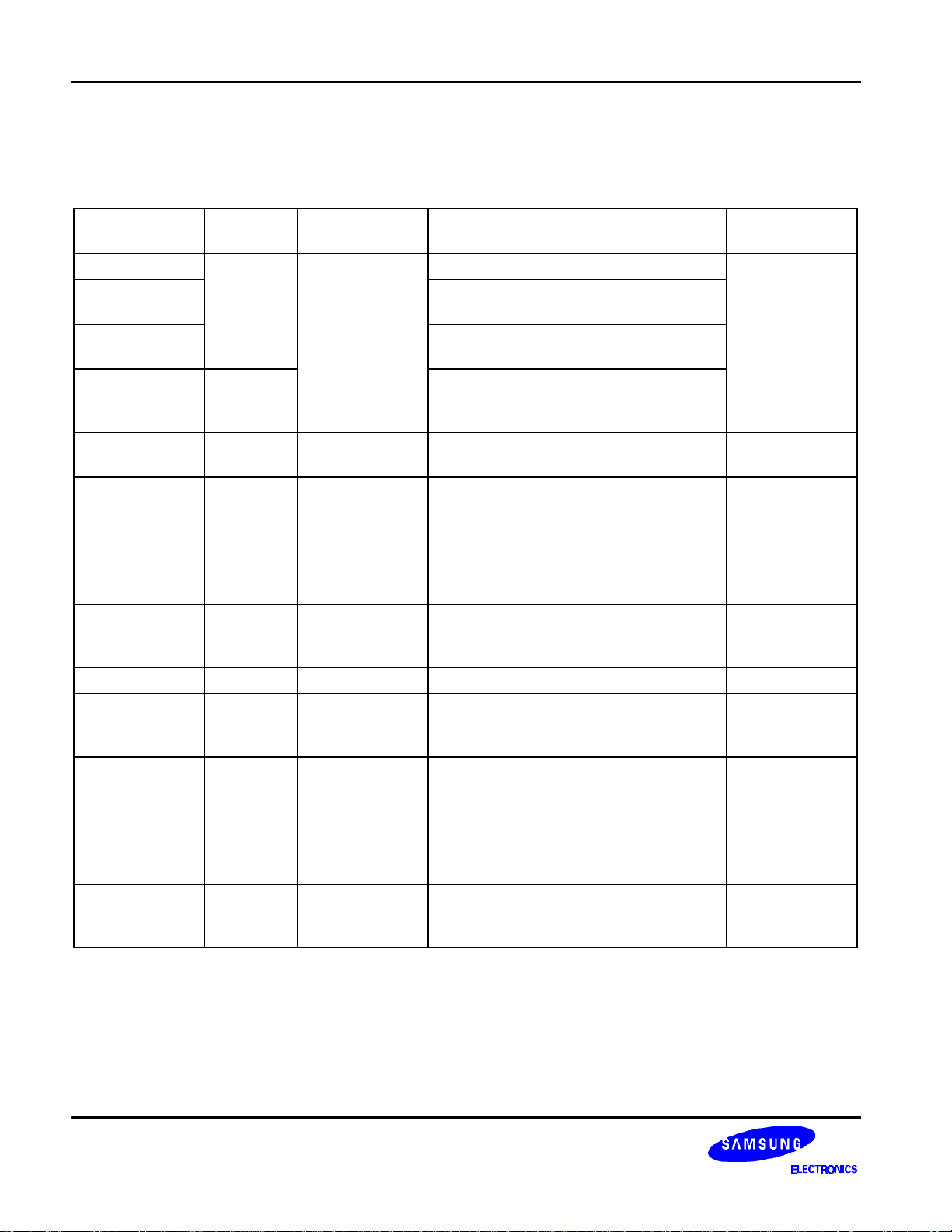
PAD CONFIGURATION
SEG67
SEG66
SEG65
SEG64
SEG63
SEG62
SEG61
SEG60
SEG59
SEG58
SEG57
SEG56
SEG55
SEG54
SEG53
SEG52
SEG51
SEG50
SEG49
SEG48
SEG47
SEG46
SEG45
SEG44
SEG43
SEG42
SEG41
SEG40
SEG39
SEG38
SEG37
SEG36
SEG35
SEG34
163
162
161
160
159
158
157
156
155
154
153
152
151
150
149
148
147
146
145
144
143
142
141
140
139
138
137
136
135
134
133
132
131
130
SEG68
SEG69
SEG70
SEG71
SEG72
SEG73
SEG74
SEG75
SEG76
SEG77
SEG78
SEG79
SEG80
SEG81
SEG82
SEG83
SEG84
SEG85
SEG86
SEG87
SEG88
SEG89
SEG90
SEG91
SEG92
SEG93
SEG94
SEG95
SEG96
SEG97
SEG98
SEG99
SEG100
COM9
COM10
COM11
COM12
COM13
COM14
COM15
COM16
COM25
COM26
COM27
COM28
COM29
COM30
COM31
COM32
COM33
10
11
12
13
14
15
16
17
18
19
20
21
22
23
24
25
26
27
28
29
30
31
32
33
34
35
36
37
38
39
40
41
42
43
44
45
46
47
48
49
50
1
2
3
4
5
6
7
8
9
(0, 0) Y
X
Chip size: 7450 x 5340
PAD size: 100
Unit: µm
S6A0075
×
100
129
128
127
126
125
124
123
122
121
120
119
118
117
116
115
114
113
112
111
110
109
108
107
106
105
104
103
102
101
100
99
98
97
96
95
94
93
92
91
90
89
88
87
86
85
84
83
82
81
80
SEG33
SEG32
SEG31
SEG30
SEG29
SEG28
SEG27
SEG26
SEG25
SEG24
SEG23
SEG22
SEG21
SEG20
SEG19
SEG18
SEG17
SEG16
SEG15
SEG14
SEG13
SEG12
SEG11
SEG10
SEG9
SEG8
SEG7
SEG6
SEG5
SEG4
SEG3
SEG2
SEG1
COM0
COM1
COM2
COM3
COM4
COM5
COM6
COM7
COM8
COM17
COM18
COM19
COM20
COM21
COM22
COM23
COM24
5152535455565758596061626364656667686970717273747576777879
IE
OSC2
OSC1
IM
RESET
VSS1
RS/CS
RW/SID
DB1
E/SCLK
DB2
DB3
DB4
DB5
DB6
DB7
VCI
C2
C1
VSS2
V5OUT2
V5V4V3V2V1
V5OUT3
DD
V
5
S6A0075 100 SEG / 34 COM DRIVER & CONTROLLER FOR DOT MATRIX LCD
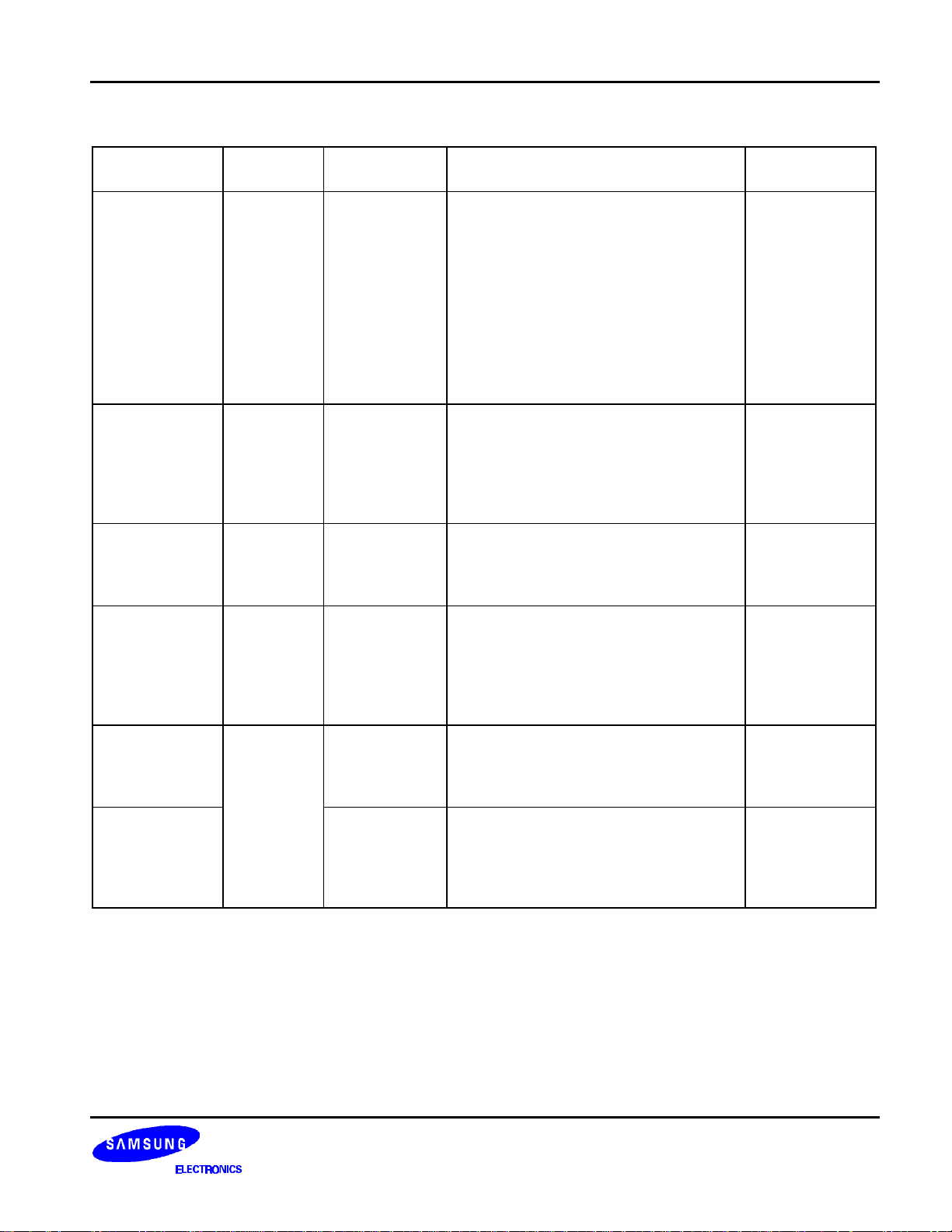
PAD CENTER COORDINATES
Table 1. Pad Location
Pad
No.
1 SEG68 -2975 -2504 33 SEG100 1024 -2504 65 DB4 3559 0
2 SEG69 -2850 -2504 34 COM9 1262 -2504 66 DB5 3559 125
3 SEG70 -2725 -2504 35 COM10 1387 -2504 67 DB6 3559 250
4 SEG71 -2600 -2504 36 COM11 1512 -2504 68 DB7 3559 375
5 SEG72 -2475 -2504 37 COM12 1637 -2504 69 VCI 3559 500
6 SEG73 -2350 -2504 38 COM13 1762 -2504 70 C2 3559 625
7 SEG74 -2225 -2504 39 COM14 1887 -2504 71 C1 3559 750
8 SEG75 -2100 -2504 40 COM15 2012 -2504 72 VSS2 3559 875
9 SEG76 -1975 -2504 41 COM16 2137 -2504 73 V5OUT2 3559 1000
10 SEG77 -1850 -2504 42 COM25 2262 -2504 74 V5OUT3 3559 1125
11 SEG78 -1725 -2504 43 COM26 2387 -2504 75 V5 3559 1250
12 SEG79 -1600 -2504 44 COM27 2512 -2504 76 V4 3559 1375
13 SEG80 -1475 -2504 45 COM28 2637 -2504 77 V3 3559 1500
14 SEG81 -1350 -2504 46 COM29 2762 -2504 78 V2 3559 1625
15 SEG82 -1225 -2504 47 COM30 2887 -2504 79 V1 3559 1750
16 SEG83 -1100 -2504 48 COM31 3012 -2504 80 COM24 3262 2504
17 SEG84 -975 -2504 49 COM32 3137 -2504 81 COM23 3137 2504
18 SEG85 -850 -2504 50 COM33 3262 -2504 82 COM22 3012 2504
19 SEG86 -725 -2504 51 VDD 3559 -1750 83 COM21 2887 2504
20 SEG87 -600 -2504 52 OSCC 3559 -1625 84 COM20 2762 2504
21 SEG88 -475 -2504 53 OSC1 3559 -1500 85 COM19 2637 2504
22 SEG89 -350 -2504 54 RESET 3559 -1375 86 COM18 2512 2504
23 SEG90 -225 -2504 55 IM 3559 -1250 87 COM17 2387 2504
24 SEG91 -100 -2504 56 IE 3559 -1125 88 COM8 2262 2504
25 SEG92 24 -2504 57 VSS1 3559 -1000 89 COM7 2137 2504
26 SEG93 149 -2504 58 RS/CS 3559 -875 90 COM6 2012 2504
27 SEG94 274 -2504 59 RW/SID 3559 -750 91 COM5 1887 2504
28 SEG95 399 -2504 60 E/SCLK 3559 -625 92 COM4 1762 2504
29 SEG96 524 -2504 61 DB0/SOD 3559 -500 93 COM3 1637 2504
30 SEG97 649 -2504 62 DB1 3559 -375 94 COM2 1512 2504
31 SEG98 774 -2504 63 DB2 3559 -250 95 COM1 1387 2504
32 SEG99 899 -2504 64 DB3 3559 -125 96 COM0 1262 2504
Pad
Name
Coordinate Coordinate Coordinate
X Y
Pad
No.
Pad
Name
X Y
Pad
No.
Pad
Name
X Y
Table 1. Pad Location (Continued)
6
100 SEG / 34 COM DRIVER & CONTROLLER FOR DOT MATRIX LCD S6A0075
Pad
No.
Pad
Name
Coordinate Coordinate Coordinate
X Y
Pad
No.
Pad
Name
X Y
97 SEG1 1024 2504 131 SEG35 -3559 1937
98 SEG2 899 2504 132 SEG36 -3559 1812
99 SEG3 774 2504 133 SEG37 -3559 1687
100 SEG4 649 2504 134 SEG38 -3559 1562
101 SEG5 524 2504 135 SEG39 -3559 1437
102 SEG6 399 2504 136 SEG40 -3559 1312
103 SEG7 274 2504 137 SEG41 -3559 1187
104 SEG8 149 2504 138 SEG42 -3559 1062
105 SEG9 24 2504 139 SEG43 -3559 937
106 SEG10 -100 2504 140 SEG44 -3559 812
107 SEG11 -225 2504 141 SEG45 -3559 687
108 SEG12 -350 2504 142 SEG46 -3559 562
109 SEG13 -475 2504 143 SEG47 -3559 437
110 SEG14 -600 2504 144 SEG48 -3559 312
111 SEG15 -725 2504 145 SEG49 -3559 187
112 SEG16 -850 2504 146 SEG50 -3559 62
113 SEG17 -975 2504 147 SEG51 -3559 -62
114 SEG18 -1100 2504 148 SEG52 -3559 -187
115 SEG19 -1225 2504 149 SEG53 -3559 -312
116 SEG20 -1350 2504 150 SEG54 -3559 -437
117 SEG21 -1475 2504 151 SEG55 -3559 -562
118 SEG22 -1600 2504 152 SEG56 -3559 -687
119 SEG23 -1725 2504 153 SEG57 -3559 -812
120 SEG24 -1850 2504 154 SEG58 -3559 -937
121 SEG25 -1975 2504 155 SEG59 -3559 -1062
122 SEG26 -2100 2504 156 SEG60 -3559 -1187
123 SEG27 -2225 2504 157 SEG61 -3559 -1312
124 SEG28 -2350 2504 158 SEG62 -3559 -1437
125 SEG29 -2475 2504 159 SEG63 -3559 -1562
126 SEG30 -2600 2504 160 SEG64 -3559 -1687
127 SEG31 -2725 2504 161 SEG65 -3559 -1812
128 SEG32 -2850 2504 162 SEG66 -3559 -1937
129 SEG33 -2975 2504 163 SEG67 -3559 -2062
130 SEG34 -3559 2062
Pad
No.
Pad
Name
X Y
7
S6A0075 100 SEG / 34 COM DRIVER & CONTROLLER FOR DOT MATRIX LCD
PAD DESCRIPTION
Table 2. Pad Description
Pad (No)
Input/
Output
Name Description Interface
VDD (51) for logical circuit (+3V, +5V)
VSS1, VSS2
(57,72)
V1 - V5
(79 - 75)
-
Power supply
0V (GND)
Power supply
Bias voltage level for LCD driving.
Input voltage to the voltage converter to
Vci (69) Input
generate LCD drive voltage
(Vci = 2.5 - 4.5V).
SEG1 - SEG100
(97- 33)
COM0 - COM33
(80 - 96, 34 - 50)
OSC1, OSC2
(53, 52)
C1, C2
(71, 70)
Output Segment output Segment signal output for LCD drive. LCD
Output Common output Common signal output for LCD drive. LCD
Input
(OSC1),
Output
(OSC2)
Input
Oscillator
External
capacitance
input
When use internal oscillator, connect
external Rf resistor.
If external clock is used, connect it to
OSC1.
To use the voltage converter (2 times /3
times), these pins must be connected to
the external capacitance.
External
resistor/oscillator
(OSC1)
External
capacitance
RESET (54) Input Reset pin Initialized to low -
When IE = "High", Instruction set is
selected as Table 6. When IE = "Low",
Instruction set is selected as Table 10.
IE (56) Input
Select pin of
instruction set
The value of Vci is converted two times.
V5OUT2 (73)
Output
V5OUT3 (74)
IM (55) Input
Two times
converter output
Three times
converter output
Interface mode
selection
To use three times converter, the same
capacitance as that of C1-C2 should be
connected here.
The value of Vci is converted three
times.
Select Interface mode with the MPU.
When IM = "Low": Serial mode,
When IM = "High": 4-bit/8-bit bus mode.
V5 capacitance
-
V5
-
8
100 SEG / 34 COM DRIVER & CONTROLLER FOR DOT MATRIX LCD S6A0075
Table 2. Pad Description (Continued)
Pad (No)
Input/
Output
RS/CS (58) Input
RW/SID (59) Input
E/SCLK (60) Input
DB0/SOD (61)
Input.Output/
Output
DB1 - DB3
(62 - 64)
Input.Output
DB4 - DB7
(65 - 68)
Name Description Interface
When bus mode, used as register
selection input.
When RS/CS = "High", data register is
selected.
Register select/
chip select
When RS/CS = "Low", instruction
register is selected.
When serial mode, used as chip
selection input.
When RS/CS = "Low", selected.
When RS/CS = "High", not elected.
(low access enable)
When bus mode, used as read/write
Read/Write/
Serial input
data
selection input.
When RW/SID = "High", read operation.
When RW/SID = "Low", write operation.
When serial mode, used for data input
pin.
Read/Write
Enable/Serial
clock
When bus mode, used as read/write
enable signal.
When serial mode, used as serial clock
input pin.
When 8-bit bus mode, used as lowest biData bus 0
bit/serial output
data
directional data bit. During 4-bit bus
mode, open this pin.
When serial mode, used as serial data
output pin. If not in read operation, open
this pin.
When 8-bit bus mode, used as low order
Data bus 1-7
bi-directional data bus.
During 4-bit bus mode or serial mode,
open these pins.
When 8-bit bus mode, used as high
order bi-directional data bus. In case of
4-bit bus mode, used as both high and
low order. DB7 used for busy flag output.
During serial mode, open these pins.
MPU
MPU
MPU
MPU
MPU
MPU
9
S6A0075 100 SEG / 34 COM DRIVER & CONTROLLER FOR DOT MATRIX LCD
FUNCTION DESCRIPTION
SYSTEM INTERFACE
This chip has all three kinds interface type with MPU: serial, 4-bit bus and 8-bit bus. Serial and bus (4-bit/8-bit) is
selected by IM input, and 4-bit bus and 8-bit bus is selected by DL bit in the instruction register. During read or
write operation, two 8-bit registers are used. one is data register (DR), the other is instruction register (IR). The
data register (DR) is used as temporary data storage place for being written into or read from
DDRAM/CGRAM/SEGRAM, target RAM is selected by RAM address setting instruction. Each internal operation,
reading from or writing into RAM, is done automatically. So to speak, after MPU reads DR data, the data in the
next DDRAM/CGRAM/SEGRAM address is transferred into DR automatically. Also after MPU writes data to DR,
the data in DR is transferred into DDRAM/CGRAM/SEGRAM automatically. The Instruction register (IR) is used
only to store instruction code transferred from MPU. MPU cannot use it to read instruction data. To select
register, use RS/CS input pin in 4-bit/8-bit bus mode (IM = "High") or RS bit in serial mode (IM = "Low").
RS R/W Operation
0 0 Instruction write operation (MPU writes Instruction code into IR)
0 1 Read busy flag (DB7) and address counter (DB0 - DB6)
1 0 Data write operation (MPU writes data into DR)
1 1 Data read operation (MPU reads data from DR)
10
100 SEG / 34 COM DRIVER & CONTROLLER FOR DOT MATRIX LCD S6A0075
BUSY FLAG (BF)
When BF = "High", it indicates that the internal operation is being processed. So during this time the next
instruction cannot be accepted. BF can be read, when RS = Low and R/W = High (Read Instruction Operation),
through DB7. Before executing the next instruction, be sure that BF is not high.
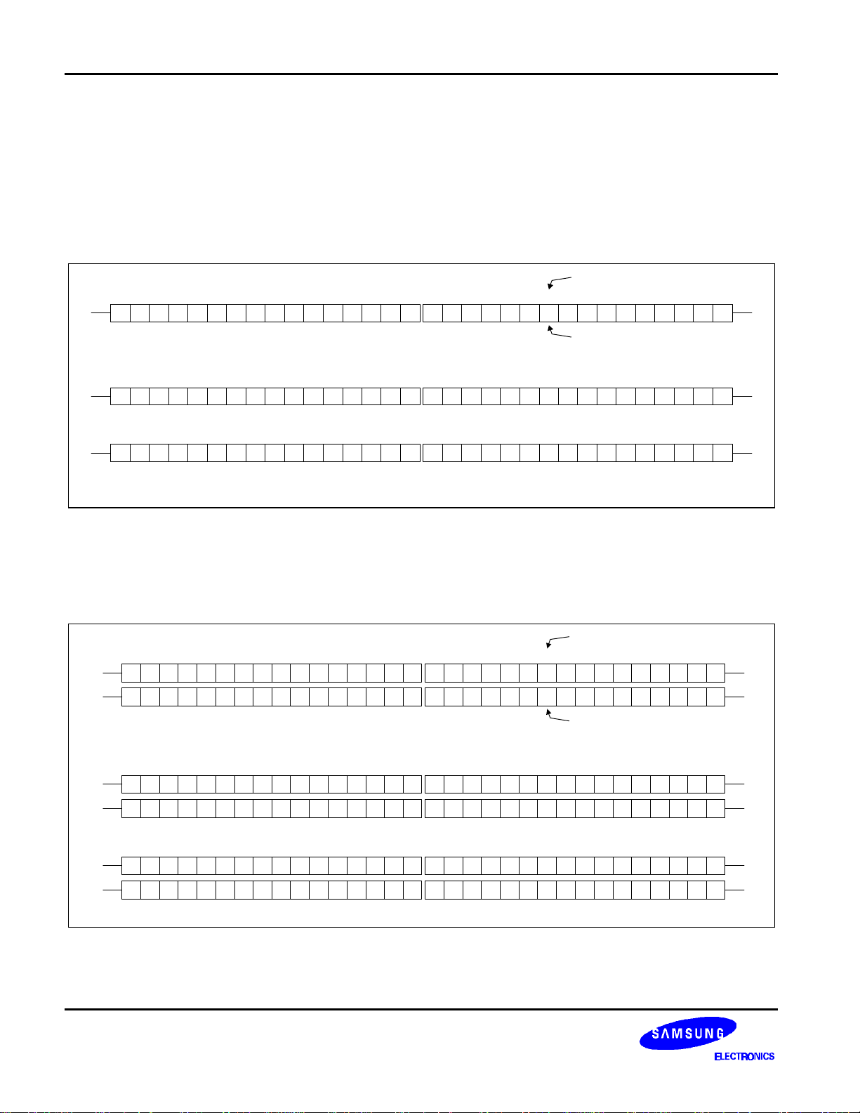
DISPLAY DATA RAM (DDRAM)
DDRAM stores display data of maximum 80 x 8 bits (80 characters). DDRAM address is set in the address
counter (AC) as a hexadecimal number. (refer to Figure 1.)
MSB LSB
AC6 AC5 AC4 AC3 AC2 AC1 AC0
Figure 1. DDRAM Address
Display of 5-Dot Font Width Character
5-dot 1-line Display
In case of 1-line display with 5-dot font, the address range of DDRAM is 00H-4FH. (refer to Figure 2)
COM1
COM8
COM1
COM8
COM1
COM8
1 2 3 4 5
00 01 02 03 04
SEG1
1 2 3 4 5
01 02 03 04
1 2 3 4 5
4F 00
01 02 03 04
6 7 8 9 10
05 06 07 08 09 0A 0E 0F
S6A0075
21 22 23 24
14 15 16 17
SEG1
6 7 8 9 10
05 06 07 08 09 0A 0E 1F
21 22 23 24
15 16 17
6 7 8 9 101211 12 13 14 15
05 06 07 08 09 0A 0E 1F
11 12 13 14 15
0B 0C 0D 10 11
25 26 27 28 29
18 19 1A 1B 1C
11 12 13 14 15
0B 0C 0D 10 11
25 26 27 28 29
18 19 1A 1B 1C
(After Shift Left)
0B 0C 0D 10 11
16 17 18 19 20
12 13
SEG100
Display Position
30 31 32 33 34 35
21 221F 201E1D
DDRAM Address
S6A0075
16 17 18 19 20
12 13
30 31 32 33 34 35
16 17 18 19 20
14
21 221F 201E1D
23 24 25 26 27
36 37 38 39 40
23 24 25 26 27
SEG100
36 37 38 39 40
28
COM9
COM16
COM9
COM16
21 22 23 24
13 14
15 16 17
Figure 2. 1-line x 40ch. Display
25 26 27 28 29
18 19 1A 1B 1C
(After Shift Right)
30 31 32 33 34 35
21 221F 201E1D
36 37 38 39 40
23 24 25 26
COM9
COM16
11
S6A0075 100 SEG / 34 COM DRIVER & CONTROLLER FOR DOT MATRIX LCD
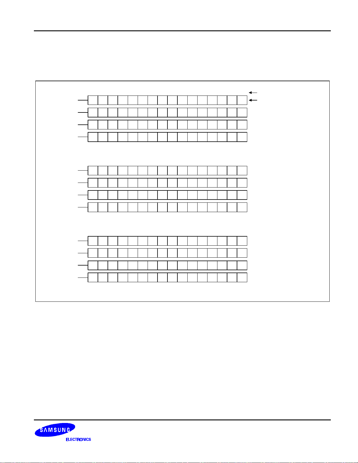
5-dot 2-line Display
In case of 2-line display with 5-dot font, the address range of DDRAM is 00H-27H, 40H-67H (refer to Figure 3).
COM1
COM8
COM17
COM24
COM1
COM8
COM17
COM24
1 2 3 4 5
00 01 02 03 04
40 41 42 43 44
SEG1
1 2 3 4 5
01 02 03 04
41 42 43 44
6 7 8 9 10
05 06 07 08 09 0A 0E 0F
45 46 47 48 49 4A 4E 4F
S6A0075
21 22 23 24
14 15 16 17
54 55 56 57 58 59 5A 5B 5C 63 64 65 66 67
SEG1
6 7 8 9 10
05 06 07 08 09 0A 0E 0F
21 22 23 24
15 16 17
55 56 57 58 59 5A 5B 5C 63 64 65 66 67
11 12 13 14 15
0B 0C 0D 10 11
4B 4C 4D 50 51 52 53
25 26 27 28 29
18 19 1A 1B 1C
11 12 13 14 15
0B 0C 0D 10 11
4B 4C 4D 50 51 52 5345 46 47 48 49 4A 4E 4F 54
25 26 27 28 29
18 19 1A 1B 1C
(After Shift Left)
16 17 18 19 20
30 31 32 33 34 35
16 17 18 19 20
30 31 32 33 34 35
12 13
SEG100
Display Position
36 37 38 39 40
21 221F 201E1D
61 625F 605E5D
DDRAM Address
S6A0075
12 13
21 221F 201E1D
61 625F 605E5D 40
23 24 25 26 27
14
36 37 38 39 40
23 24 25 26 27
SEG100
00
COM9
COM16
COM25
COM32
COM9
COM16
COM25
COM32
COM1
COM8
COM17
COM24
1 2 3 4 5
01 02 03 04
00
27
41 42 43 44
6 7 8 9 101211 12 13 14 15
05 06 07 08 09 0A 0E 0F
21 22 23 24
13 14
15 16 17
55 56 57 58 59 5A 5B 5C 63 64 65 66
25 26 27 28 29
0B 0C 0D 10 11
4B 4C 4D 50 51 5245 46 47 48 49 4A 4E 4F67 40
18 19 1A 1B 1C
(After Shift Right)
16 17 18 19 20
30 31 32 33 34 35
Figure 3. 2-line x 40ch. Display (5-dot Font Width)
36 37 38 39 40
21 221F 201E1D
61 625F 605E5D53 54
23 24 25 26
COM9
COM16
COM25
COM32
12
100 SEG / 34 COM DRIVER & CONTROLLER FOR DOT MATRIX LCD S6A0075
5-dot 4-line Display
In case of 4-line display with 5-dot font, the address range of DDARM is 00H-13H, 20H-33H, 40H -53H, 60H-73H
(refer to Figure 4).
COM1
COM8
COM9
COM16
COM17
COM24
COM25
COM32
COM1
COM8
COM9
COM16
COM17
COM24
COM25
COM32
COM1
COM8
COM9
COM16
COM17
COM24
COM25
COM32
1 2 3 4 5
00 01 02 03 04
21 22 23 24 25 26 27 28 2F 30 31 322D 2E2B 2C2A29 3320
40 41 42 43 44
61 62 63 64 65 66 67 68 6F 70 71 726D 6E6B 6C6A6960 73
SEG1
1 2 3 4 5
01 02 03 04
21 22 23 24 25 26 27 28 2F 30 31 322D 2E2B 2C2A29 33 20
41 42 43 44
61 62 63 64 65 66 67 68 6F 70 71 72 73
1 2 3 4 5
01 02 03 04
00
13
33 20
21 22 23 24 25 26 27 28 2F 30 31 32
41 42 43 44
61 62 63 64 65 66 67 68 6F 70 71 72
6 7 8 9 10
05 06 07 08 09 0A 0E 0F
6 7 8 9 10
05 06 07 08 09 0A 0E 0F
(After Shift Left)
6 7 8 9 101211 12 13 14 15
05 06 07 08 09 0A 0E 0F
(After Shift Right)
11 12 13 14 15
0B 0C 0D 10 11
4B 4C 4D 50 51 52 5345 46 47 48 49 4A 4E 4F
S6A0075
11 12 13 14 15
0B 0C 0D 10 11
4B 4C 4D 50 51 52 5345 46 47 48 49 4A 4E 4F 40
6D 6E6B 6C6A69 60
0B 0C 0D 10 11
2D 2E2B 2C2A29
4B 4C 4D 50 51 5245 46 47 48 49 4A 4E 4F53 40
6D 6E6B 6C6A6973 60
16 17 18 19 20
12 13
SEG100
16 17 18 19 20
12 13
16 17 18 19 20
Display Position
DDRAM Address
00
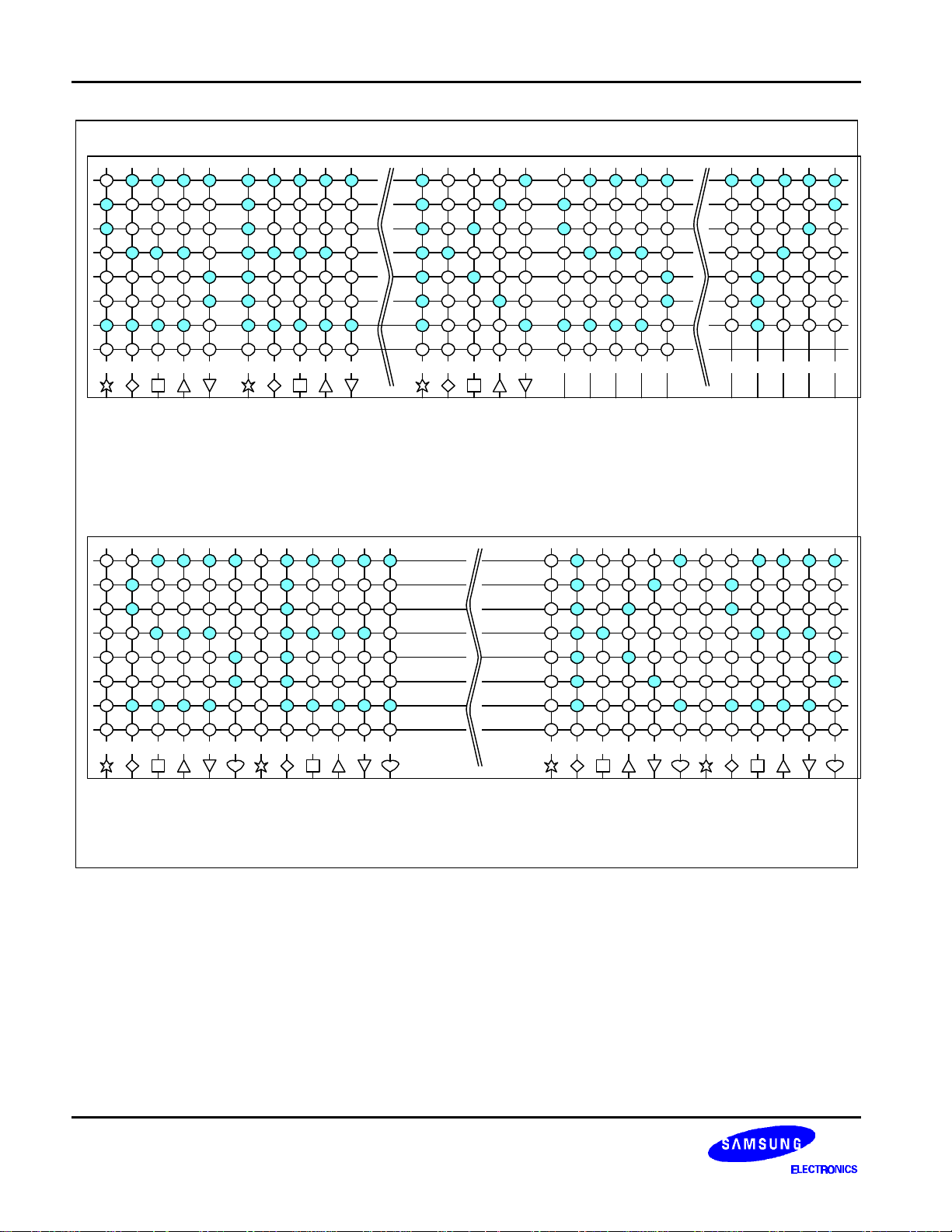
Figure 4. 4-line x 20ch. Display (5-dot Font Width)
13
S6A0075 100 SEG / 34 COM DRIVER & CONTROLLER FOR DOT MATRIX LCD
COM16
COM16
COM16
DISPLAY OF 6-DOT FONT WIDTH CHARACTER
When this device is used in 6-dot font width mode, SEG97, SEG98, SEG99 and SEG100 must be open.
6-dot 1-line Display
In case of 1-line display with 6-dot font, the address range of DDRAM is 00H-4FH (refer to Figure 5).
Display Position
COM1
COM8
1 2 3 4 5
00 01 02 03 04
SEG1
6 7 8 9 10 11 12 13 14 15
05 06 07 08 09 0A 0E 0F1610 11 12
S6A0075
0B 0C 0D
17 18 19 20
SEG96SEG1
21 22 23 24
13 14 15 16
25 26
17 18
19 1A 1B 1C
DDRAM Address
S6A0075
27 28 29 30
1D 1E
31 32
SEG96
COM9
1F
COM1
COM8
COM1
COM8
1 2 3 4 5
01 02 03 04
1 2 3 4 5
01 02 03 04
4F 00 0F 10
6 7 8 9 10 11 12 13 14 15
05 06 07 08 09 0A 0E 0F
6 7 8 9 10 11 12 13 14 15
05 06 07 08 09 0A 0E
0B 0C 0D
(After Shift Left)
0B 0C 0D
(After Shift Right)
16
17 18 19 20
11 12
10 20
16
17 18 19 20
21 22 23 24
13 14 15 16
21 22 23 24
11 12
13 14 15 16
17 18
25 26
27 28 29 30
19 1A 1B 1C
25 26
27 28 29 30
17 18
19 1A 1B 1C
1D 1E
31 32
1F
31 32
1D 1E
COM9
COM9
Figure 5. 1-line ×× 32ch. Display
6-dot 2-line Display
In case of 2-line display with 6-dot font, the address range of DDRAM is 00H-27H, 40H-67H (refer to Figure 6).
Display Position
COM1
COM8
COM17
COM24
COM1
COM8
COM17
COM24
COM1
COM8
COM17
COM24
1 2 3 4 5
00 01 02 03 04
40 41 42 43 44
SEG1
1 2 3 4 5
01 02 03 04
41 42 43 44 4B 4C 4D45 46 47 48 49 4A 4E 4F 51 52 53 54 55 56 57 58 59 5A 5B 5C 5D 5E 5F50 60
1 2 3 4 5
01 02 03 04
27 00 0F 10
41 42 43 44 4B 4C 4D45 46 47 48 49 4A 4E 51 52 53 54 55 56 57 58 59 5A 5B 5C 5D 5E67 40 4F 50
6 7 8 9 10 11 12 13 14 15
05 06 07 08 09 0A 0E 0F1610 11 12
S6A0075
6 7 8 9 10 11 12 13 14 15
05 06 07 08 09 0A 0E 0F
6 7 8 9 10 11 12 13 14 15
05 06 07 08 09 0A 0E
0B 0C 0D
4B 4C 4D45 46 47 48 49 4A 4E 4F 50 51 52 53 54 55 56 57 58 59 5A 5B 5C 5D 5E 5F
SEG96 SEG1
16
0B 0C 0D
0B 0C 0D
10 20
(After Shift Left)
16
(After Shift Right)
17 18 19 20
13 14 15 16
17 18 19 20
11 12
13 14 15 16
17 18 19 20
11 12
21 22 23 24
21 22 23 24
17 18
21 22 23 24
13 14 15 16
25 26
17 18
19 1A 1B 1C
DDRAM Address
S6A0075
25 26
19 1A 1B 1C
25 26
17 18
27 28 29 30
1D 1E
27 28 29 30
1D 1E
27 28 29 30
19 1A 1B 1C
31 32
1F
SEG96
31 32
1F
31 32
1D 1E
COM9
COM16
COM25
COM32
COM9
COM16
COM25
COM32
COM9
COM16
COM25
COM32
Figure 6. 2-line ×× 32ch. Display (6-dot font width)
14
100 SEG / 34 COM DRIVER & CONTROLLER FOR DOT MATRIX LCD S6A0075
6-dot 4-line Display
In case of 4-line display with 6-dot font, the address range of DDARM is 00H-13H, 20H-33H, 40H-53H, 60H-73H
(refer to Figure 7).
COM1
COM8
COM9
COM16
COM17
COM24
COM25
COM32
COM1
COM8
COM9
COM16
COM17
COM24
COM25
COM32
COM1
COM8
COM9
COM16
COM17
COM24
COM25
COM32
1 2 3 4 5
00 01 02 03 04
21 22 23 24 25 26 27 28 2F2D 2E2B 2C2A2920
40 41 42 43 44
61 62 63 64 65 66 67 68 6F6D 6E6B 6C6A6960
SEG1
1 2 3 4 5
01 02 03 04
21 22 23 24 25 26 27 28 2F 302D 2E2B 2C2A29
41 42 43 44
61 62 63 64 65 66 67 68 6F 70
1 2 3 4 5
01 02 03 04
00
13
33 20
21 22 23 24 25 26 27 28
41 42 43 44
61 62 63 64 65 66 67 68
6 7 8 9 10 11 12 13 14 15
05 06 07 08 09 0A 0E 0F
S6A0075
6 7 8 9 10 11 12 13 14 15
05 06 07 08 09 0A 0E 0F
(After Shift Left)
6 7 8 9 10 11 12 13 14 15
05 06 07 08 09 0A 0E
(After Shift Right)
0B 0C 0D
4B 4C 4D45 46 47 48 49 4A 4E 4F
SEG96
0B 0C 0D 10
4B 4C 4D 5045 46 47 48 49 4A 4E 4F
6D 6E6B 6C6A69
0B 0C 0D
2D 2E2B 2C2A29
4B 4C 4D45 46 47 48 49 4A 4E53 40
6D 6E6B 6C6A6973 60
16
16
16
Display Position
DDRAM Address
Figure 7. 4-line ×× 16ch. Display (6-dot Font Width)
15

S6A0075 100 SEG / 34 COM DRIVER & CONTROLLER FOR DOT MATRIX LCD
TIMING GENERATION CIRCUIT
Timing generation circuit generates clock signals for the internal operations.
ADDRESS COUNTER (AC)
Address Counter(AC) stores DDRAM/CGRAM/SEGRAM address, transferred from IR. After writing into (reading
from) DDRAM/CGRAM/SEGRAM, AC is automatically increased (decreased) by 1. When RS = "Low" and R/W =
"High", AC can be read through DB0-DB6
CURSOR/BLINK CONTROL CIRCUIT
It controls cursor/blink ON/OFF and black/white inversion at cursor position.
LCD DRIVER CIRCUIT
LCD Driver circuit has 34 common and 100 segment signals for LCD driving. Data from
SEGRAM/CGRAM/CGROM is transferred to 100-bit segment latch serially, and then it is stored to 100-bit shift
latch. When each com is selected by 34-bit common register, segment data also output through segment driver
from 100-bit segment latch. In case of 1-line display mode, COM0-COM17 have 1/17 duty, and in 2-line or 4-line
mode, COM0-COM33 have 1/33 duty ratio.
16
100 SEG / 34 COM DRIVER & CONTROLLER FOR DOT MATRIX LCD S6A0075
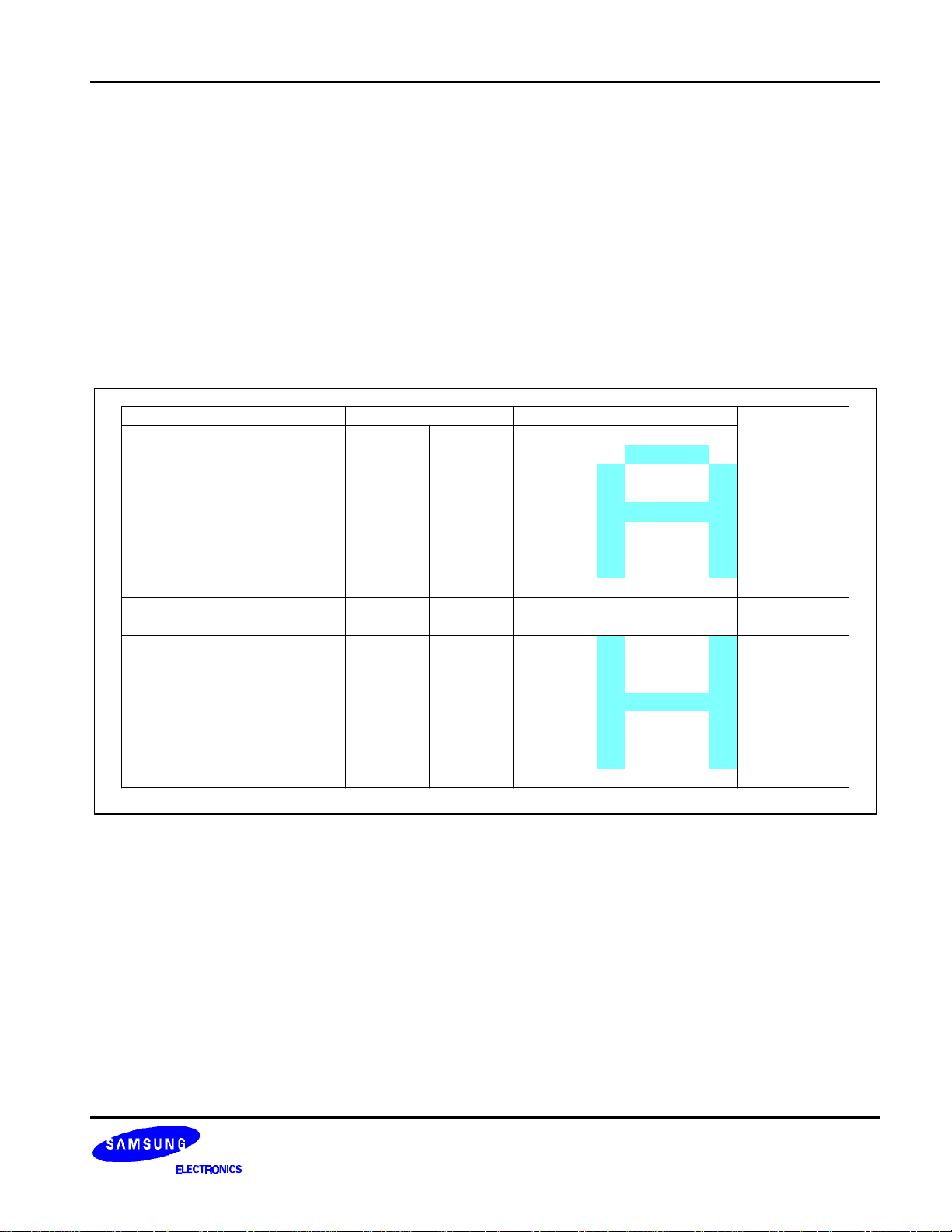
CGROM (CHARACTER GENERATOR ROM)
CGROM has 5 × 8 dots 240 Character Pattern.
CGRAM (CHARACTER GENERATOR RAM)
CGRAM has up to 5 × 8 dots 8 characters. By writing font data to CGRAM, user defined character can be used
(refer to Table 4).
5 ×× 8 dots Character Pattern
Table 4. Relationship between Character Code(DDRAM) and Character Pattern(CGRAM)
Character Code (DDRAM data) CGRAM Address CGRAM Data
D7 D6 D5 D4 D3 D2 D1 D0 A5 A4 A3 A2 A1 A0 P7 P6 P5 P4 P3 P2 P1 P0
0 0 x0 0 0 0 0 0 0 0 0 0
0 0
0 0
.
.
.
.
.
.
.
0 0 0 x0 1 1 1 1 1 1 0 0 0
.
.
.
.
.
.
.
.
.
.
.
.
.
.
.
.
.
1
0
1 1
0 0
1
0
1 1
1 1
1 1 1
.
.
0 0
0 0
1
0
1 1
0 0
1
0
1 1
1 1
1 1 1
B1 B0 x 0 0
1
.
.
.
.
0
1
0
.
B1 B0 x
.
.
.
.
.
1 1 10
1
0 0 0
1
0 0 0
1
1 1 1 1
1
0 0 0
1
0 0 0
1
0 0 0
0
0 0 0 0
.
.
01 10 0
1
0 0 0
1
0 0 0
1
1 1 1 1
1
0 0 0
1
0 0 0
1
0 0 0
0
0 0 0 0
Pattern
Number
Pattern 1
1
1
1
1
1
.
.
Pattern 8
1
1
1
1
1
17
S6A0075 100 SEG / 34 COM DRIVER & CONTROLLER FOR DOT MATRIX LCD
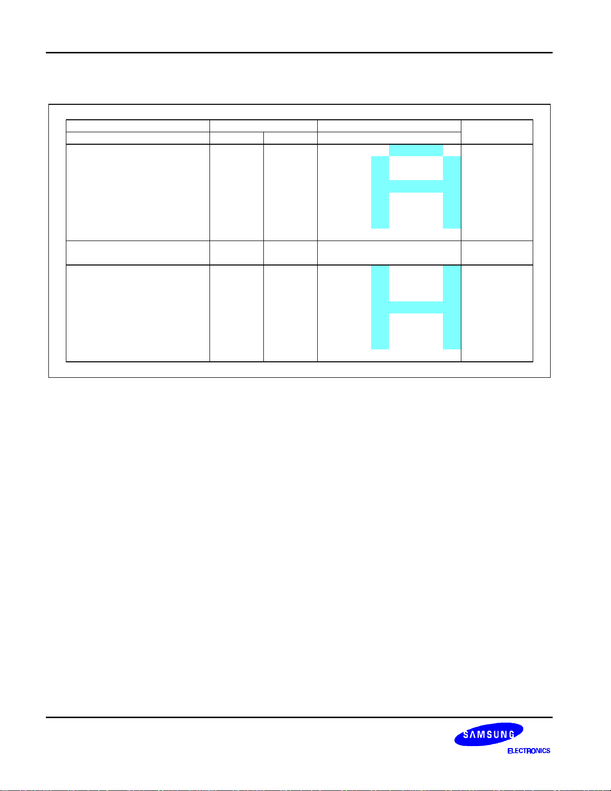
6 x 8 Dots Character Pattern
Character Code (DDRAM data) CGRAM Address CGRAM Data
D7 D6 D5 D4 D3 D2 D1 D0 A5 A4 A3 A2 A1 A0 P7 P6 P5 P4 P3 P2 P1 P0
0 0 x0 0 0 0 0 0 0 0 0 0
0 0
0 0
.
.
.
.
.
.
.
0 0 0 x0 1 1 1 1 1 1 0 0 0
.
.
.
.
.
.
.
.
.
.
.
.
.
.
.
.
.
1
0
1 1
0 0
1
0
1 1
1 1
1 1 1
.
.
0 0
0 0
1
0
1 1
0 0
1
0
1 1
1 1
1 1 1
B1 B0 0 0 0
1
0
B1 B0 0
1
0
0
0
.
0
.
.
0
.
0
.
0
0
0
0
.
0
.
.
0
.
0
.
0
0
1 1 10
1
0 0 0
1
0 0 0
1
1 1 1 1
1
0 0 0
1
0 0 0
1
0 0 0
0
0 0 0 0
.
.
01 10 0
1
0 0 0
1
0 0 0
1
1 1 1 1
1
0 0 0
1
0 0 0
1
0 0 0
0
0 0 0 0
1
1
1
1
1
1
1
1
1
1
Pattern
Number
Pattern 1
Pattern 8
1. When BE (Blink Enable bit) = "High", blink is controlled by B1 and B0 bit.
In case of 5-dot font width, when B1 = "1", enabled dots of P0-P4 will blink, and when B1 = "0" and B0 = "1", enabled
dots in P4 will blink, when B1 = "0" and B0 = "0", blink will not happen.
In case of 6-dot font width, when B1 = "1", enabled dots of P0-P5 will blink, and when B1 = "0" and B0 = "1", enabled
dots of P5 will blink, when B1 = "0" and B0 = "0", blink will not happen.
2 "X": Don't care
.
.
18
100 SEG / 34 COM DRIVER & CONTROLLER FOR DOT MATRIX LCD S6A0075
SEGRAM (SEGMENT ICON RAM)
SEGRAM has segment control data and segment pattern data. During 1-line display mode, COM0 (COM17)
makes the data of SEGRAM enable to display icons. When used in 2/4-line display mode COM0 (COM33) does
that. Its higher 2-bit are blinking control data, and lower 6-bits are pattern data (refer to Table 5 and Figure 8).
Table 5. Relationship between SEGRAM Address and Display Pattern
SEGRAM Address
5-dot Font Width 6-dot Font Width
A3 A2 A1 A0 D7 D6 D5 D4 D3 D2 D1 D0 D7 D6 D5 D4 D3 D2 D1 D0
0 0 0 0 B1 B0 X S1 S2 S3 S4 S5 B1 B0 S1 S2 S3 S4 S5 S6
0 0 0 1 B1 B0 X S6 S7 S8 S9 S10 B1 B0 S7 S8 S9 S10 S11 S12
0 0 1 0 B1 B0 X S11 S12 S13 S14 S15 B1 B0 S13 S14 S15 S16 S17 S18
0 0 1 1 B1 B0 X S16 S17 S18 S19 S20 B1 B0 S19 S20 S21 S22 S23 S24
0 1 0 0 B1 B0 X S21 S22 S23 S24 S25 B1 B0 S25 S26 S27 S28 S29 S30
0 1 0 1 B1 B0 X S26 S27 S28 S29 S30 B1 B0 S31 S32 S33 S34 S35 S36
0 1 1 0 B1 B0 X S31 S32 S33 S34 S35 B1 B0 S37 S38 S39 S40 S41 S42
0 1 1 1 B1 B0 X S36 S37 S38 S39 S40 B1 B0 S43 S44 S45 S46 S47 S48
1 0 0 0 B1 B0 X S41 S42 S43 S44 S45 B1 B0 S49 S50 S51 S52 S53 S54
1 0 0 1 B1 B0 X S46 S47 S48 S49 S50 B1 B0 S55 S56 S57 S58 S59 S60
1 0 1 0 B1 B0 X S51 S52 S53 S54 S55 B1 B0 S61 S62 S63 S64 S65 S66
1 0 1 1 B1 B0 X S56 S57 S58 S59 S60 B1 B0 S67 S68 S69 S70 S71 S72
1 1 0 0 B1 B0 X S61 S62 S63 S64 S65 B1 B0 S73 S74 S75 S76 S77 S78
1 1 0 1 B1 B0 X S66 S67 S68 S69 S70 B1 B0 S79 S80 S81 S82 S83 S84
1 1 1 0 B1 B0 X S71 S72 S73 S74 S75 B1 B0 S85 S86 S87 S88 S89 S90
1 1 1 1 B1 B0 X S76 S77 S78 S79 S80 B1 B0 S91 S92 S93 S94 S95 S96
SEGRAM Data Display Pattern
1. B1, B0: Blinking control bit
Control Bit Blinking Port
BE B1 B0 5-dot font width 6-dot font width
0 X X No blink No blink
1 0 0 No blink No blink
1 0 1 D4 D5
1 1 X D4 - D0 D5 - D0
1. S1-S80 : Icon pattern ON/OFF in 5-dot font width
S1-S96 : Icon pattern ON/OFF in 6-dot font width
2. "X": Don't care.
19
S6A0075 100 SEG / 34 COM DRIVER & CONTROLLER FOR DOT MATRIX LCD
SEG100
SEG10
SEG11
SEG87
SEG88
SEG89
SEG90
SEG92
SEG93
SEG94
SEG95
SEG12
SEG91
SEG96
SEG85
SEG86
5-Dot Font Width (FW = 0)
S1 S2 S3 S4 S5 S6 S7 S8 S9 S10
SEG1
SEG2
SEG3
SEG4
SEG5
SEG6
SEG7
SEG8
SEG9
6-Dot Font Width (FW = 1)
S1 S2 S3 S4 S5 S7 S8 S9 S10 S11
SEG1
SEG2
SEG3
SEG4
S6
SEG5
SEG6
SEG7
SEG8
SEG9
. . .
SEG10
S12
S76 S77 S78 S79 S80
SEG76
SEG77
SEG78
SEG79
. . .. . .
S81 S82 S83 S84 S85 S96 S97 S98 S99 S100
. . .
SEG81
SEG82
SEG83
SEG84
SEG80
S85 S86 S89 S90 S92 S93 S94 S95
S87 S88
SEG85
S91
SEG96
SEG97
SEG98
SEG99
S96
20
Figure 8. Relationship between SEGRAM and Segment Display

100 SEG / 34 COM DRIVER & CONTROLLER FOR DOT MATRIX LCD S6A0075
INSTRUCTION DESCRIPTION
OUTLINE
To overcome the speed difference between internal clock of S6A0075 and MPU clock, S6A0075 performs
internal operation by storing control information to IR or DR. The internal operation is determined according to the
signal from MPU, composed of read/write and data bus. (refer to Table 6/10) Instruction can be divided largely
four kinds,
• S6A0075 function set instructions (set display methods, set data length, etc.)
• Address set instructions to internal RAM
• Data transfer instructions with internal RAM
• Others .
The address of internal RAM is automatically increased or decreased by 1.
When IE = "High", S6A0075 is operated according to instruction set 1 (Table 6) and when IE = "Low", S6A0075 is
operated according to instruction set 2 (Table 10).
NOTE: During internal operation, busy flag (DB7) is read high. Busy flag check must precede the next instruction. When an
MPU program with Busy Flag (DB7) checking is made, 1/2 fosc (is necessary) for executing the next instruction by
the falling edge of the “E” signal after the Busy Flag (DB7) goes to “Low”.
21
 Loading...