

Samsung S3C7544, S3P7544 Datasheet

S3C7544/P7544 PRODUCT OVERVIEW
1 PRODUCT OVERVIEW
OVERVIEW
The S3C7544 single-chip CMOS microcontroller is designed for high-performance using Samsung's newest
4-bit CPU core, SAM47 (Samsung Arrangeable Microcontrollers).
With a versatile 8-bit timer/counter and a D/A converter, the S3C7544 offers an excellent design solution for a
wide variety of telecommunication applications.
Up to 17 pins of the 24-pin SDIP package can be dedicated to I/O. Four vectored interrupts provide fast response
to internal and external events. In addition, the S3C7544’s advanced CMOS technology has realized substantially
lower power consumption with a wide operating voltage range — all at a substantially lower cost.
OTP
The S3C7544 microcontroller is also available in OTP (One Time Programmable) version, S3P7544.
S3P7544 microcontroller has an on-chip 4-Kbyte one-time-programmable EPROM instead of masked ROM. The
S3P7544 is comparable to S3C7544, both in function and in pin configuration.
1-1

PRODUCT OVERVIEW S3C7544/P7544
FEATURES SUMMARY
Memory
• 512 × 4-bit RAM
• 4096 × 8-bit ROM
I/O Pins
• 17 pins I/O
• N-channel open-drain I/O: 8 pins
8-Bit Basic Timer
• Programmable interval timer
• Watchdog timer
Interval 8-Bit Timer/Counter
• Programmable interval timer
• External event counter function
• Timer/counter clock output to TCLO0 pin
Buzzer Output
• Four frequency output to BUZ pin
Bit Sequential Carrier
• Supports 16-bit serial data transfer in arbitrary
format
Power-Down Modes
• Idle mode (only CPU clock stops)
• Stop mode (system clock stops)
Oscillation Sources
• Crystal, or ceramic for system clock
• Crystal, ceramic: 0.4–6.0 MHz
• CPU clock divider circuit (by 4, 8, or 64)
Instruction Execution Times
• 0.95, 1.91, and 15.3 µs at 4.19 MHz
• 0.67, 1.33, 10.7 µs at 6.0 MHz
Operating Temperature
• – 40 °C to 85 °C
D/A Converter
• 8-bit D/A converter
Interrupts
• Two external interrupt vectors
• Two internal interrupt vectors
• One quasi-interrupt
Memory-Mapped I/O Structure
• Data memory bank 15
Operating Voltage Range
• 1.8 V to 5.5 V (at 3 MHz)
• 2.7 V to 5.5 V (at 6 MHz)
Package Types
• 24-pin SOP-375
• 24-pin SDIP-300
1-2
S3C7544/P7544 PRODUCT OVERVIEW
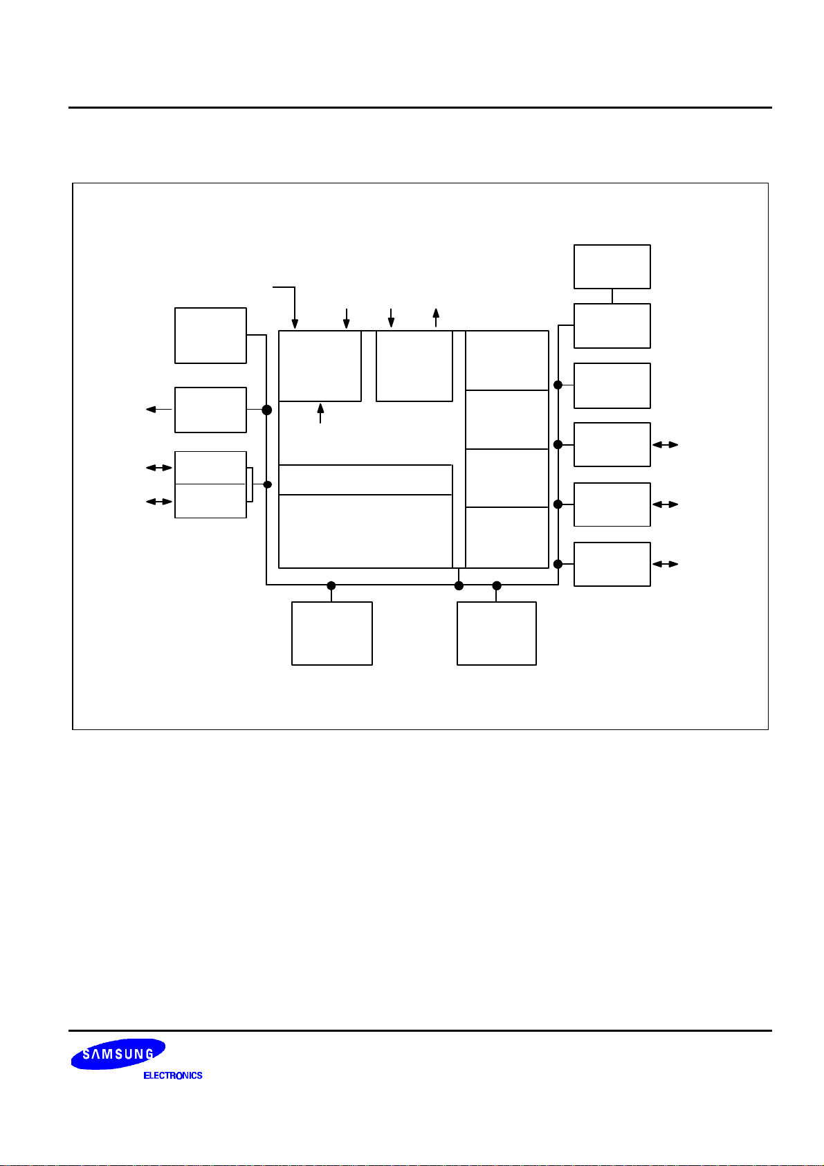
BLOCK DIAGRAM
Watchdog
Timer
DAO
P4.0–P4.3
P5.0–P5.3
INT0, INT1
8-bit
Timer/
Counter
D/A
Converter
I/O Port 4
I/O Port 5
RESET
Interrupt
Control
Block
Internal
Interrupts
Instruction Decoder
Arithmetic Logic Unit
X
IN
Clock
X
OUT
Stack
Pointer
Program
Counter
Program
Status
Word
Flags
Basic
Timer
Buzzer
I/O Port 0
I/O Port 1
P0.0/INT0
P0.1/INT1
P0.2/KS0
P0.3/KS1
P1.0/TCL0
P1.1/TCLO0
P1.2/CLO
P1.3/BUZ
512 x 4-bit
Data
Memory
4 K byte
Program
Memory
Figure 1-1. S3C7544 Simplified Block Diagram
I/O Port 2
P2.0
1-3
PRODUCT OVERVIEW S3C7544/P7544
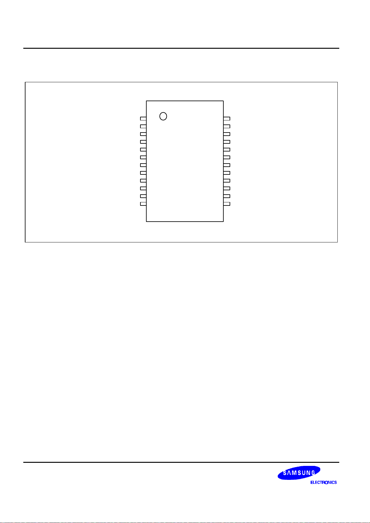
PIN ASSIGNMENTS
VSS
X
OUT
XIN
TEST
P0.0/INT0
DAO
P0.1/INT1
RESET
P0.2/KS0
P0.3/KS1
P1.0/TCL0
P1.1/TCLO0
1
2
3
4
5
6
7
8
9
10
11
12
24 SDIP-300
24 SOP-375
24
23
22
S3C7544
21
20
19
18
17
16
15
14
13
Figure 1-2. S3C7544 Pin Assignment Diagrams
VDD
P5.3
P5.2
P5.1
P5.0
P4.3
P4.2
P4.1
P4.0
P2.0
P1.3/BUZ
P1.2/CLO
1-4
S3C7544/P7544 PRODUCT OVERVIEW
PIN DESCRIPTIONS
Table 1-1. S3C7544 Pin Descriptions
Pin Name Pin Type Description Share Pin
P0.0
P0.1
P0.2
P0.3
P1.0
P1.1
P1.2
P1.3
P2.0 I/O 1-bit I/O port. 1- or 4-bit read/write and test is possible.
I 4-bit I/O port. 1- or 4-bit read/write and test is possible.
Pull-up resistors are assignable to input pins by software and are
automatically disabled for output pins. Pins are individually
configurable as input or output.
I/O 4-bit I/O port. 1- or 4-bit read/write and test is possible.
Pull-up resistors are assignable to input pins by software and are
automatically disabled for output pins. Pins are individually
configurable as input or output.
INT0
INT1
KS0
KS1
TCL0
TCLO0
CLO
BUZ
–
Pull-up resistors are assignable to input pins by software and are
automatically disabled for output pins.
P4.0–P4.3
I/O 4-bit I/O port. 1- or 4-bit read/write and test is possible.
–
Pins are individually configurable as input or output.
P5.0–P5.3
Pull-up resistors are assignable to input pins by software and are
automatically disabled for output pins.
The N-channel open drain or push-pull output can be selected by
software (1-bit unit).
INT0 I/O External interrupts with rising/falling edge detection P0.0
INT1 I/O External interrupts with rising/falling edge detection P0.1
KS0
KS1
I/O Quasi-interrupt input with falling edge detection P0.2
P0.3
TCL0 I/O External clock input for timer/counter P1.0
TCLO0 I/O Timer/counter clock output P1.1
CLO I/O CPU clock output P1.2
BUZ I/O 0.5, 1, 2, or 4 kHz frequency output at 4.19 MHz for buzzer sound P1.3
DAO O 8-bit D/A converter output –
V
DD
V
SS
RESET
– Main power supply –
– Ground –
I Reset signal –
TEST I Chip test input pin. Hold GND when the device is operating. –
XIN, X
OUT
– Crystal, ceramic oscillator signal for system clock –
1-5

PRODUCT OVERVIEW S3C7544/P7544
Table 1-2. Overview of S3C7544 Pin Data
SDIP Pin Numbers Share Pins I/O Type Reset Value Circuit Type
V
X
SS
OUT
, X
IN
– – – –
– – – –
TEST – I – –
P0.0, P0.1 INT0, INT1 I/O Input D-4
RESET
P0.2
P0.3
P1.0
P1.1
P1.2
P1.3
– I – B
KS0
I/O Input D-4
KS1
TCL0
I/O Input D-2
TCLO0
CLO
BUZ
P2.0 – I/O Input D-2
DAO – O Output –
P4.0–P4.3 – I/O Input E-2
P5.0–P5.3 – I/O Input E-2
V
DD
– – – –
1-6

S3C7544/P7544 PRODUCT OVERVIEW
PIN CIRCUIT DIAGRAMS
V
DD
P-Channel
IN
N-Channel
Figure 1-3. Pin Circuit Type A
V
DD
Data
Output
Disable
V
DD
P-Channel
N-Channel
Figure 1-5. Pin Circuit Type C
V
DD
Out
Pull-up
Resistor
IN
Schmitt Trigger
Figure 1-4. Pin Circuit Type B
Pull-up
Enable
Data
Output
Disable
Circuit
Type C
P-Channel
Figure 1-6. Pin Circuit Type D-2
In/Out
1-7
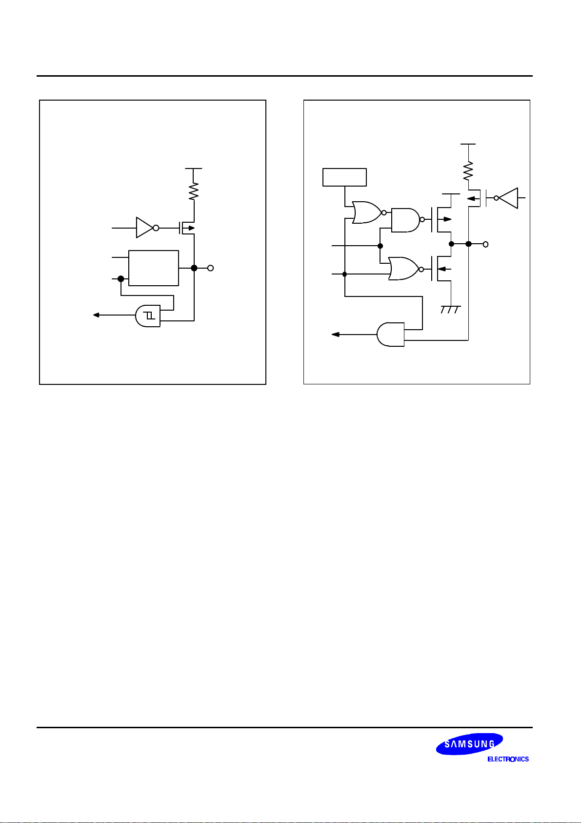
PRODUCT OVERVIEW S3C7544/P7544
V
DD
V
DD
PNE
V
DD
Pull-Up
Resistor
Pull-up
Enable
Data
Output
Circuit
Type C
P-Channel
Disable
Figure 1-7. Pin Circuit Type D-4
Resistor
Enable
In/Out
Data
In/Out
Output
Disable
Figure 1-8. Pin Circuit Type E-2
1-8

S3C7544/P7544 ELECTRICAL DATA
14 ELECTRICAL DATA
OVERVIEW
In this section, S3C7544 electrical characteristics are presented in tables and graphs. The information is
arranged in the following order:
Standard Electrical Characteristics
— Absolute maximum ratings
— D.C. electrical characteristics
— Main system clock oscillator characteristics
— Subsystem clock oscillator characteristics
— I/O capacitance
— A.C. electrical characteristics
— Operating voltage range
Miscellaneous Timing Waveforms
— A.C timing measurement point
— Clock timing measurement at X
— Clock timing measurement at XT
— TCL timing
— Input timing for RESET
— Input timing for external interrupts
— Serial data transfer timing
Stop Mode Characteristics and Timing Waveforms
— RAM data retention supply voltage in stop mode
— Stop mode release timing when initiated by RESET
— Stop mode release timing when initiated by an interrupt request
in
in
14-1
 Loading...