

Page 1
PLASMA DISPLAY TV
Chassis : D63A(N)
Model : PPM63H3X/XSF
PLASMA DISPLAY TV CONTENTS
1.
2.
3.
4.
5.
Specifications
Alignment and Adjustments
Exploded View and Parts List
Service Item
Schematic Diagrams
SERVICE
Manual
Page 2
This Service Manual is a property of Samsung Electronics Co.,Ltd.
Any unauthorized use of Manual can be punished under applicable
International and/or domestic law.
© Samsung Electronics Co., Ltd. MAY. 2004
Printed in Korea
AA82-01672A
ELECTRONICS
Page 3
Alignment and Adjustments
Samsung Electronics 2-1
2. Alignment and Adjustments
2-1 Service Mode
2-1-1 SERVICE MODE Entry Method (General Transmitter)
■ For the General Transmitter
1. Turn the power off and set to stand-by mode.
2. Press the buttons of the transmitter in this order; Info-Menu-Mute-Power or Mute-1-8-Power
to turn the set on.
3. The set turns on and enters service mode.
* If you fail to enter service mode, repeat steps 1 and 2 above.
2-1-2 Initial DISPLAY State of SERVICE MODE
2-1-2(A) OSD DISPLAY
2-1-2(B) B
utton Operations in SERVICE MODE
1. VSP9437-1 9. CXA2101
2. VSP9437-2 10. LOGIC
3. FLI2300 11. TP LOG-ASI
4. ASI500-1 12. Option
5. ASI500-2 13. CheckSum 0000
6. DNIe 14. Reset
7. AD9888
8. CXA2151
Release : 2003-07-12 T_NEW63MWW_1001
Menu
UP/DOWN Key
LEFT/RIGHT Key
Displays all menus
Cursor move to select items
Enable to increase and decrease the data of the selected items
SERVICE MAIN
Page 4
Alignment and Adjustments
2-2 Samsung Electronics
2-1-3 Factory Data Initial Value
VSP9437- 1 ( V IDEO )
V PEAKING 16
HPLL SPEED 00
RGB/YUV CONTRAST 41
RGB/YUV BRIGHTNESS 248
YUV SATCB 26
YUV SATCR 26
PAL B/G 01
PAL D/K 01
PAL I 01
SECAM B/G 27
SECAM D/K 27
SECAM L'/L 27
NTSC M 01
NTSC 4. 43 27
ASI5 00 I ( VIDEO / PC ,DVI )
R CONTRAST 3 2/30
G CONTRAST 32/30
B CONTRAST 32/30
R BRIGHTNESS 00
G BRIGHTNESS 00
B BRIGHTNESS 00
TEXT ALPHA 01
TEXT THRESHOLD 07
FILT ER ML 00
FILT ER MR 00
FILT ER FR 00
FILT ER MC 16
FILT ER UC 00
FILT ER LC 00
PAL 60 27
PAL M/N 01
PAL 01
SECAM 27
NTSC 01
NTSC 4. 43 27
PAL 60 27
NR 01
FILTER YPASS 00
R GAMMA 32
G GAMMA 32
B GAMMA 32
H POSITION 00
V POSITION 00
HSIZE 00
VSIZE 00
OVERSCAN R 50
OVERSCAN G 5 0
OVERSCAN B 5 0
VSP943 7 - 2
V PEAKING 16
HPLL SPEED 01
PAL 01
SECAM 27
NTSC 01
PAL AV 01
SECAM AV 27
NTSC AV 01
PIP R CONTRAST 32
PIP G CONTRAST 32
PIP B CONTRAST 32
PIP R BRIGHTNESS 00
PIP G BRIGHTNESS 00
PIP B BRIGHTNESS 00
PIP FILTER IC 00
PIP FILTER ML 00
PIP FILTER MR 00
PIP FILTER UC 00
F LI2 30 0
Y DELAY 0 5
C DELAY 1 2
CONTRAST 95
BRIG HTNESS 185
SATURATION 110
ASI 500 II
Page 5

Alignment and Adjustments
Samsung Electronics 2-3
DNIe (VIDEO / PC, DVI) AD98 8 8 (V IDEO / COMP/ PC)
BRIGHT OFFSET
CONTRA OFFSET
SCALE MAX Y
SCALE MIN Y
TH HPF
TH EDGE
NR SEL
CE UPPER
CE CUTOFF
CE GAIN
DCE GAIN
SKIN ON
CTI GAIN
DE NOISE GAIN
Attachment
Attachment
48
16
00
04/05
02
220/240
45
64/75
190/96
00
00/08
08/10
PICT URE 16
HUE 3 1
COLOR 16
BRIG HT 61
SHARPNESS 28
R-DRIVE 04
G-DRIVE 04
B-DRIVE 04
R-CUTOFF 32
G-CUTOFF 32
B-CUTOFF 32
TH CORING
PATT SEL
NOISE TH3
H CONT
V CONT
BLACK GAIN
WHITE GAIN
WTE GAIN
CTE GAIN
H SHARP GAIN
V SHARP GAIN
SHARPNESS
CLK DLY
H POSI
CXA210 1
SUB-BRIGHT 35
CR-OFFSET1 07
CB-OFFSET1 07
SUB-CONT 12
SUB-COL 08
SUB-HUE 08
R-Y/ R 13
R-Y/ B 15
G-Y/ R 12
G-Y/ B 04
02
00
100
32
32
375
375
300
176
127/48
127/48
100
07
14
R GAIN 127/190/127
GGAIN
BGAIN
R, CR OFFSET
G, Y OFFSET
B, CB OFFSET
127/213/127
127/206/127
54/79/54
54/34/54
54/75/54
VIDEO PATH PC
AUTO COLOR OFF
CXA2151
GAIN SEL 01
CB GAIN 07
CR GAIN 07
YGAIN 01
HFREQ 00
Page 6
Alignment and Adjustments
2-4 Samsung Electronics
LOGIC (PDP DRIVER)
R DRIVE
G DRIVE
B DRIVE
R CUTOFF
G CUTOFF
B CUTOFF
Attachment
Attachment
Attachment
Attachment
Attachment
Attachment
GAMMA 01
GTS SET 01
ERD MODE 01
RANDOM NOISE 01
DIFF FI LTE R 01
APC 01
APC SET 00
APC VALUE 127
TP LO G- ASI (TEST PAT LOGIC /SCALER)
LOG PATTERN 0 0
LOG HIGH LEVEL 00
LOG LOW LEVEL 00
ASI COLORBAR 00
ACTI VE V POS 12
ACTI VE H POS 19
V SYNC POS 03
H SYNC POS 32
V SYNC WIDTH 02
H SYNC WIDTH 12
OPTION
PIXEL SHIF T V
SHIFT TEST OFF
PIXEL NMBER 04
SHIFT L INE 04
SHIFT TIME 04
RGB DNIe OFF
DNIe DEMO OFF
DNIe THROUGH OFF
VIDEO MUTE 00
1366x768 ON
MDC ENABLE ON
LAST MEMORY ON
Attachment
■
W/B Data
IC
SNI
Logic
ITEM
Bright
Con t rast
RGain
GGain
BGain
RCutoff
GCutoff
BCutoff
Video ,S-VHS Component PC DVI
02
247
145
130
120
232
00
252
15
07
125
130
105
02
00
243
00
00
125
130
105
02
00
243
00
00
125
130
97
00
00
254
Page 7
Alignment and Adjustments
Samsung Electronics 2-5
Alignment and Adjustments
2-2 WHITE Balance Coordinates
2-2-1 White Balance Adjustment
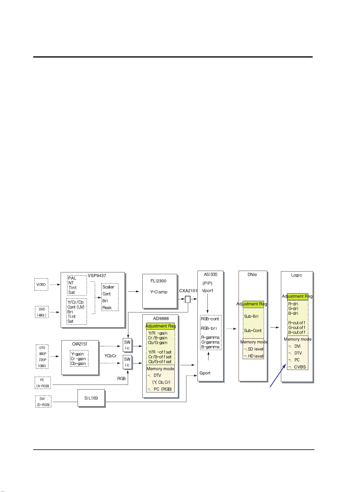
1. W/B Adjustment is required for the following four modes: DVI → DTV → PC → CVBS(VIDEO)
→ CVBS(VIDEO PIP)
2. Adjustment Method (DVI, DTV, PC : VG828, CVBS : Adjust RF signals to match the
Toshiba pattern (in-house signal)
! Adjust the target set by adjusting the panel logic and the video DNIe adjustment register in
register in order to determine the referential W/B of the panel with a DVI input, which
is the full digital path.
@ For DTV adjustment, adjust the adjustment register of ad9888 to align the DTV signal
to the DNIe and logic panel value which was fixed with a DVI adjustment so that they are
in effect considered to be the same signals. (At this time, do not adjust the gain of
AD9888
→ the Highlight W/B does not need to be adjusted since its deviation falls
within valid distribution range.)
# PC adjustment is same as DTV adjustment. (The offset can be applied to the values
obtained through DTV adjustment. However, additional adjustment is required for
Y, Cb, and Cr of DTV since PC processes R, G, and B signals.)
$ cvbs adjustment is performed with the Toshiba pattern (in-house signal) and differs
from the VG828 signals in the above three modes. Hence, it should be performed with
the same method of ! DVI adjustment.
% Finally, activate PIP in video mode, and repeat W/B adjustment.
❈ Thus, Micom saves the W/B data separately for each memory mode of the block
(See the block diagram given below) during W/B adjustment.
Micom can memorize the four modes
separately. However, under the current
adjustment guidelines, DTV and PC are
memorized with the same value during
DVI adjustment and CVBS is memorized
with a separate value.
Page 8
Alignment and Adjustments
2-6 Samsung Electronics
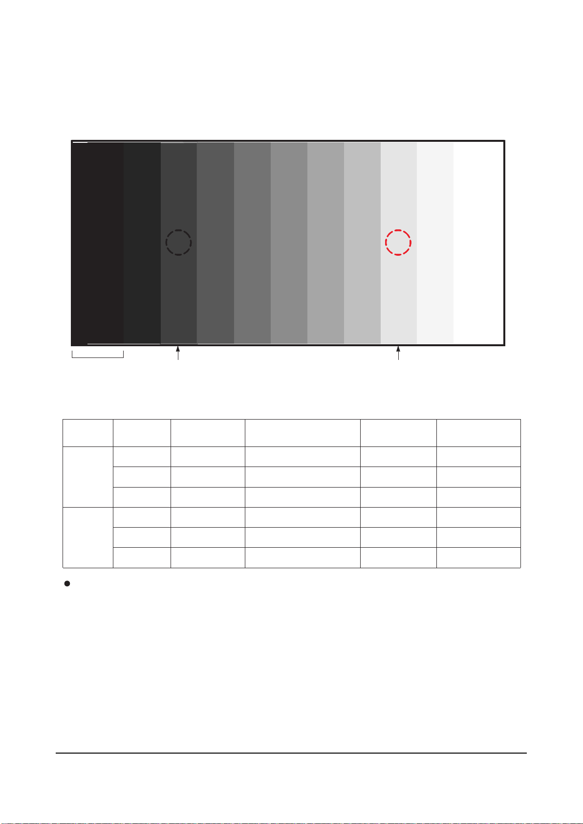
2-2-2 White Balance Coordinates by Mode
PedestalLevel Low Light
measure point
DVI
DTV COMPONENT
(480P, 720P,1080i
x 285 285 285 280
H/L
y 295
Y(fL) 31.5 20.0 31.5
25
295 295 295
x 285 285 285 285
L/L
y 295 295 295 300
Y(fL) 0.8 0.9 0.8 0.9
Pattern Used in Adjustment : 10 Steps Grayscalepattern
High Light
measure point
)
PC VIDEO
Page 9
Alignment and Adjustments
Samsung Electronics 2-7
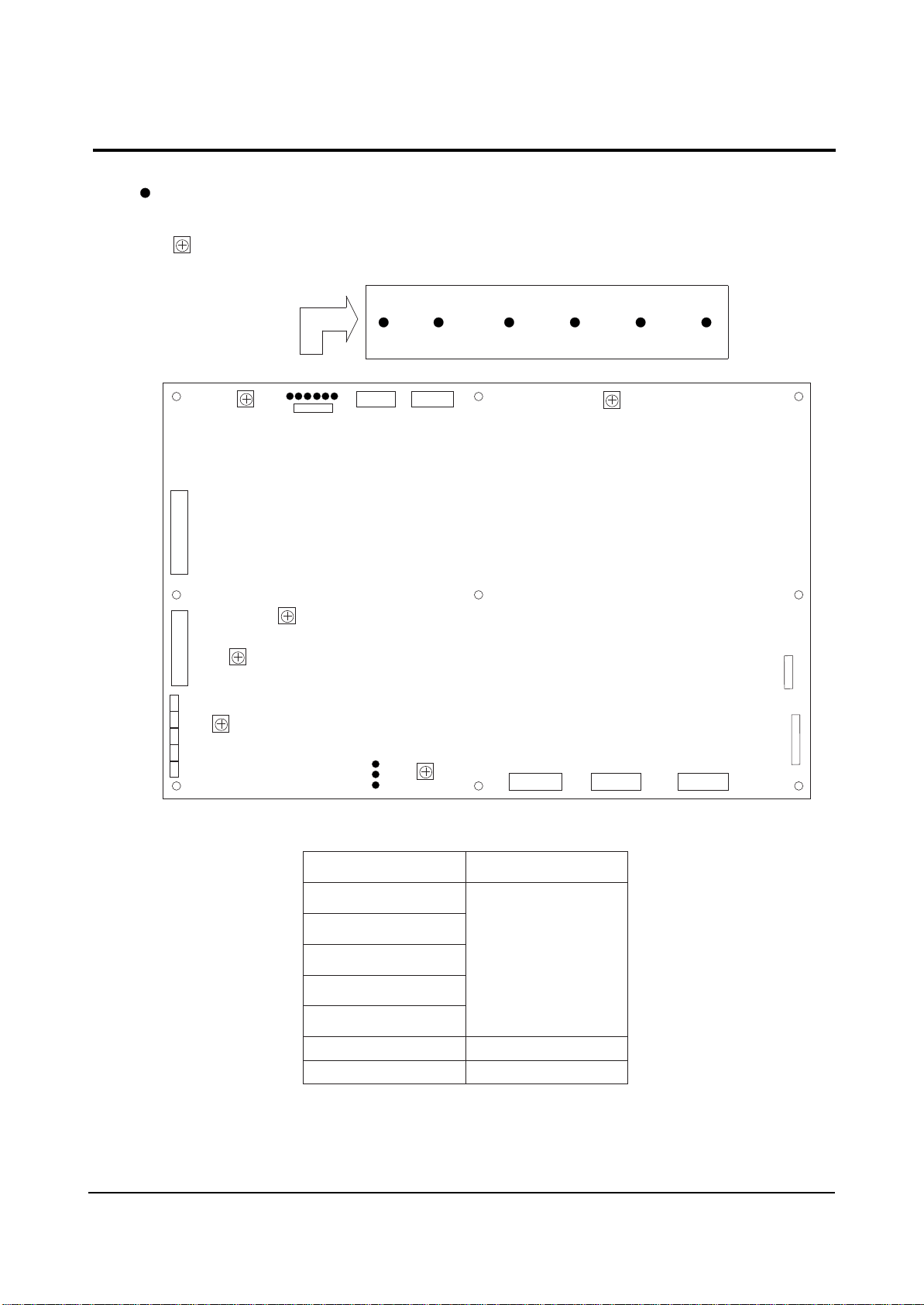
2-3 Voltage Adjustment
Tuning the variable resistor(VR) adjusts voltage
T:TestPoint
VR : Variable Resistor
VR8601
VS
CN804
VR8540
VE
T
CN830
CN806
Test Point
VSET VSCAN VE VA VS
CN811
VR8501
VA
SMPS-DC
CN805
VR8580
VSET
VR8560
VSCAN
VR8491
T
D5V
A6V
OUTPUT Voltage
VSCAN
D5V
VS
VSET
VE
VA
D5V +5V
A6V +6V
See the labels
attached on the
base chassis.
CN851B
CN852B
CN803CN802
CN801
Page 10

2-8 Samsung Electronics
MEMO
Page 11
Electrical Parts List
Samsung Electronics
4-1
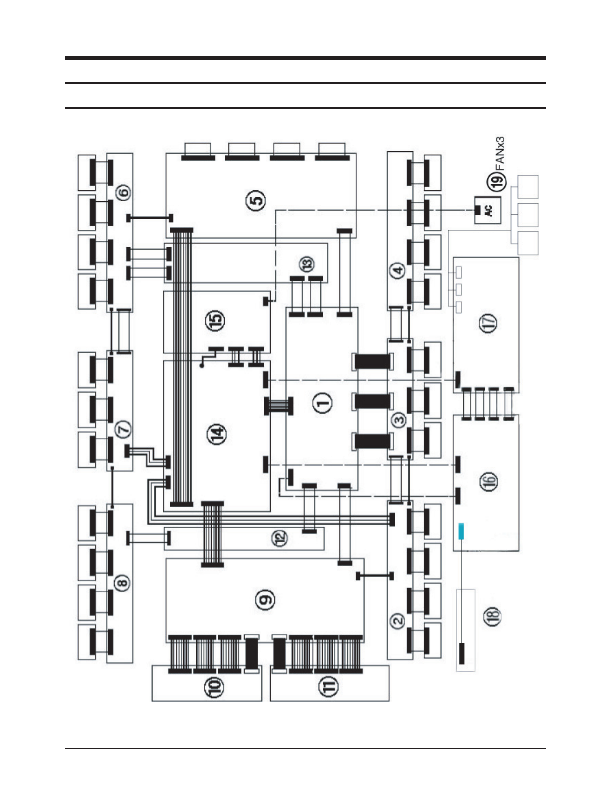
4. Service Item
4-1 Assy Board & Part List for Service
Page 12

Electrical Parts List
4-2
Samsung Electronics
SPECIFICATION
ASSY PDP P-LOGIC MAIN BOARD;M3,S63HW-XD0
LJ92-00683A,M3,S63HW-XD02,63HD D1.0,E BUFF,LJ92-00683A
BN96-00935A ASSY PDP P-MODULE;M3,S63HW-XD02,D55A,D2
CODE NO
BN96-00939A
BN96-00372A
DESCRIPTION
ASSY PDP P-MODULE
ASSY PDP P-PBA L MAIN
ASSY PDP P-E BUFF
1
NO
2
LJ92-00684A,M3,S63HW-XD02,63HD D1.0,F BUFF,LJ92-00684A
LJ92-00685A,M3,S63HW-XD02,63HD D1.0,G BUFF,LJ92-00685A
LJ92-00680A,M3,S63HW-XD02,63HD D1.0,X MAIN BOARD,LJ92-00680A
LJ92-00688A,M3,S63HW-XD02,63HD D1.0,J BUFF,LJ92-00688A
LJ92-00687A,M3,S63HW-XD02,63HD D1.0,I BUFF,LJ92-00687A
LJ92-00686A,M3,S63HW-XD02,63HD D1.0,H BUFF,LJ92-00686A
LJ92-00679A,M3,S63HW-XD02,63HD D1.0,Y MAIN BOARD,LJ92-00679A
LJ92-00681A,M3,S63HW-XD02,63HD D1.0,Y BUFF UP,LJ92-00681A
LJ92-00682A,M3,S63HW-XD02,63HD D1.0,Y BUFF DOWN,LJ92-00682A
LJ92-00652A,M3,S63HW-XD02,63HD D1.0,LOGIC SUB R,LJ92-00652A
LJ92-00653A,M3,S63HW-XD02,63HD D1.0,LOGIC SUB L,LJ92-00653A
,D54A,HD,NTSC,PAL,63 INCH
,D54A,HD,NTSC,PAL,63 INCH
BN96-00371A
BN96-00370A
BN96-00359A
BN96-00363A
BN96-00364A
BN96-00365A
BN96-00358A
BN96-00374A
BN96-00373A
BN96-00360A
BN96-00361A
BN96-00231A
ASSY PDP P-F BUFF
ASSY PDP P-G BUFF
ASSY PDP P-X MAIN BOARD
ASSY PDP P-J BUFF
ASSY PDP P-I BUFF
ASSY PDP P-H BUFF
ASSY PDP P-Y MAIN BOARD
ASSY PDP P-Y BUFF UP
ASSY PDP P-Y BUFF DOWN
ASSY PDP P-LOGIC SUB R
ASSY PDP P-LOGIC SUB L
ASSY PDP P-SMPS
3
4
5
6
7
8
9
101112131415161718
PPM63H3,D63A,NEWTON VMB SPD-63P3H,D57A,ALE
BN96-00232A
BN94-00532D
ASSY PDP P-SMPS,DC
ASSY PCB MISC-DIGITAL
G4020S05B2-RS,PBTP,UL94-Vo,Bracket,BN61-00624A
63INCH,T47%,1442*832,T3.8,0.15OHM
TM76,D61A,42,G6148,PPM42S3,EX
NL5MO,15P/15P,2990,1830MM,UL2
BN94-00449J PPM63H3,D63A,VMB,SH
BN94-00494D
BN31-00001A
BN67-00077A
BN59-00366A
BN39-00115A
ASSY PCB MISC-ANALOG
ASSY PCB MISC-CONTROL
FAN-ASSY
SCREEN-EMI,FILTER(GLASS)
REMOCON
CBF SIGNAL (D-SUB 15P)
19
PDP,9P/1P,UL2851#28,5000MM,UL2851,BLK,DSUB/STEREO PLUG,2C,SJ01-01-296
D54A/SPD-42P3S,UL1007#24,UL/CSA,2P,2000MM,#24,SME-00014,STRIP,BK,1007#24
SYNCMASTER,PIVOT,SAMSUNG
PPM42S3/50H3/63H3,RS232C-PROGRAM,Worldwide,CD-ROM
PPM42S3,EN/CHI,W/P100G,D61A,B5,VMB
AA39-00311A
BN39-00315A
BN59-00048A
CBF SIGNAL (MDC CABLE)
LEAD CONNECTOR (SEAKER CABLE)
S/W DRIVER-7.0 (PIVOT S/W)
3903-000082 DT,CN,IP3/YES(A),I(IEC C13/C14),250/250V,10/10A,BLK,1830MM,-,RVV300/500
BN59-00389A
BN68-00491A
S/W DRIVER (MDC S/W)
MANUAL USERS
CBF POWER CORD
ACCESSORY
ACCESSORY
ACCESSORY
ACCESSORY
ACCESSORY
ACCESSORY
ACCESSORY
ACCESSORY
Page 13

Electrical Parts List
Samsung Electronics
4-3
LOC.NO. CODE NO. SPEC Q'TY
D0254 AA32-00013B MODULE REMOCON;346HF5,38KHz,940mm,MESH,H 1
T0268 3903-000082 CBF-POWER CORD;DT,CN,IP3/YES(A),I(IEC C1 1
T0074 BN59-00366A REMOCON;TM76,D61A,42,G6148,PPM42S3,EX 1
T0132 BN94-00532D ASSY PCB MISC-DIGITAL;PPM63H3,D63A,NEWTO 1
T0145 BN94-00449J ASSY PCB MISC-ANALOG;PPM63H3,D63A,VMB,SH 1
T0098 BN94-00494D ASSY PCB MISC-CONTROL;SPD-63P3H,D57A,ALE 1
T0046 BN96-00231A ASSY PDP P-SMPS;,D54A,HD,NTSC,PAL,63 INC 1
T0046 BN96-00232A ASSY PDP P-SMPS,DC;,D54A,HD,NTSC,PAL,63 1
T0008 BN96-00302C ASSY COVER P-BACK SUB;63P3 VMB,AL T1.5,D 1
M0003 BN96-00303N ASSY COVER P-FRONT;63P3H(VMB),ASIA,ABS H 1
T0001 BN96-00308C ASSY COVER P-BACK;63P3 VMB,AL T1.5,DGM52 1
T0096 BN96-00358A ASSY PDP P-Y MAIN BOARD;LJ92-00679A,M3,S 1
T0073 BN96-00359A ASSY PDP P-X MAIN BOARD;LJ92-00680A,M3,S 1
T0297 BN96-00360A ASSY PDP P-LOGIC SUB R;LJ92-00652A,M3,S6 1
T0297 BN96-00361A ASSY PDP P-LOGIC SUB L;LJ92-00653A,M3,S6 1
T0118 BN96-00363A ASSY PDP P-J BUFF;LJ92-00688A,M3,S63HW-X 1
T0035 BN96-00364A ASSY PDP P-I BUFF;LJ92-00687A,M3,S63HW-X 1
T0034 BN96-00365A ASSY PDP P-H BUFF;LJ92-00686A,M3,S63HW-X 1
T0033 BN96-00370A ASSY PDP P-G BUFF;LJ92-00685A,M3,S63HW-X 1
T0032 BN96-00371A ASSY PDP P-F BUFF;LJ92-00684A,M3,S63HW-X 1
T0031 BN96-00372A ASSY PDP P-E BUFF;LJ92-00683A,M3,S63HW-X 1
T0047 BN96-00373A ASSY PDP P-Y BUFF DOWN;LJ92-00682A,M3,S6 1
T0048 BN96-00374A ASSY PDP P-Y BUFF UP;LJ92-00681A,M3,S63H 1
T0044 BN96-00935A ASSY PDP P-MODULE;M3,S63HW-XD02,D55A,D2. 1
T0037 BN96-00939A ASSY PDP P-LOGIC MAIN BOARD;M3,S63HW-XD0 1
Yon can search for the updated part code through ITSELF web site.
URL:http://itself.sec.samsung.co.kr
4-2 PPM63H3X/XSF
Page 14

4-4
Samsung Electronics
MEMO
Page 15

3. Exploded View & Parts List
3-1 PPM63H3X/XSF
Exploded View & Parts List
Samsung Electronics 3-1
1 BN96-00303N ASSY COVER P-FRONT;63P3H(VMB),ASIA,ABS H 1 M0003
1-1 BN64-00127N CABINET FRONT;63P3 VMB,ABS,HB,HF-1690H,W 1 T0003 S.N.A
1-2 BP64-00179A BADGE-BRAND;ALL,AL,T1.5,83,14,,BLK,SILIV 1 T0057 S.N.A
1-3 BP64-00045C KNOB CONTROL;P3,ABS,HB,WP1000 1 T0022 S.N.A
1-4 BN64-00074B WINDOW-REMOTE;42P3S,PMMA,,,,,,CLEAR 1 S.N.A
2 BN94-00494D ASSY PCB MISC-CONTROL;SPD-63P3H,D57A,ALE 1 T0098
3 6003-001489 SCREW-TAPTITE;BH,+,B,M4,L15,ZPC(KHAKI),S 3 T0081 S.N.A
4 BN67-00077A GLASS;63INCH,T47%,1442*832,T3.8,0.15OHM 1 S.N.A
5 BN96-00305B ASSY MISC P-FILTER TOP;SPD-63P3H,AL,T2.0 1 S.N.A
6 BN96-00306B ASSY MISC P-FILTER BTM;SPD-63P3H,AL,T2.0 1 S.N.A
7 BN96-00307B ASSY MISC P-FILTER SIDE;SPD-63P3H,AL,T2. 2 S.N.A
8 6003-001489 SCREW-TAPTITE;BH,+,B,M4,L15,ZPC(KHAKI),S 8 T0081 T0081
9 AA60-00110L SPACER-FILTER;63P3H,P/U FROM,1420,6.0,9. 2 T0918 S.N.A
10 AA60-00110M SPACER-FILTER;63P3H,P/U FROM,1420,6.0,9. 2 T0918 S.N.A
11 BN96-00935A ASSY PDP P-MODULE;M3,S63HW-XD02,D55A,D2. 1 T0044
12 BN72-00345A SPONGE;SPD-63P3H,SHIELD-FORM,14,14,225,P 1 S.N.A
13 BN63-00627A SHIELD-FUNCTION;SPD-63P3H,AL,T1.0 1 S.N.A
14 6003-001489 SCREW-TAPTITE;BH,+,B,M4,L15,ZPC(KHAKI),S 26 T0081 S.N.A
15 BN96-00231A ASSY PDP P-SMPS;,D54A,HD,NTSC,PAL,63 INC 1 T0046
16 BN96-00232A ASSY PDP P-SMPS,DC;,D54A,HD,NTSC,PAL,63 1 T0046
17 BN96-00359A ASSY PDP P-X MAIN BOARD;LJ92-00680A,M3,S 1 T0073
18 BN96-00939A ASSY PDP P-LOGIC MAIN BOARD;M3,S63HW-XD0 1 T0037
19 BN96-00358A ASSY PDP P-Y MAIN BOARD;LJ92-00679A,M3,S 1 T0096
20 BN96-00302C ASSY COVER P-BACK SUB;63P3 VMB,AL T1.5,D 1 T0008
21 6003-001489 SCREW-TAPTITE;BH,+,B,M4,L15,ZPC(KHAKI),S 3 T0081 S.N.A
22 6001-001786 SCREW-MACHINE;TH,+,M4,L8,ZPC(BLK),SWRCH1 4 CCM1 S.N.A
23 BN31-00001A FAN-ASSY;G4020S05B2-RS,PBTP,UL94-Vo,Brac 3 T0243
24 6006-001132 SCREW-MACHINE;WSP,PH,+,M3,L8,NI PLT,SWRC 8 EL013 S.N.A
25 BN94-00532D ASSY PCB MISC-DIGITAL;PPM63H3,D63A,NEWTO 1 T0132
26 BN94-00449J ASSY PCB MISC-ANALOG;PPM63H3,D63A,VMB,SH 1 T0145
27 6006-001132 SCREW-MACHINE;WSP,PH,+,M3,L8,NI PLT,SWRC 8 CCM1 S.N.A
28 2901-001263 FILTER-EMI AC LINE;250V,10A,-,2200PF,50X 1 FT532
29 6006-001112 SCREW-MACHINE;WP,PH,+,M8,L16,ZPC(BLK),SW 2 CCM1
30 BN96-00308C ASSY COVER P-BACK;63P3 VMB,AL T1.5,DGM52 1 T0001
31 6003-001489 SCREW-TAPTITE;BH,+,B,M4,L15,ZPC(KHAKI),S 11 T0081 S.N.A
32 6001-001786 SCREW-MACHINE;TH,+,M4,L8,ZPC(BLK),SWRCH1 11 CCM1 S.N.A
33 6006-001112 SCREW-MACHINE;WP,PH,+,M8,L16,ZPC(BLK),SW 6 CCM1
34 BN96-00304F ASSY MISC P-BRACKET TERMINAL;63P3,AL,1.5 1 S.N.A
35 6001-001786 SCREW-MACHINE;TH,+,M4,L8,ZPC(BLK),SWRCH1 8 CCM1 S.N.A
36 BN64-00153B DECORATION;SPD-63P3H,ABS+PC,3.0,5V 1 S.N.A
37 6001-001786 SCREW-MACHINE;TH,+,M4,L8,ZPC(BLK),SWRCH1 4 CCM1 S.N.A
38 6003-001489 SCREW-TAPTITE;BH,+,B,M4,L15,ZPC(KHAKI),S 7 T0081 S.N.A
No Code No Description;Specification Q’ty Loc.No. S.N.A
Yon can search for the updated part code through ITSELF web site.
URL:http://itself.sec.samsung.co.kr
Page 16

COMPONENT1
Connector
Analog - Digital Board
Video IN
Video/S-Video Sound
S-Video
CXA2151Q
IC103
TP02
TP03
TP01
5. Schematic Diagrams
Samsung Electronics
Schematic Diagrams
5-1
5-1 ANALOG 1
TP01
TP02
TP03
This Document can not be used without Samsung’s authorization.
Page 17

Schematic Diagrams
5-2 Samsung Electronics
5-2 ANALOG 2
This Document can not be used without Samsung’s authorization.
R246 R247
TILT SENSOR
3D COMB FILTER
To DC FAN
FAN PART
50"
Page 18

Samsung Electronics
Schematic Diagrams
5-3
5-3 ANALOG 3
TP04
TP05
TP06
TP07
This Document can not be used without Samsung’s authorization.
TP05
TP04
From SMPS Board
TP06
MONITOR OUT VIDEO
TP07
External Speaker
MONITOR OUT SOUND
Page 19

Schematic Diagrams
5-4 Samsung Electronics
5-4 CONTROL
This Document can not be used without Samsung’s authorization.
AA32-00013B
Page 20

Samsung Electronics
Schematic Diagrams
5-5
5-5 SMPS 1
This Document can not be used without Samsung’s authorization.
Page 21

Schematic Diagrams
5-6 Samsung Electronics
5-6 SMPS 2
This Document can not be used without Samsung’s authorization.
Page 22

Samsung Electronics
Schematic Diagrams
5-7
5-7 SMPS 3
This Document can not be used without Samsung’s authorization.
Page 23

Schematic Diagrams
5-8 Samsung Electronics
5-8 SMPS 4
This Document can not be used without Samsung’s authorization.
Page 24

Samsung Electronics
Schematic Diagrams
5-9
5-9 SMPS 5
This Document can not be used without Samsung’s authorization.
Page 25

Schematic Diagrams
5-10 Samsung Electronics
5-10 SMPS 6
This Document can not be used without Samsung’s authorization.
Page 26

Samsung Electronics
Schematic Diagrams
5-11
5-11 SMPS 7
This Document can not be used without Samsung’s authorization.
Page 27

Schematic Diagrams
5-12 Samsung Electronics
5-12 DIGITAL 1
TP08
TP09
TP10
This Document can not be used without Samsung’s authorization.
Analog - Digital board
Connector
42 SD
42 HD
50,63 HD
PC(D-SUB&DVI) SOUND
TP10
TP08
TP09
Page 28

Samsung Electronics
Schematic Diagrams
5-13
5-13 DIGITAL 2
TP20
TP21
TP22
TP23
TP24
This Document can not be used without Samsung’s authorization.
PC D-SUB
BNC Connector
TP23
TP24
From SMPS board
ANALOG EDID EPROM
TP22
TP21
TP20
Page 29

Schematic Diagrams
5-14 Samsung Electronics
5-14 DIGITAL 3
This Document can not be used without Samsung’s authorization.
Page 30

Samsung Electronics
Schematic Diagrams
5-15
5-15 DIGITAL 4
This Document can not be used without Samsung’s authorization.
DVI Connector
DIGITAL EDID EPROM
Page 31

Samsung Electronics 5-16
TP11
TP12
TP13
TP14
TP16
TP19
TP17
TP18
TP15
Schematic Diagrams
5-16 DIGITAL 5
TP11
TP12
TP13
TP14
TP15
TP16
TP17
TP18
TP19
This Document can not be used without Samsung’s authorization.
Page 32

5-17
Schematic Diagrams
Samsung Electronics
Flash Memory
USER EPROM (256K)
B12 : 1204-002105
RS232C IN
From Remote Control board
Flash Memory Download
RS232C OUT
TP26
TP25
5-17 DIGITAL 6
TP26
TP25
This Document can not be used without Samsung’s authorization.
Page 33

Samsung Electronics
Schematic Diagrams
5-18
TP27
TP28
5-18 DIGITAL 7
TP28TP27
This Document can not be used without Samsung’s authorization.
Page 34

5-19
Schematic Diagrams
Samsung Electronics
LVDS Connector
5-19 DIGITAL 8
This Document can not be used without Samsung’s authorization.
Page 35

Specifications
Samsung Electronics 1-1
1. Specifications
MODEL
Display
Display
Screen Size
Voltage
Power Consumption
Number of Pixels
External Control
AUDIO Input
AUDIO Output
VIDEO Input
VIDEO Output
Dimensions
Weight
PPM63H3
1503.4(W) x 89(D) x 893.8(H) mm / 59.15(W) x 3.5(D) x 35.19(H) inches
69 Kg (without stand)
63 Inches
AC 120V, 60Hz / AC 100-250V, 50/60Hz
630 Watts
1366(H) X 768(V)
RS-232C IN(Mini jack), RS-232C OUT(D-SUB 9P)
VIDEO / S-VIDEO
COMPONENT 1
COMPONENT 2
RGB(PC) 1/2
DVI
External Speaker (10W+10W)
Audio Output (L/R RCA)
VIDEO
S-VIDEO
COMPONENT 1 - 480i / 480p / 720p / 1080i
COMPONENT 2/RGB2(PC) IN (BNC, 5P, 480i~1080i, VGA~XGA)
RGB1(PC1) - D-SUB 15P
DVI
Monitor Output (RCA)
Page 36

1-2 Samsung Electronics
MEMO
 Loading...