

Samsung Electronics 7-1
IC Internal Diagram
7. IC Internal Diagram
7-1 74LV245 ; SIC6
Philips Semiconductors Product specification
74LV245Octal bus transceiver (3-State)
2
1998 Apr 20 853–1931 19258
FEATURES
• Wide operating voltage: 1.0 to 5.5 V
• Optimized for low voltage applications: 1.0 to 3.6 V
• Accepts TTL input levels between V
CC
= 2.7 V and V
CC
= 3.6 V
• Typical V
OLP
(output ground bounce) < 0.8 V at V
CC
= 3.3 V,
T
amb
= 25°C
• Typical V
OHV
(output VOH undershoot) > 2 V at V
CC
= 3.3 V,
T
amb
= 25°C
• Output capability: bus driver
• I
CC
category: MSI
DESCRIPTION
The 74LV245 is a low-voltage Si-gate CMOS device and is pin and
function compatible with 74HC/HCT245.
The 74LV245 is an octal transceiver featuring non-inverting 3-State
bus compatible outputs in both send and receive directions. The
74LV245 features an output enable (OE
) input for easy cascading
and a send/receive (DIR) input for direction control. OE
controls the
outputs so that the buses are effectively isolated.
QUICK REFERENCE DATA
GND = 0 V; T
amb
= 25°C; tr = t
f
≤ 2.5 ns
SYMBOL
PARAMETER CONDITIONS TYPICAL UNIT
t
PHL/tPLH
Propagation delay
An to Bn; Bn to A
n
CL = 15 pF;
VCC = 3.3 V
7.0 ns
C
I
Input capacitance 3.5 pF
C
I/O
Input/output capacitance 10 pF
C
PD
Power dissipation capacitance per buffer
VCC = 3.3 V
VI = GND to VCC, note 1
40 pF
NOTE:
1. C
PD
is used to determine the dynamic power dissipation (PD in µW)
P
D
= CPD V
CC
2
fi )ȍ (CL V
CC
2
fo) where:
f
i
= input frequency in MHz; CL = output load capacitance in pF;
f
o
= output frequency in MHz; VCC = supply voltage in V;
ȍ (C
L
V
CC
2
fo) = sum of the outputs.
ORDERING INFORMATION
PACKAGES TEMPERATURE RANGE OUTSIDE NORTH AMERICA NORTH AMERICA PKG. DWG. #
20-Pin Plastic DIL –40°C to +125°C 74LV245 N 74LV245 N SOT146-1
20-Pin Plastic SO –40°C to +125°C 74LV245 D 74LV245 D SOT163-1
20-Pin Plastic SSOP Type II –40°C to +125°C 74LV245 DB 74LV245 DB SOT339-1
20-Pin Plastic TSSOP Type I –40°C to +125°C 74LV245 PW 74LV245PW DH SOT360-1
PIN DESCRIPTION
PIN NUMBER SYMBOL FUNCTION
1 DIR Direction
2, 3, 4, 5,
6, 7, 8, 9
A0 to A7Data inputs/outputs
10 GND Ground (0 V)
18, 17, 16, 15,
14, 13, 12, 11
B0 to B7Data inputs/outputs
19 OE Output enable input (active LOW)
20 V
CC
Positive supply voltage
FUNCTION TABLE
INPUTS INPUTS/OUTPUT
OE DIR A
n
B
n
L L A = B Inputs
L H Inputs B = A
H X Z Z
NOTES:
H = HIGH voltage level
L = LOW voltage level
X = don’t care
Z = high impedance OFF-state
7-2 Samsung Electronics
IC Internal Diagram
Philips Semiconductors Product specification
74LV245Octal bus transceiver (3-State)
1998 Apr 20
3
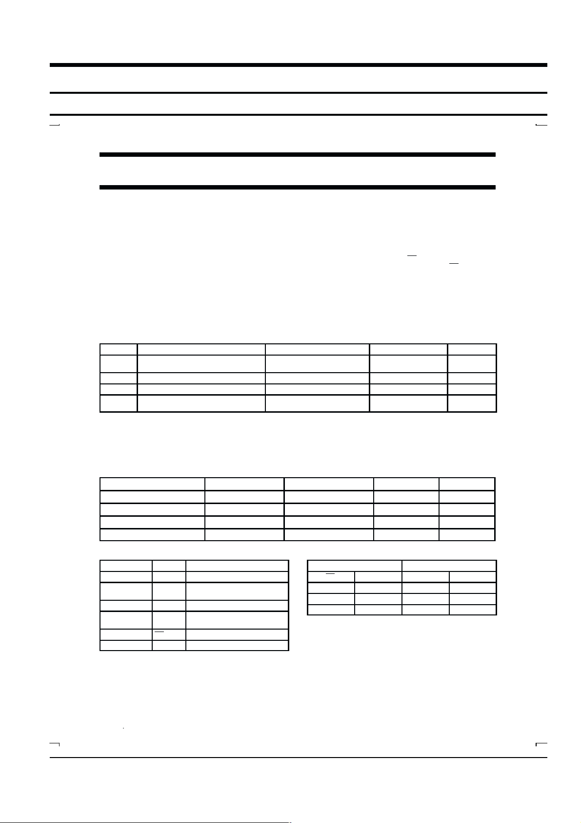
PIN CONFIGURATION
SV00624
1
2
3
4
5
6
7
8
9
10
20
19
18
17
16
15
14
13
12
11
DIR
A
0
A
1
A
2
A
3
A
4
A
5
A
6
A
7
GND
B
7
B
6
B
5
B
4
B
3
B
2
B
1
B
0
OE
V
CC
LOGIC SYMBOL (IEEE/IEC)
SV00626
G3
3EN1
3EN2
19
1
1
2
182
3
17
4
16
5
15
6
14
7
13
8
12
9
11
LOGIC SYMBOL
5
SV00625
A
0
DIR
B
0
OE
A
1
B
1
A
2
B
2
A
3
B
3
A
4
B
4
A
5
B
5
A
6
B
6
A
7
B
7
1
2
3
4
6
7
8
9
19
18
17
16
15
14
13
12
11
Samsung Electronics 7-3
IC Internal Diagram
7-2 74LV244 ; SIC7
Philips Semiconductors Product specification
74LV244Octal buffer/line driver (3-State)
2
1998 May 20 853–1924 19420
FEATURES
• Wide operating voltage: 1.0 to 5.5 V
• Optimized for low voltage applications: 1.0 to 3.6 V
• Accepts TTL input levels between V
CC
= 2.7 V and V
CC
= 3.6 V
• Typical V
OLP
(output ground bounce) < 0.8 V at V
CC
= 3.3 V,
T
amb
= 25°C
• Typical V
OHV
(output VOH undershoot) > 2 V at V
CC
= 3.3 V,
T
amb
= 25°C
• Output capability: bus driver
• I
CC
category: MSI
DESCRIPTION
The 74LV244 is a low-voltage Si-gate CMOS device and is pin and
function compatible with 74HC/HCT244.
The 74LV244 is an octal non-inverting buffer/line driver with 3-State
outputs. The 3-State outputs are controlled by the output enable
inputs 1OE
and 2OE. A HIGH on nOE causes the outputs to
assume a high impedance OFF-state. The 74LV244 is identical to
the 74LV240 but has non-inverting outputs.
QUICK REFERENCE DATA
GND = 0 V; T
amb
= 25°C; tr = t
f
≤ 2.5 ns
SYMBOL
PARAMETER CONDITIONS TYPICAL UNIT
t
PHL/tPLH
Propagation delay
1A
n
to 1Yn;
2A
n
to 2Y
n
CL = 15 pF;
V
CC
= 3.3 V
8.0 ns
C
I
Input capacitance 3.5 pF
C
PD
Power dissipation capacitance per buffer
VCC = 3.3 V
V
I
= GND to V
CC
1
35 pF
NOTE:
1. C
PD
is used to determine the dynamic power dissipation (PD in µW)
P
D
= CPD V
CC
2
fi )ȍ (CL V
CC
2
fo) where:
f
i
= input frequency in MHz; CL = output load capacitance in pF;
f
o
= output frequency in MHz; VCC = supply voltage in V;
ȍ (C
L
V
CC
2
fo) = sum of the outputs.
ORDERING INFORMATION
PACKAGES TEMPERATURE RANGE OUTSIDE NORTH AMERICA NORTH AMERICA PKG. DWG. #
20-Pin Plastic DIL –40°C to +125°C 74LV244 N 74LV244 N SOT146-1
20-Pin Plastic SO –40°C to +125°C 74LV244 D 74LV244 D SOT163-1
20-Pin Plastic SSOP Type II –40°C to +125°C 74LV244 DB 74LV244 DB SOT339-1
20-Pin Plastic TSSOP Type I –40°C to +125°C 74LV244 PW 74LV244PW DH SOT360-1
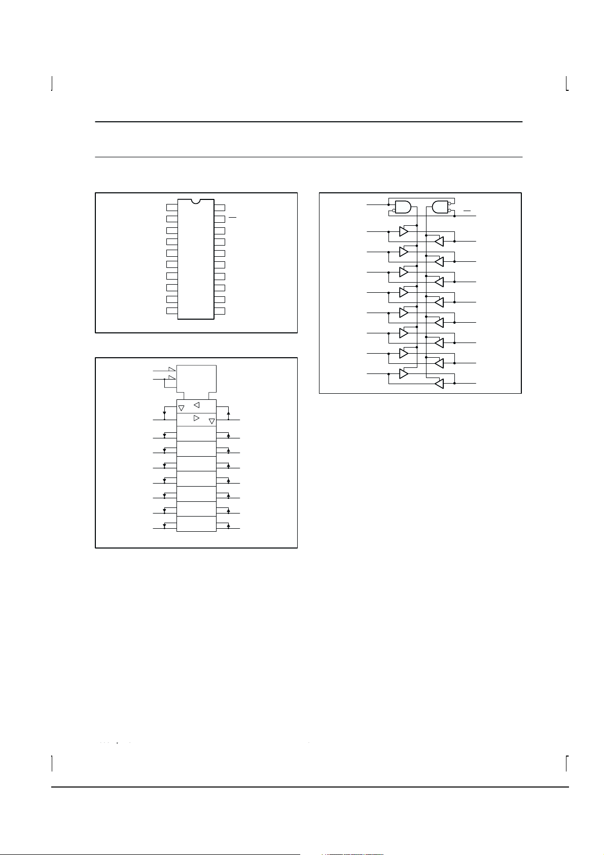
PIN CONFIGURATION
SV00620
1
2
3
4
5
6
7
8
9
10
20
19
18
17
16
15
14
13
12
11
1OE
1A
0
2Y
0
1A
1
2Y
1
1A
2
2Y
2
1A
3
2Y
3
GND
2A
3
1Y
3
2A
2
1Y
2
2A
1
1Y
1
2A
0
1Y
0
2OE
V
CC
LOGIC SYMBOL
SV00621
1Y
0
2Y
0
18
3
1Y
1
2Y
1
16
5
1Y
2
2Y
2
14
7
1Y
3
2Y
3
12
9
1A
0
2A
0
2
17
1A
1
2A
1
4
15
1A
2
2A
2
6
13
1A
3
2A
3
8
11
1OE1
2OE19
7-4 Samsung Electronics
IC Internal Diagram
Philips Semiconductors Product specification
74LV244Octal buffer/line driver (3-State)
1998 May 20
3
PIN DESCRIPTION
PIN
NUMBER
SYMBOL FUNCTION
1 1OE Output enable input (active LOW)
2, 4, 6, 8 1A0 to 1A3Data inputs
3, 5, 7, 9 2Y0 to 2Y3Bus outputs
10 GND Ground (0 V)
17, 15, 13, 11 2A0 to 2A3Data inputs
18, 16, 14, 12 1Y0 to 1Y3Bus outputs
19 2OE Output enable input (active LOW)
20 V
CC
Positive supply voltage
LOGIC SYMBOL (IEEE/IEC)
SV00666
18
16
14
12
2
4
6
8
EN
1
9
7
5
3
11
13
15
17
EN
19
FUNCTIONAL DIAGRAM
SV00622
2Y03
2Y
1
5
2Y
2
7
2Y
3
9
2A
0
17
2A
1
15
2A
2
13
2A
3
11
2OE
19
1Y018
1Y
1
16
1Y
2
14
1Y
3
12
1A
0
2
1A
1
4
1A
2
6
1A
3
8
1OE
1
FUNCTION TABLE
INPUTS OUTPUT
nOE nA
n
nY
n
L L L
L H H
H X Z
NOTES:
H = HIGH voltage level
L = LOW voltage level
X = don’t care
Z = high impedance OFF-state
Samsung Electronics 7-5
IC Internal Diagram
7-3 DAC3550A ; IC2
DAC 3550A
MICRONAS INTERMETALL 3
Stereo Audio DAC
1. Introduction
The DAC 3550A is a single-chip, high-precision, dual
digital-to-analog converter designed for audio applications. The employed conversion technique is based on
oversampling with noise-shaping.
With MICRONAS INTERMETALL’s unique multibit
sigma-delta technique, less sensitivity to clock jitter,
high linearity, and a superior S/N ratio has been
achieved. The DAC 3550A is controlled via I
2
C bus.
Digital audio input data is received by a versatile I
2
S
interface. The analog back-end consists of internal
analog filters and op amps for cost-effective additional
external sound processing. The DAC 3550A provides
line-out, headphone/speaker amplifiers, and volume
control. Moreover, mixing additional analog audio
sources to the D/A-converted signal is supported.
The DAC 3550A is designed for all kinds of applications in the audio and multimedia field, such as:
MPEG players, CD players, DVD players, CD-ROM
players, etc. The DAC 3550A ideally complements the
MPEG 1/2 layer 2/3 audio decoder MAS 3507D.
No crystal required for standard applications with
sample rates from 32 to 48 kHz. Crystal required
only for automatic sample rate detection below 32 kHz,
MPEG mode (refer to Section 2.10), and use of clock
output CLKOUT.
1.1. Main Features
– no master main input clock required
– integrated stereo headphone amplifier and mono
speaker amplifier
– SNR of 103 dBA
– I
2
C bus, I2S bus
– internal clock oscillator
– full-feature mode by I
2
C control (three selectable
subaddresses)
– reduced feature mode for non-I
2
C applications
– continuous sample rates from 8 kHz to 50 kHz
– analog deemphasis for 44.1 kHz
– analog volume and balance: +18…
75 dB and mute
– oversampling and multibit noise-shaping technique
– THD better than 0.01 %
– two additional analog stereo inputs (AUX) with
source selection and mixing
– supply range: 2.7 V…5.5 V
– low-power mode
– additional line-out
– on-chip op amps for cost-effective external analog
sound processing
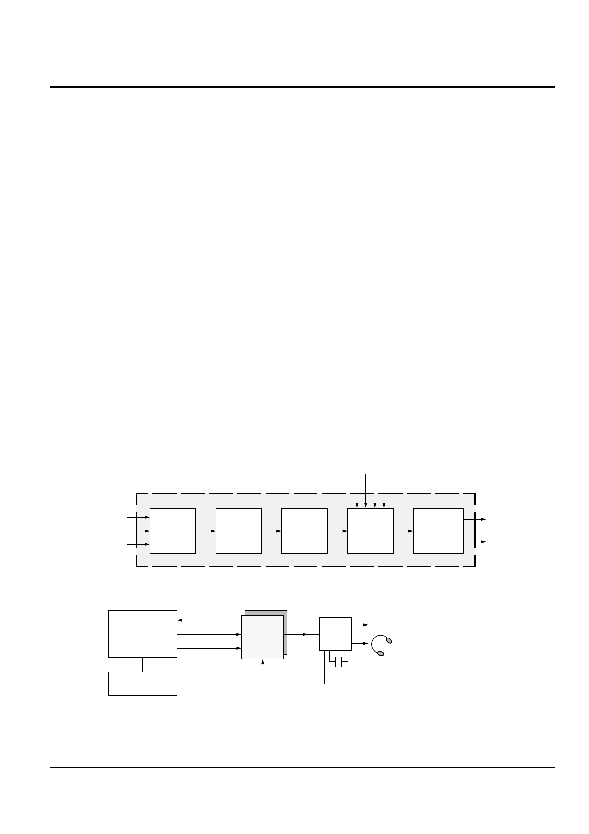
Fig. 1–1: Block diagram of the DAC 3550A
Fig. 1–2: Typical application: MPEG Layer 3 Player
WSI
CLI
DRI
OUTL
OUTR
Inter-
DAC
Input
Select
polation
Filter
Vol ume
and
Headphone
Amplifier
I2S
Analog Inputs
and
Mixing
MAS
ROM, CD-ROM,
RAM, Flash Mem. ..
DAC
Host
3507D
3550A
(PC, Controller)
I2S
line out
demand signal
MPEG clock
MPEG bit str eam
CLKOUT
14.725 MHz
7-6 Samsung Electronics
IC Internal Diagram
DAC 3550A
4 MICRONAS INTERMETALL
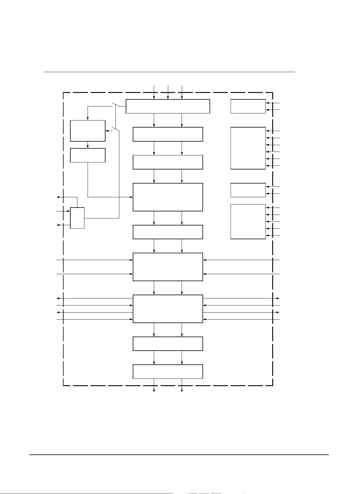
Fig. 1–3: Block diagram of the DAC 3550A
3rd-order Noise Shaper
I2S
Input Select
Interpolation Filter
Variable S & H
Osc.
Postfilter Op Amps
Analog Volume
Headphone Amplifier
Digital Supply
Analog
Control
I2C
Analog Low-pass Filter
Sample Rate
PLL
&
Multibit DAC
Deemphasis Op Amps
Vdd
Vss
AVDD0
AVDD1
AVSS0
AVSS1
VREF
AGNDC
SDA
SCL
PORQ
DEECTRL
MCS1
MCS2
AUX1R
AUX2R
DEEMR
FOPR
FOUTR
FINR
OUTROUTL
FINL
FOUTL
DEEML
AUX2L
AUX1L
XTO
XTI
CLKOUT
CLI DAI WSI
TESTEN
Switch Matrix
FOPL
Line-Out
9
10
3
2
44
1
16
15
27
26
19
21
20
32
30
35
42
41
43
18
17
57
39
37
38
34
31
29
12
13
14
23 24 25
Detection
Supply
Samsung Electronics 7-7
IC Internal Diagram
DAC 3550A
MICRONAS INTERMETALL 5
2. Functional Description
2.1. I
2
SInterface
The I
2
S interface is the digital audio interface between
the DAC 3550A and external digital audio sources
such as CD/DAT players, MPEG decoders etc. It covers most of the I
2
S-compatible formats.
All modes have two common features:
1. The MSB is left justified to an I
2
S frame identifica-
tion (WSI) transition.
2. Data is valid on the rising edge of the bit clock CLI.
16-bit mode
In this case, the bit clock is 32
× fs
audio
. Maximum
word length is 16 bit.
32-bit mode
In this case, the bit clock is 64
× fs
audio
. Maximum
word length is 32 bit.
Automatic Detection
No I
2
C control is required to switch between 16- and
32-bit mode. It is recommended to switch the
DAC 3550A into mute position during changing
between 16- and 32-bit mode.
For high-quality audio, it is recommended to use the
32-bit mode of the I
2
S interface to make use of the full
dynamic range (if more than 16 bits are available).
Left-Right Selection
Standard I
2
S format defines an audio frame always
starting with left channel and low-state of WSI. However, I
2
C control allows changing the polarity of WSI.
Delay Bit
Standard I
2
S format requires a delay of one clock
cycle between transitions of WSI and data MSB. In
order to fit other formats, however, this characteristic
can be switched off and on by I
2
C control.
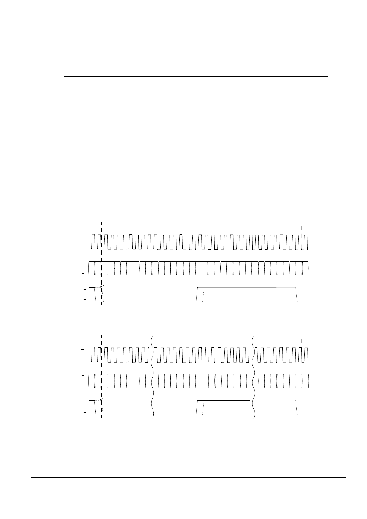
Fig. 2–1: I
2
S 16-bit mode (LR_SEL=0)
Fig. 2–2: I
2
S 32-bit mode (LR_SEL=0) Note: Volume mute should be applied before changing
I
2
S mode in order to avoid audible clicks.
CLI
DAI
V
h
V
l
WSI
left 16-bit audio sample
right 16-bit audio sample
1514131211109876543210
13 12 11 1098
76543210
15
14
V
h
V
l
V
h
V
l
programmable delay bit
CLI
DAI
V
h
V
l
WSI
left 32-bit audio sample
right 32-bit audio sample
29 28 27 26 25 24
76543210
31
30
V
h
V
l
V
h
V
l
programmable delay bit
29 28 27 26 25 24
76543210
31
30
 Loading...