

Page 1

Circuit Description
Samsung Electronics
Service Manual
12-1
12
12. Circuit Description
12.1 Engine Controller
The engine controller module consists of a motor controller, a PWM controller, a LSU I/F controller, and an ADC I/F
controller.
12.1.1 Heater Control
The heat lamp radiates heat by using AC power. The AC power is a TRIAC (a semiconductor switch device) which
controls a switch. The ‘ON/OFF’ control is completed by turning on/off a gate of the TRIAC through a photo TRIAC
which is insulation part.
If explaining more detail about the AC control part, it consists of passive circuit ; therefore, it turns on/off the heater
by receiving the signal from the engine control part. If the heater on signal is turned on at the engine, electricity flows
in as the LED of the PC1 (Photo TRIAC) is connected. Then, it emits light.
By this light, the TRIAC unit, a light receiving unit, becomes on, and electricity is supplied to the gate of the TRIAC.
Then, the TRIAC is turned on. As a result, AC current flows in a heat lamp, and the heat lamp radiates heat.
On the other contrary, if the signal is turned off, the PC1 becomes off, and the TRIAC is turned off due to no electricity at the gate of the TRIAC. Consequently, the heat lamp is turned off.
Special Feature of TRIAC (THY 1): 16A, 600V SWITCHING
Phototriac Coupler (PC3)
Turn On If Current: 15mA~50mA(Design: 16mA)
High Repeive Peak Off State Voltage: Min 600V
Vcc
Vcc
Vcc
R3
C2
1nF
R1
E
R5
5.6K
TR2 KSC
1008-Y
R4
BD1
Rs
C
TR1
KSC
1008-Y
BD2
3
C1
10nF
B
THERMISTOR
CN1
D1
914T1
D2
914T1
IC1
LM393D
R6
5.6K
R7
1K
R2
D3
914T1
2
1
1
2
E
C
B
HEAT
LAMP
N
H
PC1
CHOKE
C22
103
R24
120
R22 180
FUSIBLE
R23
100
C21
104
TRIAC
R21
1.5K
ENGINE CONTROL PART
AC CONTROL PART
AC
VOLTAGE
12
1
2
6 4
FUSER
THERM
+24Vs
Page 2
Samsung Electronics
Service Manual
Circuit Description
12-2
Page 3

Circuit Description
Samsung Electronics
Service Manual
12-3
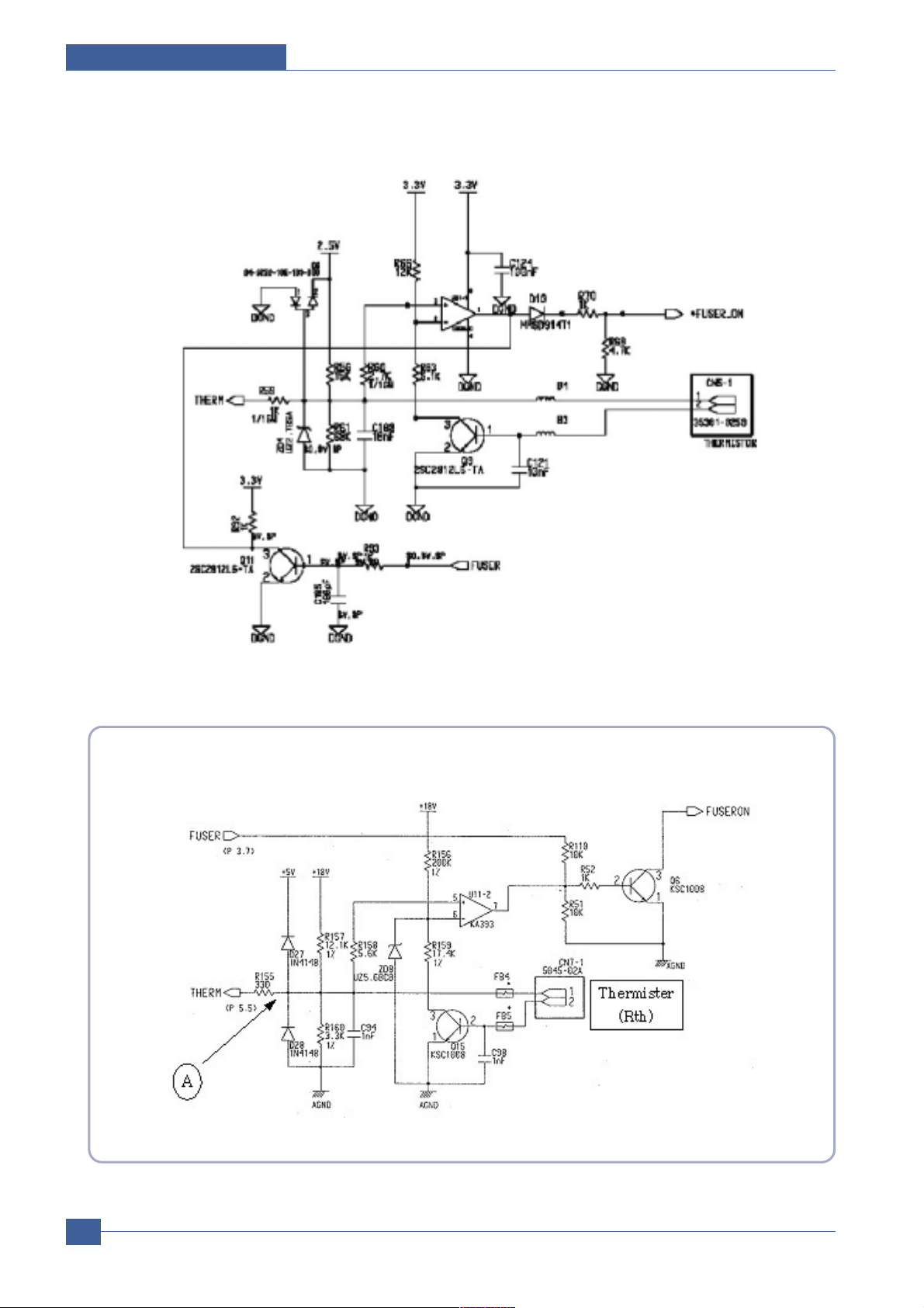
Explanation about the condition of Normal Operation
If the fuser (P3.7) port becomes high, the Q6 is activated. Aheat lamp starts operating by the activity.
As the temperature of the heat lamp is increased, the resistance value of the thermister is decreased.
Therefore, the electric potential of the circled Abecomes low.
On/Off operation of the Q6 is only controlled by the fuser (P3.7) port because 5(+) of the
U11(Comparator) is always higher than 6 (-) within the normal control temperature rage.
Functions of the Malfunction Protection:
If the fuser port (P3.7) is turned on regardless of controlling due to system malfunction, the temperature of the heat roller goes abnormally high. At this time, the resistance value of the thermister becomes
low.
When the resistance value of the thermister becomes low, the electric potential of the circled Agets low,
and when the temperature goes over the certain temperature, the comparator (U11) gets a low output.
As a result, even though the fuser port is abnormally activated, it is disable to be over the regular temperature. For maintaining a regular temperature, a protect circuit consists in it (This protection is set up
to start operating at the rage between 205°~210°)
12.1.2 PWM Controller
Function Description
PWM TIMER consists of each sub block which has various functions. The sub block is divided based on
this block diagram. The entire diagram of the PWMTIMER is organized as below.
PWM TIMER OPERATION is figured out if calculating PHCLK by the value selected by the register setting
and the divider. PHCLK is created by count block at the PWM TIMER
Page 4

Samsung Electronics
Service Manual
Circuit Description
12-4
12.1.3 Motor Driver
A motor drive circuit is decided when selecting a driver IC. (Supplied by vendor) ML1610 uses the motor driver IC of
AN44060. However, the sensing resistance Rs value and the Vreference resistance value are variable according to
the motor drive current value.
12.1.4 LSU Controller
The laser scanning unit controller (LSUC) of Jupiter4E is a block for interface between PVC block and LSU.
LSUC sends the video data received from PVC and the laser diode turn On/Off signal created by inner 21 bit counter
to the laser diode of LSU. LSU creates the horizontal sync signal (nHSYNC) by sensing the inputted diode turn on/off
signal with the attached sensor. nHSYNC is inputted to PVC and LSUC as a signal that informs the beginning of one
line. Also, LSU makes the activity of nLREADY signal (ready to print) low when the polygon motor becomes regularly rotating. LSU can recognize the regular rotation status of the polygon motor by reading nLREADYFlag bit in SFR.
Once the polygon motor regularly rotates, it sends the page sync signal (nPSync) to PVC by writing ‘1’at LSUCON[5]
in LSUC, and PVC starts operating for one page printing. After that, every time nHSYNC signal is created, PVC senses the signal and outputs the video data (PVC_VDO) to LSUC. At this time, LSUC creates the video window (Printing
area) and masks it on the video data sent by PVC. LSUC sends the completed video data (LSU_VDO) to the laser
diode in LSU.
Also, LSUC supplies LSU_CLK, created by counting the system clock with the operation clock source of LSU, for the
use of substitution for oscillator. The SFR is set up in IsuSfr block by receiving the bus control signal from APB bus,
and the settled register values are redelivered to IsuCon block. IsuCon block creates a signal for controlling the laser
diode of LSU and outputs it to a pad. The digital filter module is a digital filter to provide against the noise loaded in
nHSYNC and nLREADY signal which directly get into the chip. It is three layer filter, and the delay time is 3*System
Clock Time.
The interface between PVC and LSUC is shown in the picture.
LSUC
nHSYNC
nHSYNC
LSU_VDO
PVC_VDO
nPSync
nFSYNC
nFSYNC
nLSYNC
VDO
PVC
PVC_TEST_EN
PVC_T EST_EN
1
0
0
1
LSU_VDO
Page 5

Circuit Description
Samsung Electronics
Service Manual
12-5
lsuSfr
PSEL
PENABLE
PADDR[4:0]
PWDATA[31:0]
nLREADY
DigiFilter
nHSYNC_FO
DigiFilter
lsuCon
lsuControl[8:0]
windowOnTime[20:0]
windowOffTime[20:0]
ldOffTime[20:0]
ldOnTime[20:0]
patternDuty[9:0]
lsuClkDuty[18:0]
flagClear
LSU_VDO
LSU_CLK
nPSync
nLREADYFlag
nHSYNC
nLREADY_FO
LS UC
DAC
PD
THER
THV
DAC_OUT
PI
Control
Block
PRDATA[31:0]
PWRITE
APB
BRIDGE
APCCON[11:0]
apcOnTime[20:0]
apcOffTime[20:0]
SHOffTime[20:0]
SHOnTime[20:0]
ENGIN
ADC
E
Pmax[9:0]
Pmin[9:0]
Ka[14:0]
REF[24:0]
Kp[15:0]
Ki[4:0]
Ky
YMAXH[8:0]
YMAXL[31:0]
YMINH[8: 0]
YMINL[31:0]
YINITH[8:0]
YINITL[31:0]
KU[5:0]
U_VALUE[25:0]
SEH[4:0]
SEL[4:0]
L_VALUE[9:0]
HCLR[20:0]
PVC
ADO_2[9:0]
ap
CKIN.
ADC_EN
SEL[1:0]
cOn
ADC
Contro ller
Page 6

Samsung Electronics
Service Manual
Circuit Description
12-6
The main signals used in LSU Controller are shown in the table.
12.1.5 ADC Controller
Jupiter4E ADC Controller has 3 analog input channels.
It automatically converts the 3 channels in turns with 10 bit 500KSPS adc1275x_pc, and also it makes the conversion
on the desired time by manually controlling STC of the register. After finishing the conversion, it makes the interruption to be pending. When AD conversion of 3 rd channel ends for the PI Control of LSU, it sends the 10bit digital data
converted with the latch short pulse signal to LSUC.
Name Direction Description
PVC-VDO I The video data output from PVC.
nLREADY I Its activity becomes low as the polygon motor of LSU gets the regular speed.
nHSYNC I It informs the beginning of one line. It is the same as nLSYNC of PVC.
nPSync 0 It is inputted to nFSync of PVC.
LSU_VDO 0 The completed video data output by masking video window on PVC_VOD.
first field second field
nHSYNC
window On
ldOn
window OnTim e
window Off Time
ldOnTime
ldOffT ime
count er start
testPattern
patternstart
PVC_ VDO
Laser Diode & Window On/Off Time
 Loading...