

Page 1
5. Special Circuit Descriptions
5-1 CD
5-1-1 RF Amp (KA9220) : WIC01
5-1-2 Focus Error Amp (KA9220) : WIC01
5-1-3 Focus Servo System (KA9220) : WIC01
74
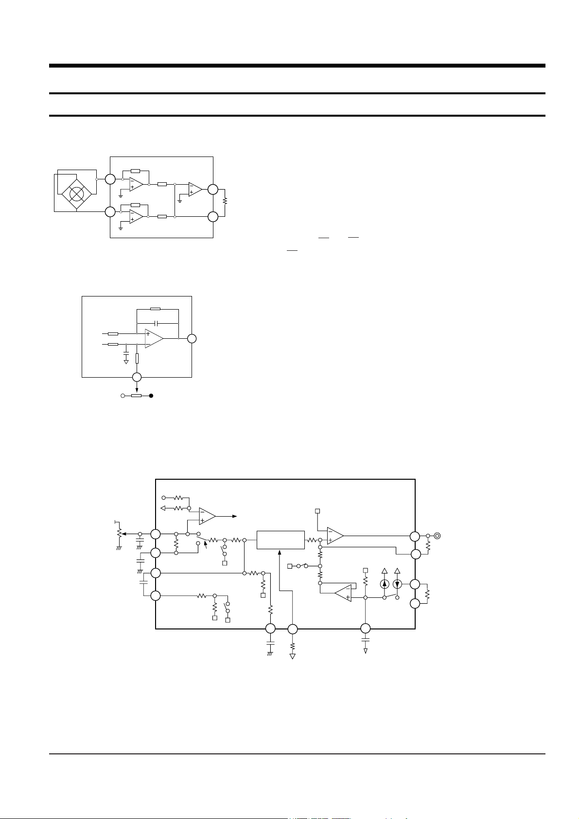
Photo Detector
B
CA
D
PD1
PD2
58K
RF I-V AMP(1)
58K
10K
R2
RF I-V AMP(2)
V2
R1
10K
RF SUMMING
V1 AMP
RFO
RF
66
67
R3
75
RF I-V Amp(I-1) and RF I-V Amp (I-2) are converted to voltage (via
internal resistance of 58k½) from the current of PD1 (A+C) and
PD2 (B+D):
These voltages are added by the RF summing amplifier.
The signal (A+B+C+D) is applied to RFO (No.2 terminal)
RF output voltage is calculated as follows :
FOCUS ERROR Amp AMPLIFIES the difference
between RF I-V Amp (1) output (A+C) and RF I-V Amp (2) output (B+D)
These two signals are supplied to (-) and (+) input terminals of the
FOCUS ERROR Amp. The FOCUS ERROR signal resulting from this
difference voltage is applied to FE (Terminal No. 57).
The FE output voltage of this low frequency component varies according
to {(A+C) - (B+D)}.
VFE is calculated as follows:
VFE=(R2/R1) X (V2-V1) = 5.4(V2-V1)
This FOCUS ERROR voltage is sent to FOCUS SERVO.
When FS3 is ON, high-frequency gain decreases (time constant is set by pin17, pin19, and capacitor connected to
internal resistance). The capacitor between pin18 and GND sets the time constant to pass low freqencies in PLAY
mode.
The maximum frequency of focus phase compensation is inversely proportional to the resistance connected to pin 7.
Focus search peak is about 1.1 Vp-p, and is inversely proportional to the resistance connected to pins 22,23
(if this resistance changes, the peak of track jump and sled kick change). The inversion input of FZC comparator is set
to 5.7% of the difference between Vcc and VC (pin69) {(5.7% x (Vcc-Vc)}.
Note : If the resistance connected to pin 7 changes, the phase compensation peak of focus,tracking,sled servos change.
At the same time, Ôop-ampÕ dynamic range and offset voltage also change.
VRF = -R3 x (iPD1 + iPD2)
= -R3 x (V1/R1 + V2/R2)
= -R3 x ( + )
= x (V1 + V2)
R3
10K
V1
10K
V2
10K
57
63
R2
174K
C1 25P
FE
FOCUS
ERROR
AMP
164K
FE Bias
GNDVcc
20K
32K
C2 25P
-(A+C)
-(B+D)
R1
V1 32K
3.6K
20
21
47
48
60K
FZC
0.0022
20K
0.1UF
0.1UF
FDFCT
HFGD
EFR
FE2
470K
DFCT
FS4
20K 48K
58
60
62
46K
580K FS3
FSW
470K
130K
0.1UF
27
40K
6
PFSET
FS2
PHASE
COMPENSATION
92K
40K
10K
3
4.7UF
FSCH
FS1
50K
5.5U 11U
VREG
180K
ISET
FCE
120K
FOCUS
COIL
FSEO
61
Samsung Electronics 5-1
Page 2
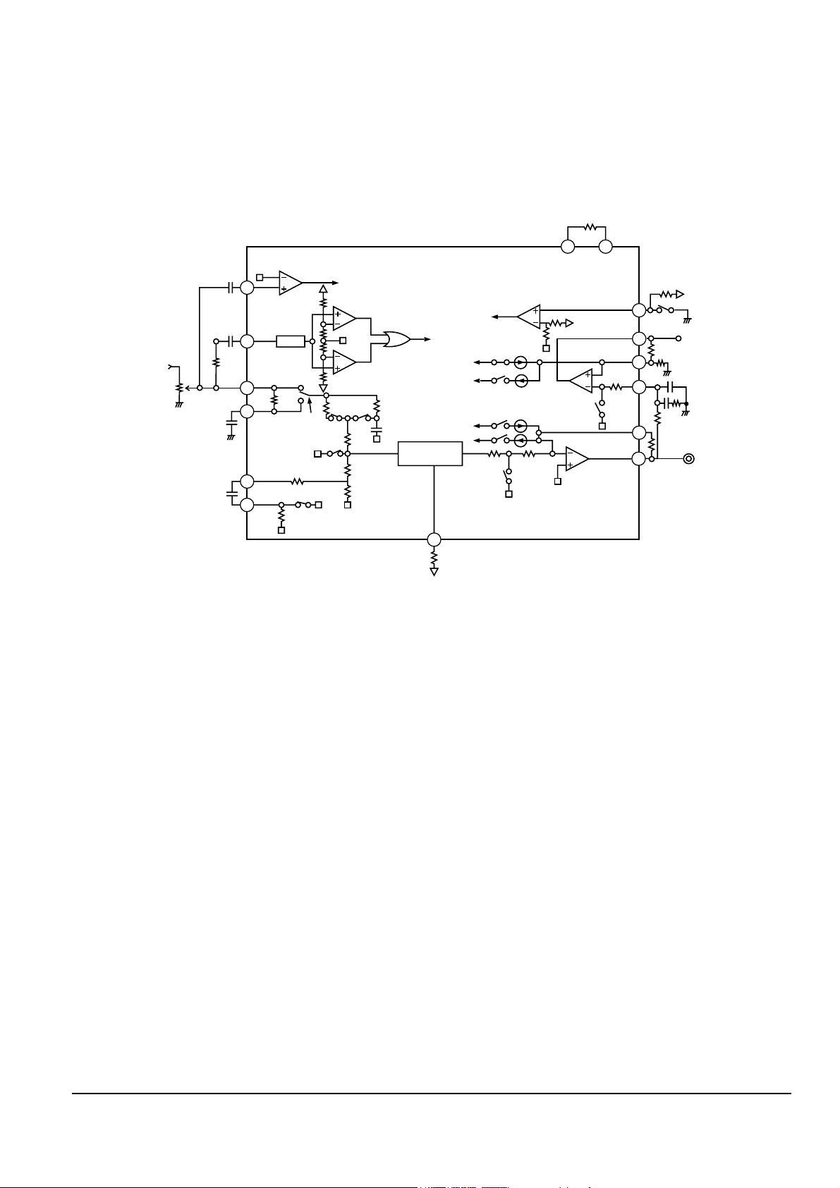
5-1-4 Tracking Sled Servo System (KA9220) : WIC01
The capacitor between pins 15 and 16 attenuates high frequencies when TG2 is off. The maximum frequency of
tracking phase compensation is inversely proportional to the resistance connected to pin 7 (about 1.2kHz at 470k).
The tracking jump (FWD and REV) is determined when TM3 and TM4 are ON, and the peak voltage induced from
tracking coil is decided by both TM3 and TM4 current values and feedback resistance of pin 47.
Tracking jump max voltage = TM3 (TM4) current x feedback reisistance.
FWD or REV sled kick occurs when TM5 or TM6 is ON, and the peak voltage added to sled motor is decided by
TM5 or TM6 current and the feedbadk resistance of pin 41.
Sled jump max voltage= TM5 (TM6) current x feedback resistance
Each SW current is decided by the resistance connected to pin 22 and 23.
When the resistance is about 150½,
TM3 or TM4 = 11µA,
TM5 or TM6 = 22µA,
This current is inversely proportional to the resistor, variable within a range of 5 to 40µA for TM3.
STOP is the ON/OFF detection signal for the limit SW (or the sled motorÕs innermost cirumference).
22 23
40
41
39
47
48
7
15
16
54
52
50
51
0.022UF
TZC
0.047UF
150K
BPF
1K
1K
TZC
100K
ATC
20K
TE 1
TE2
470K
100K
ATS
TDFC1
0.1UF
680K
66PF
10K
DFCT
0.1UF
RTG
20K
TGSW
470K
TG2
82K
110K
PHASE
COMPENSATION
S STOP
1K
100K
S STOP
SLED
SLEI
SLEN
10K
56K
100K
ISET VREG
180K
SLED
DRIVER
120K
100K
TKEO
TKEI
TM2
TM6
TM5
TM4
5.5U
TM3
5.5U
10K
90K
TM7
PFSET
470K
8
TRACKING
COIL
Special Circuit Descriptions
5-2 Samsung Electronics
 Loading...