

Page 1
10. Flow Chart of Troubleshooting
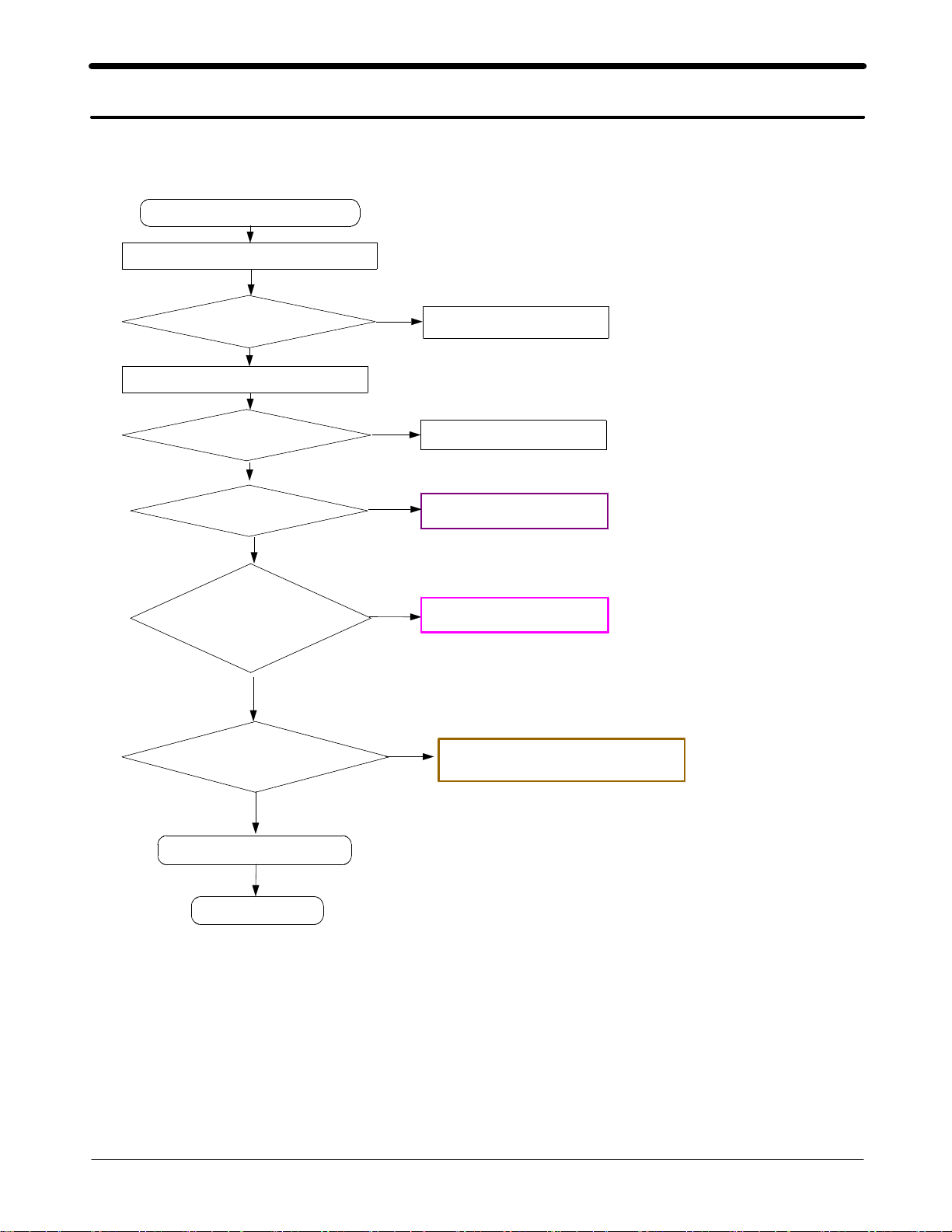
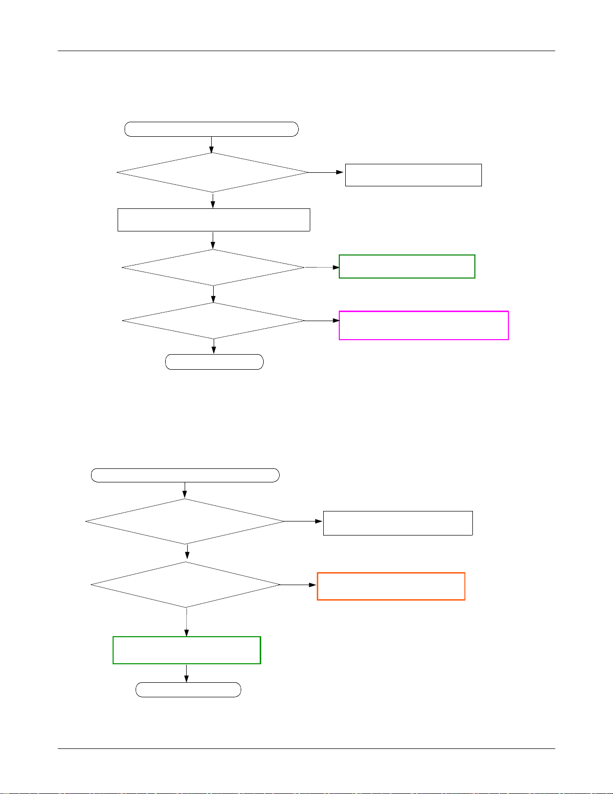
10-1-1.
Power ON
Power On' does not work
'
Check the current consumption
Yes
Current consumption
Check the Vbat Voltage
Voltage
#3
Pin
mA
>= 100
Yes
>=3.3V
Yes
of D400 is high?
Yes
No
No
Download again
Charge the Battery
No
Check D400
Check the PMIC output
voltage
C421,C422,C423,C417,
(
C424,C427)
Yes
Check Pin#3 of TCX200
is
MHz?
19.2
Yes
Check the initial operation
END
No
No
Check PMIC400
Check the clock generation circuit
relatedtoTCX200
(
)
10-1
SAMSUNG Proprietary-Contents may change without notice
This Document can not be used without Samsung's authorization
Page 2
Flow Chart of Troubleshooting
C
C
3
3
0
0
3
C350
R315
C351
R204
6
D
3
0
1
C235
C232
C237C245
T
C
X
2
0
0
D
3
0
0
C
2
3
4
C123
C101
C316
C
3
2
7
E
K
A
W
_
T
S
O
H
_
T
P
T
S
R
_
T
B
_
P
T
TP_BT_RTS
L
T
C
_
G
E
R
V
_
T
B
_
P
T
T
P
_
B
T
_
C
T
S
TP_PCM_SYNC
N
I
D
_
M
C
P
_
P
T
C124
C
C
C
D
4
0
0
4
2
3
3
3
0
C
4
1
3
R407
C
4
1
9
L
1
0
0
C
4
0
2
C104
C
4
2
2
2
2
9
C412
C423
0
0
C421
R400
C414
C416
R401
R
4
0
3
C
4
0
6
4
C
I
M
P
C
C
4
C
4
0
7
4
0
1
9
1
BOTHHOLE706
T
P
_
P
C
M
_
TP_BT_WAKE
0
0
1
D
O
U
T
TP_PCM_CLK
T
B
U
C115
L
F
B
2
1
C
4
1
0
C
TP_VREG_GP2
4
2
0
2
G
4
5
S
C
G
8
4
A
1
0
6
6
8
C
C
4
4
0
2
0
7
T
P
_
B
T
_
E
N
C108
C
1
1
9
R109
C127
C102
C100
C
1
F
1
3
1
0
4
C109
C
4
R
3
4
4
0
6
C428
C
C
4
4
0
0
5
4
C435
R408
BOTHHOLE701
R
1
0
3
MOT700
L
1
0
2
C
4
0
3
A
N
T
3
10-2
SAMSUNG Proprietary-Contents may change without notice
This Document can not be used without Samsung's authorization
Page 3

PMIC Part>
<
PM IC
Flow Chart of Troubleshooting
VBATT
VBATT
3
4
0
0
4
4
C
C
1005
VBUS OVP
VBUS_OUT
4
3
4
C
C406
C407
C408
C405
A7
VF
B7
K3
VF_MSM
TP_AMUX_OUT
SIM_RST
SIM_CLK
R404
L3
L1
L2
D7
H7
D6
H6
D5
H5
SIM_IO
K2
JIG_ON
B4
D4
H8
C11
E10
D10
B5
B6
A5
A6
D8
E4
E11
H10
C430
B10
F11
G4
J1
J2
H2
F4
F2
H4
H1
C411
C410
C412
C409
C413
6
0
4
R
VBATT
TCXO_EN
BUFF_TCXO
BT_TCXO
(Separate from RF line)
USB_DAT_MSM
USB_D_M
USB_D_P
(Same line length & separate from RF line)
USB_OE_MSM
USB_SEO_MSM
(Separate from strong data line)
REF_OUT
BT_EN
TCXO
MSM_SIM_RST
MSM_SIM_CLK
MSM_SIM_IO
C414
R400
MPP1|AMUX_IN1
MPP2|AMUX_IN2
AMUX_OUT
MPP3|VIB_DRV_N
MPP4|LCD_DRV_N
KPD_DRV_N
MPP5|RUIM_M_RST
MPP6|RUIM_RST
MPP9|RUIM_M_CLK
MPP10|RUIM_CLK
MPP11|RUIM_M_IO
MPP12|RUIM_IO
MPP7|CBLPWR_N
MPP8|REF_OUT
OPT_1
OPT_2
REF_BYP
REF_GND
REF_ISET
SPKR_IN_M
SPKR_IN_P
SPKR_OUT_M
SPKR_OUT_P
TCXO_EN_1
TCXO_EN_2
TCXO_IN
TCXO_OUT_1
TCXO_OUT_2
TCXO_OUT_RF
USB_DAT
USB_D_M
USB_D_P
USB_ID
USB_OE_N
USB_OVP_G
USB_SE0
USB_VBUS
D
N
G
5
E
0
1
1
1
3
2
9
4
1
5
7
1
1
1
1
L
E
L
F
B
B
B
A
G
K
H
A
3
F
V
P
C
R
N
N
T
A
B
V
D
N
G
6
E
V
M
M
I
I
2
5
5
R
K
A
G
S
M
A
S
_
U
_
_
L
_
P
S
M
_
R
M
G
D
D
W
S
_
W
M
D
_
_
E
_
D
S
D
_
_
D
VREG_GP1
D
D
D
R
D
V
V
V
D
D
D
V
D
D
V
D
D
V
VREG_GP2
D
V
V
V
V
V
VREG_GP3
VREG_MMC
VREG_MSMA
VREG_MSME
VREG_MSMP
VREG_MSMC
VSW_MSMC
VREG_RFRX1
VREG_RFRX2
VREG_RFTX
VREG_RFUBM
VREG_RUIM
VREG_S2
PMIC400
VREG_S3
VSW_S2
VSW_S3
VREG_TCXO
VREG_USB
VREG_WLAN
XTAL_IN
XTAL_OUT
SBDT|SSBI
BAT_FET_N
CHG_CTL_N
HSET_BIAS
KPD_PWR_N
MSM_INT_N
PON_RESET_N
PS_HOLD
SLEEP_CLK
D
D
D
D
D
D
D
C
N
N
N
N
N
N
N
N
C
C
G
G
G
G
D
N
N
G
G
G
1
7
5
6
7
7
6
5
1
1
2
F
F
F
E
G
G
G
D
V_RF_S2_2.1V
VDD_EAR_2.9V
R402
VREG_MSMP_2.6V
TP_1.8V
C422
S
O
1
P
G
E
2
N
TP_2.6V
C423
BAT400
VREG_MSMC_1.2V
TP_1.2V
C417
VREG_USIM_3.0V
C418
PS_HOLD
BOOT_SW
VREG_SD_2.8V
C433
VREG_MSMA_2.6V
C420
VREG_MSME_1.8V
C421
C432
0
0
4
C402
A3
A2
TP_VREG_GP2
B1
L9
G11
K8
J11
K4
K5
L400
A9
A10
A8
B8
L10
L8
L6
K7
L401
L402
K6
A1
G2
B11
VREG_MSMP_2.6V
VBATT
D1
ISNS_M
D2
ISNS_P
L11
K11
F8
R401
SBCK
G8
E8
R403
SBST
J10
VCOIN
VCHG
VBUS_OUT
E2
C2
C1
K1
L4
C10
G10
F10
K9
C435
R407
C
C415
OSC400
PMIC_SBDT
R408
ON_SW
PM_INT_N
PON_RESET_N
SLEEP_CLK
C431
D400
2
3
1
C419
V_RF_S2_2.1V
V_RF_S3_2.7V
C425
C424
VREG_BT_2.6V
VREG_TCXO_2.8V
C427
C429
C416
C426
C428
10-3
SAMSUNG Proprietary-Contents may change without notice
This Document can not be used without Samsung's authorization
Page 4
Flow Chart of Troubleshooting
10-1-2.
Charging Part
Initial Failure
5.0V @
U400 pin4=High?
Check the Battery&TA
Yes
C601
Yes
Yes
Yes
?
No
if it has some problem, it is to be replaced.)
(
No
Check the CN600
Replace U400
No
Check the U400
JTAG_301
T
P
_
2
.
6
V
END
T
P
_
G
N
W
E
_
_
TP_SDRAM_RAS_N
TP309
M
TP_SDRAM_A[0]
P
I
O
0
4
C447
T
P
_
1
.
8
V
R316
R415
R416
C352
R421 R422
CLIP307
C807
C808
C809
C810
ZD806
C811
C812
A
D
R
S
C650
T
S
P
C
_
M
_
P
T
A
R
D
S
_
P
T
T
P
_
P
S
_
H
O
L
D
TP_RP
U400
C642
3
1
6
U
_
R
D
Y
C745
0
E
_
W
P
T
T
_
D
R
0
3
P
T
P
K
L
C
_
A
M
R
S
D
_
P
T
R420
R
R424
6
0
1
C
6
4
6
C
6
4
4
UME300
U
C
R
R
1
6
8
L
3
0
3
R604
R
6
0
5
L
3
0
0
C342
C341
4
1
8
L301
8
7
1
1
0
5
6
TP_BOOT_SW
TP_JIG_ON
U1411
U605
C
6
0
1
TP_INTB
C600
U805
L710
1
0
8
U
C313C314
C354
C353
U1409
10-4
SAMSUNG Proprietary-Contents may change without notice
This Document can not be used without Samsung's authorization
Page 5
Flow Chart of Troubleshooting
10-1-3.
Sim Part
Insert SIM is displayed on the LCD
"
Yes
Check the SIM connector's
SIM
(
connection to
600)
SIM card
Yes
Check the voltage at pin#1
of SIM
600 >= 3.0V ?
Yes
Is there any signals
pin#2,#3,#4 of SIM
600 ?
No
No
No
Resolder or change SIM
Check the PMIC400
Check the PMIC400
600
Yes
Check the SIM Card
END
VREG_USIM_3.0V
R405
1
VCC
SIM_RST
SIM_CLK
SIM_IO
2
6
1
7
3
4
3
4
1
4
C
U
C
R414
C445
R410
R411
C446
V
C
C
C
R
R
7
7
7
7
7
0
0
0
0
0
6
5
4
3
8
U
C
R
C
1
4
4
4
4
0
1
3
3
5
2
6
7
C438
2
VCC
3
CLK
4
GND
5
0
VPP
6
0
I/O
6
7
NC
8
M
NC
I
9
9
0
8
NC
3
4
3
4
C
SIM CON
5
A
E
H
C
C
C
7
7
7
0
0
0
7
3
2
C
4
4
0
S
10
4
4
C
C
NC
ZD606
C444
U1405
C442C443
ZD605
R413
R412
R817
C441
R409
R
R
R
8
8
8
1
1
1
4
3
2
C
4
3
9
SIM600
10-5
SAMSUNG Proprietary-Contents may change without notice
This Document can not be used without Samsung's authorization
Page 6
Flow Chart of Troubleshooting
10-1-4.
Microphone Part
Microphone does not work
Is the soldering status of
microphone O.K?
Check the reference voltage on MAIN-MIC path
1.8V @
Is microphone ok?
END
Yes
Yes
Yes
R500
Yes
Yes
No
Resoldamicrophone
?
No
No
Check UCP300
Check the path
or replaceamicrophone
around MIC_BIAS circuit
10-1-5.
Receiver Part
There is no sound from the Receiver
Yes
Is the terminal of Receiver
Is there any signals at R713
Check HEA701
RECEIVER/SPEAKER/ear jack FPCB.
O.K
?
and R714
#7, #9
END
Yes
Yes
?
No
Replace the Receiver
No
Check UCP300
Pin and
10-6
SAMSUNG Proprietary-Contents may change without notice
This Document can not be used without Samsung's authorization
Page 7
Flow Chart of Troubleshooting
O
S
C
4
0
C
R
6
6
0
0
6
6
L400 L401L402
CLIP311
Z
D
C516
7
0
1
R505
Z
D
7
R504
0
2
MIC400
MIC_BIAS
R500
C508
R502
MIC1_P
MIC1_N
C509
C511
C515
C517
C502
C503
R506
C
0
4
3
1
C
C
R402
4
4
3
3
C
5
1
3
C502
C513
C516
2
3
R504
MIC1P_F
R505
MIC1N_F
C
6
4
1
2
C
2
4
0
C
6
4
3
1
6
ZD800
C
8
2
6
C
8
2
7
C
8
2
0
C
8
2
1
C819
V2
C
2
3
9
MIC_MAIN
F
7
0
3
A
V
R
L602
C
F
1
4
S
7
0
3
0
Q
0
2
3
0
1
0
0
R
F
7
C746
0
4
C
6
3
3
C
8
U
3
3
C825
Z
D
8
0
1
C
C
C
8
8
8
2
3
2
9
0
8
C
C
C
8
8
8
2
2
2
2
3
4
Z
D
8
0
3
ZD802
C
C
C
R
2
2
2
2
4
2
2
1
2
6
5
1
ZD300
C
R
T
-
4
6
D
1
8
1
3
2
K
R311
0
2
6
0
1
P
R
U
R310
C
6
2
C628
R312
9
C
3
1
8
C
C
3
3
2
2
3
2
C305
C302
C307
C301
C348
R313
R308
C355
C345
R732
C356
C343
C329
T
C
P
_
C331
A
M
3
U
X
4
_
O
U
6
T
R734R736
C333
C
C
C
C
C
R
2
2
2
2
2
2
2
2
4
3
4
1
8
7
8
1
4
0
P
0
0
3
C
U
T
P
R
R
R
R
R
R
R
_
M
3
O
0
D
E
2
3
0
0
R
3
3
5
3
3
3
5
C319
0
0
2
0
0
0
2
3
6
1
1
5
0
0
R314
C320
C
3
0
C316
6
D
D
3
3
C
0
0
3
0
1
2
7
C350
C
3
0
3
TP_1.2V
C
C
C
C
3
3
3
2
1
2
3
4
1
7
2
5
C304
C309
C300
C308
R304
C344
C330
C328
C332
R404
C312
C311
C310
L
3
0
2
BOTHHOLE706
10-7
SAMSUNG Proprietary-Contents may change without notice
This Document can not be used without Samsung's authorization
Page 8

Flow Chart of Troubleshooting
10-1-6.
Speaker Part
There is no sound from the Speaker
Is the terminal of Speaker O.
Is there any signals at
Check HDC703
RECEIVER/SPEAKER/MOTOR FPCB.
Yes
K?
Yes
Is there any signals at
R711 and R712
Yes
L500 and L501
Yes
pin and
#1, #3
Yes
No
Replace the Speaker
No
check the UCP300
No
Check the U501 and circuit around
SPK_N_OUT
SPK_P_OUT
VOICE_OUT_N
VOICE_OUT_P
END
3
0
6
P
L
I
C
C724
R713
R714
R506
C515
C509
8
R502
0
3
P
I
R500 R501
L
C
R
5
0
7
R
5
1
8
R711
R712
R713
R714
D700
D701
C514
C507
C501C503
R
5
1
0
R
5
2
2
CLIP302
1
0
7
D
C519
C523
C524
C534
C533
C505
C
5
R503
3
1
V
V
C
R
R
R
5
1
1
R
5
0
8
7
7
7
2
5
2
0
9
6
R809
9
0
2
3
6
7
7
7
2
2
7
7
R
R
C
C
V
V
C725
C517
C
C
5
5
1
1
1
0
C
C
5
5
0
0
4
8
R515
5
0
2
U
0
4
5
0
2
2
7
7
7
D
C
C
SPK & RECEIVER & 3.5 PI
C
C526
U
HEA701
1
3344
5566
7
9
R733
C
7
VR732
R513
2
3
L703
R516
C
L704
R517
7
2
2
VR731
R514
R715
C527
C
C525
R806
C
5
1
8
10
R735
L709
V
R
7
3
0
U
1
4
0
3
2
L703
2
L704
1005
8
10
1
2
3
3
2
3
7
7
2
2
7
7
R
R
V
V
C
C
3.5PI_EAR_R
3.5PI_EAR_L
JACK_INT_3.5PI
0
5
5
1
7
7
R
R
V
5
3
2
C
7
2
7
5
2
0
1
5
0
R
R
5
5
0
1
9
2
R
R
7
7
1
1
1
2
U
5
0
3
1
78
9
10-8
SAMSUNG Proprietary-Contents may change without notice
This Document can not be used without Samsung's authorization
Page 9

Flow Chart of Troubleshooting
10-1-7.
EARPHONE Part
There is no sound(VOICE)from the Earphone
Is the Headset O.K?
I
Check the reference voltage on Ear-MIC path
1.8V @
Is there any signals at
Check the CN600
R503
Yes
Yes
Yes
R501
Yes
Yes
Yes
No
Change the Headset
?
No
Check UCP300
No
Check the path
around MIC_BIAS circuit
END
MIC_BIAS
R501
C504
C507
MIC2_P EARMIC_P
C510
MIC2_N
C514
C501
C505
R503
MIC_EAR
10-9
SAMSUNG Proprietary-Contents may change without notice
This Document can not be used without Samsung's authorization
Page 10

Flow Chart of Troubleshooting
There is no sound(MUSIC)to the Earphone
Yes
Is the Headset O.K?
I
Yes
Is there any signals at
C523 and C524
Yes
Is there any signals at
R512 and R514
Yes
Check the IFC600
Yes
END
EAR_OUT_R 3.5PI_EAR_R_SW
EAR_OUT_L
VREG_MSMP_2.6V
I2C_AUDIO_SDA
I2C_AUDIO_SCL
No
Change the Headset
No
check the UCP300
No
Check the U501 and circuit around
VBATT
0
2
5
C
9
1
5
C
C533
AUXON
C534
AUXOP
C523
C524
1
0
2
2
5
5
R
R
1
5
B
C
D
D
D
D
V
V
P
D4
D5
RXIN-
OUT-
B4
B5
RXIN+
OUT+
D2
HPRA1INA1
A2
D1
HPL
INA2
U501
C2
A4
INB1
C1N
C1
A5
INB2
C1P
1
B2
NC
BIAS
B3
2
SDA
NC
C3
SCL
D
D
N
S
N
S
G
V
G
P
3
4
3
A
C
D
C526
C527
R509
R512
R513
R514
R516
R517
C525
SPK_N_OUT
SPK_P_OUT
EAR_R
EAR_L
3.5PI_EAR_L_SW
C531
C532
SPK & EAR AMP
3
L
0
6
I
C
P
C724
R713
D700
R714
C725
D701
C517
R506
C
C
C515
5
5
C514
1
1
0
1
C509
C
C
R515
C507
5
5
0
0
4
8
C501C503
R
5
1
0
R
5
2
0
5
U
2
2
CLIP302
R502
R500 R501
R
5
0
7
R
5
1
8
C
5
2
C519
0
C523
1
C524
C534
C533
C505
C
R
5
5
R503
3
0
1
9
V
V
R
C
R
R
7
5
0
R809
7
7
7
1
2
2
1
6
9
R
5
1
1
R
5
0
8
R733
C526
C
7
R513
VR732
2
3
L703
R516
0
5
U
C
L704
R517
7
2
2
R514
VR731
R715
C527
R
C
C525
5
1
2
R
7
1
2
U
5
0
3
R735
5
3
2
L709
V
C
R
7
7
2
3
7
0
R806
U
C
1
5
4
1
0
8
3
10-10
SAMSUNG Proprietary-Contents may change without notice
This Document can not be used without Samsung's authorization
Page 11

Flow Chart of Troubleshooting
10-1-8.
FM RADIO Part
FM Radio does not work
Turn on the Radio.
check the Voltage at
C619(3.0V)
Is there any signal at C801
and C802
Is there any signal at C523
and C524?
Yes
Yes
Yes
No
No
No
Check U606
Resold or replace the UFM100
check the UCP300
Yes
Is there any signal at R513
and R514?
Yes
Check the EAR/SPEAKER Path.
No
check the U501
10-11
SAMSUNG Proprietary-Contents may change without notice
This Document can not be used without Samsung's authorization
Page 12

Flow Chart of Troubleshooting
FM_ANT
I2C_FM_RADIO_SCL
I2C_FM_RADIO_SDA
SLEEP_CLK
RADIO_EN
L802
VREG_MSMP_2.6V
R802
VBATT
U606
VDD4VOUT
3
R609
R610
CE
5
C617
V_RADIO
R608
1
2
GND
D
N
G
9
1
6
C
RADIO REGULATOR
R800
20
19
18 17
21
23
22
1
U800
8
3
2
C
O
O
O
N
I
I
I
P
P
P
G
G
G
LOUT
ROUT
K
L
O
I
C
O
D
I
R
S
V
10
9
R803
RADIO_RST
D
C
C
N
N
N
G
1
NC
C800
2
FMIP
3
RFGND
4
GND
5
_RST
6
_SEN
K
L
C
S
7
RADIO_RST
C618
VREG_MSMP_2.6V
R801
16
VA
15
GND
14
13
12
GND
11
VD
C803
V_RADIO
0
1
0
0
8
8
L
L
C801
C802
C804
C805
RADIO_INT
AFL
AFR
- FM RADIO -
10-12
SAMSUNG Proprietary-Contents may change without notice
This Document can not be used without Samsung's authorization
Page 13

Flow Chart of Troubleshooting
10-2-1.
EGSM
900
RX
NORMAL CONDITION
catch the channel?
YES
PAM
pin
PAM
pin#5
CHECK
100
100
≥
dBm
CHECK
dBm
-65
YES
#8≥-65
F101 CHECK?
?
YES
?
NO
NO
NO
NO
CHECK
ANT contact
PAM
re-solder or change
re-solder or change
re-solder or change
100,
PAM
F101
RFS
100
100
Band:EGSM
CELL POWER
Channel
?
:-50
:62
dBm
Ch
YES
TCXO CLOCK CHECK?
MHz@C229
19.2
YES
U200 Check?
YES
UCP300 CHECK!!
NO
NO
TCX200, C21290
re-solder or change
U200
change or re-solder
10-13
SAMSUNG Proprietary-Contents may change without notice
This Document can not be used without Samsung's authorization
Page 14

Flow Chart of Troubleshooting
10-2-2.
DCS
1800
RX
NORMAL CONDITION
catch the channel?
YES
PAM
pin
PAM
pin#
CHECK
100
6≥
100
CHECK
dBm
-65
dBm
YES
YES
#8≥-65
F102 CHECK?
?
YES
?
NO
NO
NO
NO
CHECK
ANT contact
PAM
re-solder or change
re-solder or change
re-solder or change
100,
PAM
F102
RFS
100
100
Band:DCS
CELL POWER
Channel
?
: 698
:-50
Ch
dBm
TCXO CLOCK CHECK?
MHz@C2290
19.2
YES
U200 Check?
YES
UCP300 CHECK!!
NO
NO
TCX200, C220
re-solder or change
U200
change or re-solder
10-14
SAMSUNG Proprietary-Contents may change without notice
This Document can not be used without Samsung's authorization
Page 15

Flow Chart of Troubleshooting
10-2-3. PCS1900
RX
NORMAL CONDITION
catch the channel?
YES
PAM
pin
PAM
pin#7
CHECK
100
100
≥
dBm
CHECK
dBm
-65
YES
YES
#8≥-65
F103 CHECK?
?
YES
?
NO
NO
NO
NO
CHECK
ANT contact
PAM
re-solder or change
re-solder or change
re-solder or change
100,
PAM
F103
RFS
100
100
Band:PCS
CELL POWER
Channel
?
: 661
:-50
Ch
dBm
TCXO CLOCK CHECK?
MHz@C229
19.2
YES
U200 Check?
YES
UCP300 CHECK!!
NO
NO
TCX200, C229
re-solder or change
U200
change or re-solder
10-15
SAMSUNG Proprietary-Contents may change without notice
This Document can not be used without Samsung's authorization
Page 16

Flow Chart of Troubleshooting
10-2-4.
WCDMA2100 RX
NORMAL CONDITION
catch the channel?
YES
PAM
pin
PAM
pin#10
DUP200 CHECK?
100
#8≥-65
100
-65
≥
CHECK
dBm
CHECK
dBm
YES
YES
?
YES
?
NO
NO
NO
NO
CHECK
ANT contact
PAM
re-solder or change
re-solder or change
re-solder or change
100,
PAM
DUP200
RFS
100
100
Band:WCDMA
CELL POWER
DL Channel
UL Channel
?
:-50
: 10700
: 9750
dBm
Ch
Ch
U200 Check?
YES
F200 Check?
YES
TCXO CLOCK CHECK?
MHz@C229
19.2
YES
UCP300 CHECK!!
NO
NO
NO
U200
change or re-solder
F200
re-solder or change
TCX200, C229
re-solder or change
10-16
SAMSUNG Proprietary-Contents may change without notice
This Document can not be used without Samsung's authorization
Page 17

Flow Chart of Troubleshooting
10-2-5.
EGSM
900
TX
TX Power is too Low!!
TCXO CLOCK CHECK?
MHz@C229
19.2
Check the Power
Pin#55 of U200
Check the Attenuation
Check the Power@Pin#8
of PAM100?
Circuit
YES
?
YES
YES
Band:GSM
CELL POWER
Tx Power : 5Level
Channel : 62ch
NO
@
?
NO
NO
NO
TCX200, C229
re-solder or change
CHECK
U200 and C223
CHECK R111, R113,
R114
PAM100
re-solder or change
:-50
dBm
YES
Check RFS100?
YES
Antenna
re-solder or change
NO
RFS100
change or re-solder
10-17
SAMSUNG Proprietary-Contents may change without notice
This Document can not be used without Samsung's authorization
Page 18

Flow Chart of Troubleshooting
10-2-6.
DCS1800/PCS1900 TX
TX Power is too Low!!
TCXO CLOCK CHECK?
MHz@C229
19.2
Check the Power
Pin#56 of U200
Check the Attenuation
Circuit
Check the Power@Pin#8
of PAM100?
YES
?
YES
YES
Band:DCS/PCS
CELL POWER
Tx Power : 0Level
Channel : 660ch
NO
@
?
NO
NO
NO
TCX200, C229
re-solder or change
CHECK
U200 and C222
CHECK R106, R107,
R108
PAM100
re-solder or change
:-50
dBm
YES
Check RFS100?
YES
Antenna
re-solder or change
NO
RFS100
change or re-solder
10-18
SAMSUNG Proprietary-Contents may change without notice
This Document can not be used without Samsung's authorization
Page 19

Flow Chart of Troubleshooting
10-2-7.
WCDMA2100 TX
TX Power is too Low!!
TCXO CLOCK CHECK?
MHz@C229
19.2
YES
Check the Power
Pin#59 of U200
Check F201
Check PAM200
@
?
YES
?
YES
?
NO
NO
NO
NO
TCX200, C229
re-solder or change
CHECK
U200 and L205
F201
re-solder or change
PAM200
re-solder or change
Band:WCDMA
CELL POWER
DL Channel
UL Channel
Target Power : 24dBm
:-50
: 10700
: 9750
dBm
Ch
Ch
YES
Check DUP200
Check the Power@Pin#8
of PAM100?
Check RFS100?
Antenna
re-solder or change
?
YES
YES
YES
NO
NO
NO
DUP200
re-solder or change
PAM100
re-solder or change
RFS100
change or re-solder
10-19
SAMSUNG Proprietary-Contents may change without notice
This Document can not be used without Samsung's authorization
Page 20

B
O
T
H
H
O
L
E
7
0
3
C251
BOTHHOLE700
C
2
5
8
C
2
6
0
C
2
5
9
0
0
2
F
R
2
0
8
C
2
5
6
C
C
R
2
2
2
5
5
0
5
7
6
C264
C267
C266
C265
C263
C268
R
C
2
2
0
6
7
1
L
C254
2
0
7
C250
Z
H
C252
C
G
4
B
0
0
4
1
G
C253
2
B
K
6
F
R
A
F
R209
R
L
2
2
0
0
6
5
C
C
2
2
4
4
8
7
RFS100
Flow Chart of Troubleshooting
C
2
4
3
C
2
6
2
C
C
L
2
2
2
0
4
4
3
9
6
C206
C
2
0
5
L
C107
C806
1
0
1
C103
R805
L111L112
C106
TP_ANTTP_GND
C
C
C
2
4
0
C
C
C
R
C
2
2
3
2
9
6
0
L109
C
1
3
4
3
0
1
F
C
L
1
1
1
3
0
1
C
C
C
2
2
5
0
C
1
3
2
1
5
B
U
5
M
0
6
9
1
4
1
F
S
L
1
0
8
R
2
2
2
2
2
2
2
2
4
4
4
1
3
2
2
1
C
4
2
1
1
8
8
7
0
2
2
4
R203
C221
C
2
1
3
C
2
1
2
C
C
C
C
2
2
2
2
1
2
1
1
7
0
6
9
R107 R108
C222
2
U
L107
C
C
1
1
3
2
0
6
F
A
D
T
2
2
4
0
8
1
1
H
F
C
F
E
C
C
1
1
2
2
5
0
R106
C223
R113
C215
R111
R114
C218
C
C
2
2
3
3
1
0
R
C
3
3
C
0
3
1
L103
L105
1
7
5
0
C
C
C
C
1
1
1
1
1
1
2
2
4
1
2
1
T
C
H
3
3
3
1
5
0
B
4
0
U
1
5
0
1
M
0
1
0
0
8
4
8
1
1
0
C
C
C
R
9
-
F
F
4
1
1
1
1
1
B
F
3
2
2
1
S
5
9
8
0
C
L
L
1
1
1
0
0
1
4
6
2
C
1
1
8
P
C
C
1
1
A
1
1
7
6
M
C
R
1
1
3
1
1
3
2
0
0
DCS1800_PCS1900_TX
GSM_TX
R106
R107
R108
R111
R113
R114
VBATT
C116
UMTS_2100_ANT
GSM_ANT_SEL1_N
GSM_ANT_SEL0_N
C117 C118
C128
C129
GSM_PA_PWR_CTRL
GSM_ANT_SEL2_N
<2.5G RF & ANT>
C103
R805
6
0
8
C
C107
8
26
VBATT
10
WCDMA1
21
DCS|PCS_IN
23
GSM_IN
27
BS2
28
BS1
29 GND
D
N
G
9
4
T
N
RX4
A
5
RX3
6
RX2
7
RX1
PAM100
2
MODE
3
RSVD
1
_TXEN
25
VAPC
D
D
D
D
D
D
D
D
D
D
D
D
N
N
N
N
N
N
N
N
N
N
N
N
G
G
G
G
G
G
G
G
G
G
G
G
9
8
7
6
5
4
3
1
0
2
4
2
1
1
1
1
1
1
1
1
2
2
2
1
R110
R112
C133
C135
RFS100
G
C
A
G
1
4
2
3
L111
TP_ANT
ANT_JTAG
TP_GND
C106
L112
L101
C110
F100
C112
1
IN
G5G
L104
2
F101
C120
1
IN
G2G
L106
F102
C125
1
IN
G25G
L108
F103
C131
1
IN
2G5
L110
C111
3
OUT
4
OUT
C114
C121
3
OUT
4
OUT
C122
5
C126
3
OUT
4
OUT
C130
C132
3
OUT
4
OUT
G
C134
GSM_850_RX_N
L103
GSM_850_RX_P
GSM_900_RX_N
L105
GSM_900_RX_P
DCS_RX_N
L107
DCS_RX_P
PCS_RX_N
L109
PCS_RX_P
UMTS_2100_TX
VBATT
9
6
2
C201
C
F201
C204
4
1
OUT
IN
G2G3G
5
PA_RANGE1 UMTS_2100_RX
L204
PA_RANGE0
PA_ON
C211
VCC1 VCC2
1
RFIN
2
VMODE1
3
VMODE0
4
EN
11
1213
C209
C210
V_RF_S3_2.7V
C243
C240
PAM200
D
D
N
N
G
G
14
V_RF_S2_2.1V
D
D
N
N
G
G
15
C224
C244
V_RF_S2_2.1V
C202 C203
10
GND
9
RFOUT
8
GND
7
CPL
65
D
D
D
D
N
N
N
N
C
G
G
G
G
N
1617
19
18
R201
TX_I_N
TX_I_P
TX_Q_N
TX_Q_P
DAC_REF
R210
0603
R211
0603
C227
C228
RTR6280_TCXO
C239
C242
C241
R206
R207
C256
SSBDT_RTR
C255
PWR_DET
R200
R202
C212
C213
C221
close to pin68
R203
C225
C226
C238
RX_Q_P
RX_Q_N
C257
0603
6
7
8
1
0
9
6
6
6
7
7
6
ground
F
S
C
ground
C
G
E
A
N
N
U
I
R
L
I
B
S
_
1
R
_
C
_
VDDA2
D
A
X
2
N
T
D
TCXO
G
3
VDDA1
4
VDDA1
5
VTUNE1
6
VDDA1
7
VDDA2
8
NC
9
NC
10
VDDA1
11
PRX_QP
12
PRX_QN
13
RX_I_N
PRX_IN
14
RX_I_P
PRX_IP
15
NC
16
NC
17
NC
2
T
A
D
D
C
C
B
D
N
N
S
V
8
9
0
1
2
1
1
2
2
2
3
0
C261
C262
C259
C260
C258
6
0
V_RF_S3_2.7V
C264
C265
DUP200
L202
C207
C208
5
4
3
2
1
5
4
7
2
6
3
0
8
9
6
6
6
6
6
5
5
5
5
5
5
6
5
5
1
2
3
1
2
2
2
2
1
2
P
P
N
N
N
I
I
I
T
T
T
T
T
A
A
A
A
A
Q
Q
_
_
_
U
U
U
U
U
_
D
D
D
D
D
_
T
X
X
O
O
O
X
O
O
X
D
D
D
D
D
T
T
E
_
_
_
_
_
T
T
V
V
V
V
V
D
GCELL_INN
F
F
F
F
F
P
R
R
R
R
R
GCELL_INP
_
_
_
_
_
B
B
B
B
B
EGSM_INN
L
L
H
H
H
EGSM_INP
DCS_INN
DCS_INP
GPCS_INN
U200
GPCS_INP
T
WPRXSE1
U
O
P
M
_
N
N
P
M
P
M
2
I
I
WPRXSE2
B
_
_
B
E
B
B
2
X
X
WPRXSE1_OUT
H
L
L
H
S
2
2
1
E
N
X
X
X
X
X
M
M
A
A
A
M
N
O
_
_
R
R
R
R
R
D
D
D
D
_
U
P
P
P
P
B
B
P
F
D
D
D
D
T
W
V
W
W
W
R
V
W
W
V
W
V
V
0
5
1
2
6
7
8
9
3
3
4
4
3
2
3
3
2
2
2
2
3
2
2
3
C253
C252
N
O
_
X
T
_
N
O
_
F
R
P
N
_
_
X
X
R
R
_
_
0
0
0
0
1
1
2
2
VREG_MSMP_2.6V
_
_
C263
S
S
T
T
M
M
U
U
3
3
0
0
6
6
0
0
C268
C266
C267
2
ANT
G
G3G
1
46G8
L205
C222
C223
51
50
49
48
47
46
45
44
43
NC
42
NC
41
NC
40
NC
39
NC
38
37
NC
36
35
L200
C205
RX57TX
G
G
9
C214
UMTS_2100_TX
DCS1800_PCS1900_TX
GSM_TX
PWR_DET
C236
C246
UMTS_2100_RX
C249
R209
<RTR6280>
C200
UMTS_2100_ANT
L201
L203
C206
V_RF_S2_2.1V
V_RF_S3_2.7V
V_RF_S2_2.1V
IN
2
F200
C217
C216
C220
C219
UMTS_2100_RX_N
C250
3
L207
OUT
4
OUT
GG
C254
5
UMTS_2100_RX_P
C215
C218
C230
C231
GSM_850_RX_N
GSM_850_RX_P
GSM_900_RX_N
GSM_900_RX_P
DCS_RX_N
DCS_RX_P
PCS_RX_N
PCS_RX_P
C248
C247
5
6
0
0
2
2
L
R
C251
1
8
0
2
R
<3G RF>
10-20
SAMSUNG Proprietary-Contents may change without notice
This Document can not be used without Samsung's authorization
Page 21

Flow Chart of Troubleshooting
10-2-8.
Bluetooth Part
Check the Connection Disable!
Check BT Activation?
YES
Check the Voltage
C101(2.6V), C108(2.6V)
@
YES
Check the Clock
C229
Check BT ANT?
@
YES
NO
Enable BT Function
NO
NO
NO
CHECK PMIC400
CHECK TCX200
BT_ANT
re-solder or change
YES
Exchange BT Module
YES
END
10-21
SAMSUNG Proprietary-Contents may change without notice
This Document can not be used without Samsung's authorization
Page 22

PCM_CLK
PCM_DOUT
PCM_SYNC
PCM_DIN
VREG_MSMP_2.6V
C108
UART1_RFR
UART1_CTS
UART1_TX
UART1_RX
nBT_PWDN
TP_PCM_CLK
TP_PCM_DOUT
TP_PCM_DIN
TP_PCM_SYNC
VREG_MSMP_2.6V
TP_BT_VREG_CTL
TP_BT_CTS
TP_BT_RTS
Close to A3
4
2
1
C
C350
R315
C351
R204
VREG_BT_2.6V
2
0
0
0
1
1
C
C
L100
1
2
8
1
7
7
9
9
1
J
J
A
G
B
A
H
G
G
L
F
P
B
C
C
O
O
O
I
L
F
S
L
D
D
D
D
I
D
P
U
D
D
D
D
D
D
D
D
_
D
V
V
V
V
D
V
D
O
V
V
V
D
D
F8
D9
D8
A9
A8
J6
H6
H5
C8
C9
B9
B8
A3
A2
B3
C
2
2
9
D
4
0
0
C412
V
PCM_CLK|SCK
PCM_INE8BT_PRIORITY|TX_REZ|GPIO3
PCM_OUT
WLAN_ACTIVITY|TX_CONFIRM|GPIO_2
PCM_SYNC
XTAL_PD|GPIO5TX_PU_TDD
SCL|TX_PU_TDD_N
SDA|TX_PU_TDD
TM0
UBT100
TM1
TM2
UART_CTS_N
UART_RTS_N
(Vpp : 1.2~1.5V)
UART_RXD
UART_TXD
VREG1
VREG2
VREG_CTL
S
S
S
S
S
S
S
S
S
S
S
S
S
S
S
S
S
S
S
S
V
V
V
V
V
V
V
V
V
V
6
2
5
2
2
1
2
4
5
6
F
F
E
E
E
E
D
D
D
C
D
D
3
3
C
0
0
3
0
1
2
7
E
K
A
W
_
C
T
S
O
2
H
_
T
P
3
T
C235
S
R
4
_
T
B
_
P
T
C232
TP_BT_RTS
C237C245
T
C
C123
X
2
C101
0
0
C124
C
C
2
4
L
3
3
1
3
0
0
0
R407
C
4
C
C
C
2
4
4
4
2
1
1
0
3
9
2
C423
0
0
4
C421
C
I
R400
M
P
C414
C416
R401
C
C
4
4
R
C
C
1
0
4
4
4
1
9
0
0
0
3
6
7
2
1
4
1
B
H
A
B
O
F
F
V
C
3
T
R
V
R
D
D
D
D
D
D
D
V
D
V
V
V
BT_WAKE|GPIO_0
HOST_WAKE|GPIO_1
STATUS|GPIO_4
PA_CTL|GPIO6
S
S
S
S
S
S
S
S
V
V
V
V
2
4
5
6
F
F
F
H
BOTHHOLE706
T
P
_
B
T
_
C
T
S
L
T
C
_
G
E
R
TP_PCM_SYNC
V
_
T
B
_
P
T
N
I
D
_
M
TP_BT_WAKE
C
P
_
P
T
0
0
1
T
B
U
C104
C
4
1
0
C
4
2
0
1
0
1
C
C104
4
H
O
X
D
D
V
TP_BT_WAKE
B5
TP_HOST_WAKE
B6
E9
A6
F9
TP_BT_EN
G9
H8
H7
GPIO7
J8
HUSB_DN
J7
HUSB_DP
E1
RFION
C1
RFIOP
J4
XTALN
J5
XTALP
J3
RES
D1
RFTUNE
B4
RST_N
A5
LPOIN
D4
TST1
J2
VCTRIFP
S
C
C
S
V
N
N
3
2
1
H
T
P
_
B
T
T
P
_
_
E
P
C
N
M
_
TP_PCM_CLK
D
O
U
T
C115
L
F
B
2
F
1
2
G
1
4
5
0
C
S
G
4
8
4
A
0
1
6
8
6
R
4
0
6
C428
C
4
0
4
C435
R408
C
C
TP_VREG_GP2
4
4
0
2
0
7
F104
BT_WAKE
HOST_WAKE
BT_EN
C115
C119
R103
TP_BT_RST
C123
7
2
9
1
0
1
C
R
BT_TCXO
BT_RESET
SLEEP_CLK
IN4OUT
GND
1
2
GND
3
- Bluetooth -
C108
C
R
1
1
0
1
3
9
R109
C127
MOT700
C102
C100
C
L
1
1
0
1
2
3
C109
C
4
3
4
C
4
C
0
4
3
0
5
BOTHHOLE701
A
N
T
3
Flow Chart of Troubleshooting
C109
L102
C113
10-22
SAMSUNG Proprietary-Contents may change without notice
This Document can not be used without Samsung's authorization
 Loading...