

Samsung M300 Service Manual
GSM TELEPHONE
SGH-M300
GSM TELEPHONE
CONTENTS
Specification
1.
Exploded View and Parts list
2.
Chart of Troubleshooting
3.
Array course control
4.
Block Diagrams
5.
PCB Diagrams
6.
MAIN Electrical Parts List
7.
Reference data
8.
Safety Precautions
9.
Product Function
10.

Specification
1.
GSM/CDMA General Specification
1-1.
GSM TX power class
1-2.
Exploded View and Parts list
2.
Cellular phone Exploded View
2-1.
Cellular phone Parts list
2-2.
Disassembly
2-3.
Assembly
2-4.
LCD KIT Assembly
2-5.
ChartofTroubleshooting
3.
Baseband
3-1.
...............................................................................................................2-4
....................................................................................................................2-8
..................................................................................................2-10
............................................................................................................3-1
Contents
...........................................................................1-1
...............................................................................................1-2
..................................................................................2-1
............................................................................................2-2
3-1-1.
3-1-2.
3-1-3.
3-1-4.
3-1-5.
3-1-6.
3-1-7.
3-1-8.
3-1-9.
3-2.
3-2-1.
3-2-2.
3-2-3.
3-2-4.
3-2-5.
Power ON
System Initial
SIM Part
Charging Part
Microphone Part
Speaker Part
Receiver Part
Camera Part
Mega Camera
1) 2
VGA Camera
2)
LCD
.............................................................................................................3-26
RF
......................................................................................................................3-13
EGSM Receiver
EGSM Transmitter
DCS Receiver
DCS Transmitter
PCS Receiver
.....................................................................................................3-1
................................................................................................3-6
.......................................................................................................3-8
.............................................................................................3-10
.........................................................................................3-13
..............................................................................................3-16
.............................................................................................3-20
..............................................................................................3-22
.....................................................................................3-22
.........................................................................................3-23
.........................................................................................3-30
.....................................................................................3-31
............................................................................................3-32
........................................................................................3-33
.............................................................................................3-34
3-2-6.
3-2-7.
3-2-8.
3-2-9.
PCS Transmitter
UMTS Receiver
UMTS Transmitter
BLUETOOTH
..............................................................................................3-45
.........................................................................................3-35
..........................................................................................3-40
......................................................................................3-41

Array course control
4.
Downloading Binary Files
4-1.
Pre-requsite for Downloading
4-2.
S/W Downloader Program
4-3.
Block Diagrams
5.
PCB Diagrams
6.
MAIN Electrical Parts List
7.
Reference data
8.
Reference Abbreviate
8-1.
Contents
......................................................................................4-2
................................................................................4-2
.....................................................................................4-3
..............................................................................................8-1
Safety Precautions
9.
Repair Precaution
9-1.
ESD(Electrostaically Sensitive Devices) Precaution
9-2.
Product Function
10.
......................................................................................................9-1
................................................9-2
Specification
1.
GSM General Specification
1-1.
GSM 900
Phase 1
Freq. Band[MHz]
Uplink/Downlink
ARFCN range 1~124
Tx/Rx spacing 45 MHz 45 MHz 95 MHz
Mod. Bit rate/
Bit Period
Time Slot Period/Frame
Period
Modulation 0.3 GMSK 0.3 GMSK 0.3 GMSK
MS Power 33 dBm~13 dBm 33 dBm~5 dBm 30 dBm~0 dBm
Power Class 5
Sensitivity -102 dBm -102 dBm -100 dBm
890~915
935~960
270.833 Kbps
3.692 us
576.9 us
4.615 ms
pcl
~15
pcl
EGSM 900
Phase 2
880~915
925~960
0~124 &
975~1023
270.833 Kbps
3.692 us
576.9 us
4.615 ms
pcl
5
~19
pcl
DCS1800
Phase 1
1710~1785
1805~1880
512~885
270.833 Kbps
3.692 us
576.9 us
4.615 ms
pcl
0
~15
pcl
TDMA Mux 8 8 8
Cell Radius 35 Km 35 Km 2 Km
1-1
Specification
GSM TX power class
1-2.
TX Power
control level
533±2
631±2
729±2
827±2
925±2
10 23±2
11 21±2
12 19±2
13 17±2
14 15±2
15 13±2
GSM900
dBm
dBm
dBm
dBm
dBm
dBm
dBm
dBm
dBm
dBm
dBm
TX Power
control level
0 30±3
1 28±3
2 26±3
3 24±3
4 22±3
5 20±3
6 18±3
7 16±3
8 14±3
9 12±4
10 10±4
DCS1800
dBm
dBm
dBm
dBm
dBm
dBm
dBm
dBm
dBm
dBm
dBm
16 11±3
17 9±3
18 7±3
19 5±3
dBm
dBm
dBm
dBm
11 8±4
12 6±4
13 4±4
14 2±5
15 0±5
dBm
dBm
dBm
dBm
dBm
1-2
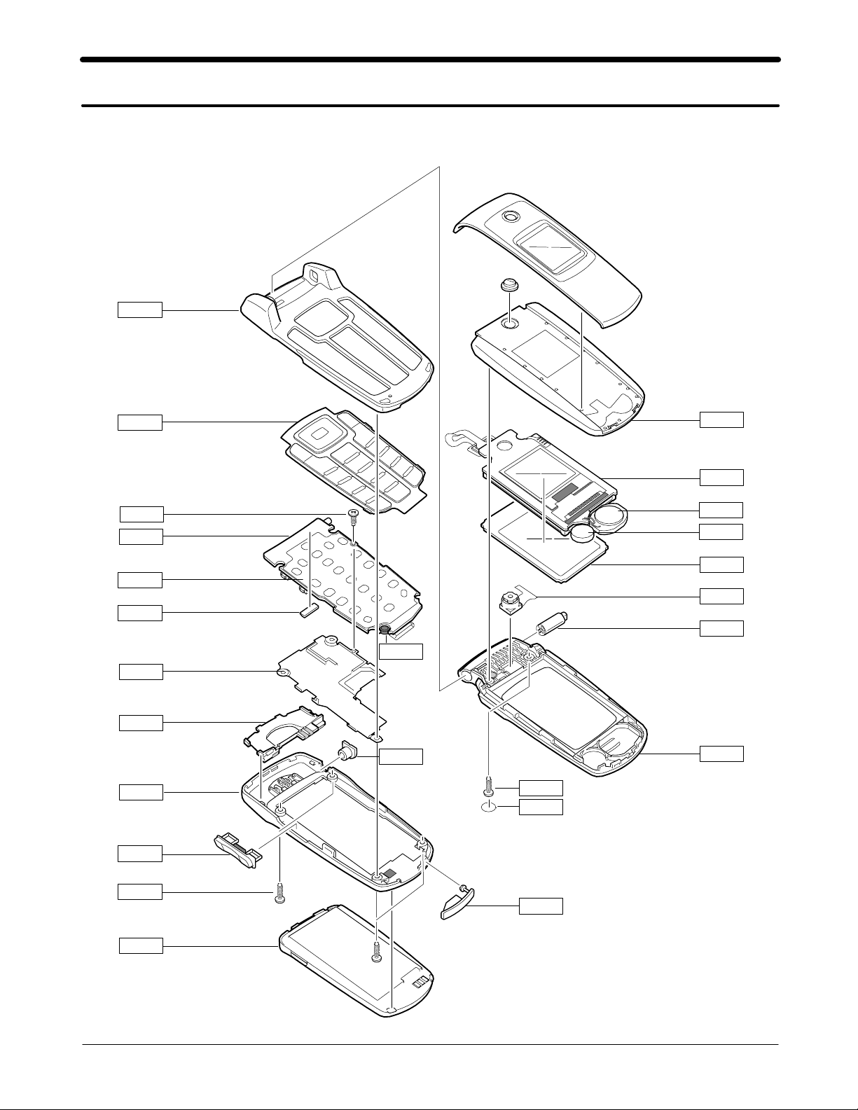
Exploded View and Parts List
2.
2-1.
Cellular phone Exploded View
QFR01
QKP01
QCR12
QMP01
QFU01
QLC01
QSP01
QMO01
QME01
QAN10
QSH01
QAN02
QRE01
QVO01
QCR12
QBA01
QMI01
QRF01
QMW01
QCA01
QHI01
QFL01
QCR12
QSC01
QRF03
2-1
SAMSUNG Proprietary-Contents may change without notice
This Document can not be used without Samsung's authorization
Exploded View and Parts List
2-2.
Cellular phone Parts list
Design LOC Discription SEC CODE
QAN02 INTENNA-SGH-M300 GH42-01219A
QAN10 ASSY-CUSHION-ANT CONTACT RUBBE GH98-01218A
QBA01 BATTERY-700MAH.MAIN,ENG,OCEAN GH43-02873A
QCA01 UNIT-CAMERA MODULE GH59-04349A
QCR12 SCREW-MACHINE
QCR12 SCREW-MACHINE
QCR12 SCREW-MACHINE
6001-001530
6001-001530
6001-001530
QFR01 ASSY CASE-FRONT GH98-04187B
QFU01 ASSY CASE-FOLDER UPPER GH98-04189B
QKP01 ASSY KEYPAD-(XET/EB) GH98-04194B
QME01 UNIT-DOME SHEET
KEY GH59-04499A
22
QMI01 MICROPHONE-ASSY-SGH_B600 GH30-00369A
QMO01 MOTOR DC-SGHS342I GH31-00119A
QMP01 PBA MAIN-SGH_M300 GH92-03849A
QRF01 PMO-COVER RF GH72-38610A
QSC01 MPR-SHEET SCREW CAP GH74-30953A
QSH01 ASSY CASE-SHIELD CAN GH98-04632A
QSP01 SPEAKER
3001-002153
QVO01 ASSY KEY-VOLUME GH98-05305A
QLC01 ELA UNIT-SGH-M300 LCD MODULE GH96-02546A
QMW01 ASSY COVER-MAIN WINDOW GH98-04255A
QRE01 ASSY CASE-REAR GH98-04191A
QRF03 PMO-COVER EAR IF GH72-38609A
QFL01 ASSY CASE-FOLDER LOWER GH98-04190A
QHI01 ASSY HINGE GH98-03590A
2-
SAMSUNG Proprietary-Contents may change without notice
This Document can not be used without Samsung's authorization
2
Exploded View and Parts List
Discription SEC CODE
BAG PE
6902-000297
ADAPTOR-SGHE690,SIL,EU,A_TYPE GH44-01361B
UNIT-20P,EARPHONE,SIL,B-TYPE GH59-04029B
LABEL(R)-WATER SOAK GH68-09361A
MANUAL USERS-EU GERMAN GH68-14617A
LABEL(R)-MAIN EU GH68-14836A
BOX(P)-UNIT MAIN EU GH69-05422A
MPR-SUB LCD CONN GAS GH74-10794A
MPR-REMOVE TAPE LCD GH74-13804A
MPR-LCD PCB MASK TAPE
B
GH74-15067A
MPR-TAPE LED GH74-17926A
MPR-INSU TAPE GH74-19264A
MPR-GASKET TAPE GH74-27014A
MPR-INSU TAPE SUB LCD GH74-27510A
MPR-INSU TAPE GH74-27512A
MPR-INSU TAPE GH74-29298A
MPR-TAPE MAIN FPCB GH74-30585A
MPR-INSU TAPE GH74-30759A
MPR-TAPE MAIN FPCB GH74-30860A
MPR-VINYL BOHO MAIN WINDOW GH74-31871A
MPR-VINYL BOHO MAIN WINDOW GH74-31987A
VINYL-BOHO MAIN GH74-32579A
TAPE GASK-LCD SIDE
A
GH74-32812A
TAPE-BACKLIGHT GH74-32834A
TAPE-MAIN WINDOW GH74-32837A
TAPE GH74-33042A
TAPE-PCB GASKET GH74-33071A
SPONGE GH74-33094A
TAPE INSU GH74-33095A
2-3
SAMSUNG Proprietary-Contents may change without notice
This Document can not be used without Samsung's authorization
Exploded View and Parts List
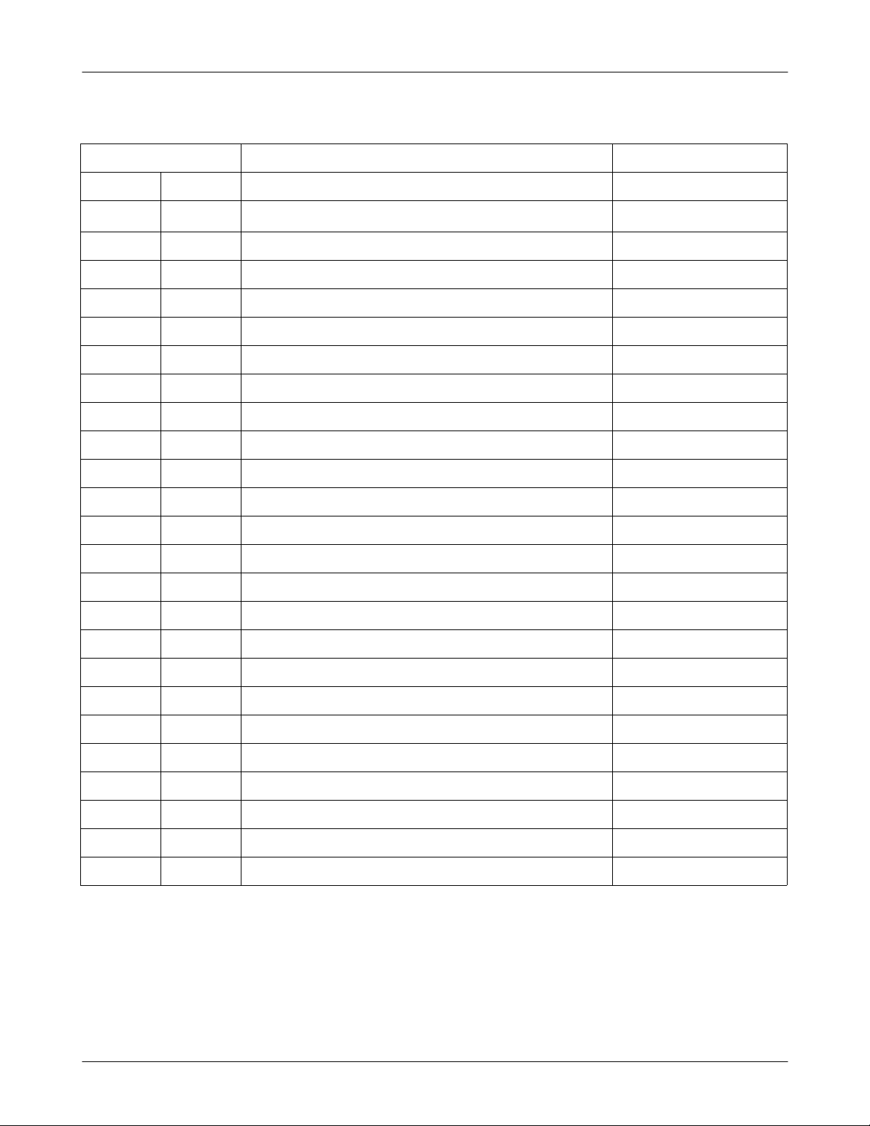
Disassembly
2-3.
1
Unscrew4points from the rear case
1)
Open the IF COVER
2)
caution
※
Be care of Shooting out damage and scratch
1)
not to occur.
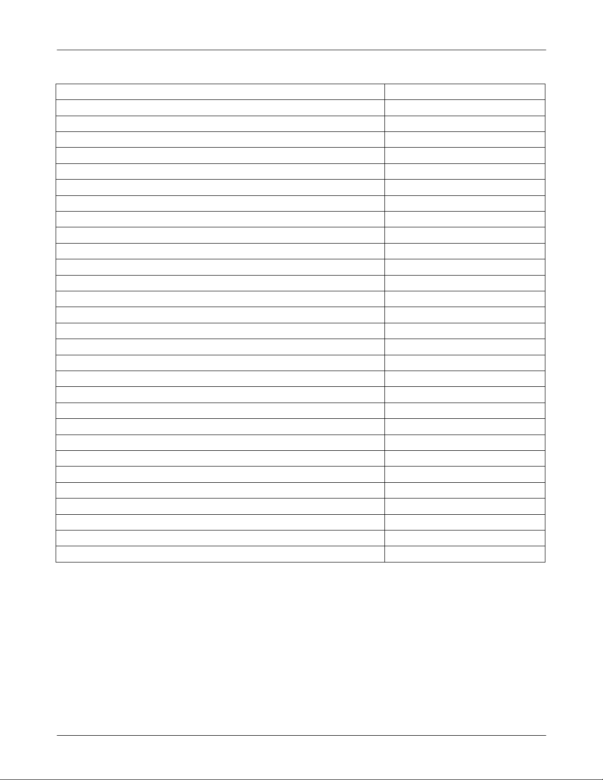
2
(1)
Disjoint from left low side to up side of rear
1)
case as below picture.
caution
※
When you disjointarear case, be care of
1)
Shooting out damage and scratch not to occur.
(2)
(3)
Remove the Volume key.
1)
Disjoint B'd from front case.
2)
caution
※
During disconnecting the B'd from FRONT, pay
1)
attention not to tear the LCD FPCB.
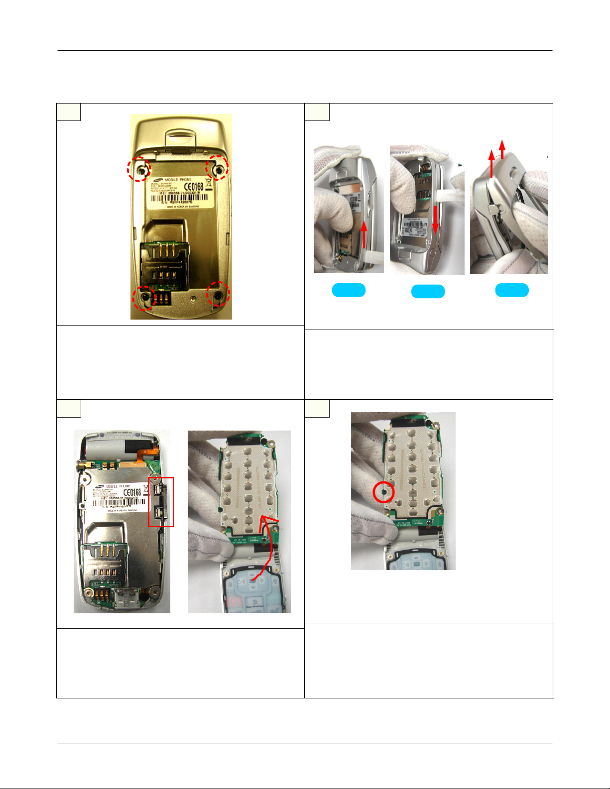
43
Remove the shield can screw
1)
Disjoint shield can from B'd
2)
caution
※
Pay attention not to damage for LCD FPCB
1)
during disconnecting the Shield can screw.
2-
SAMSUNG Proprietary-Contents may change without notice
This Document can not be used without Samsung's authorization
4
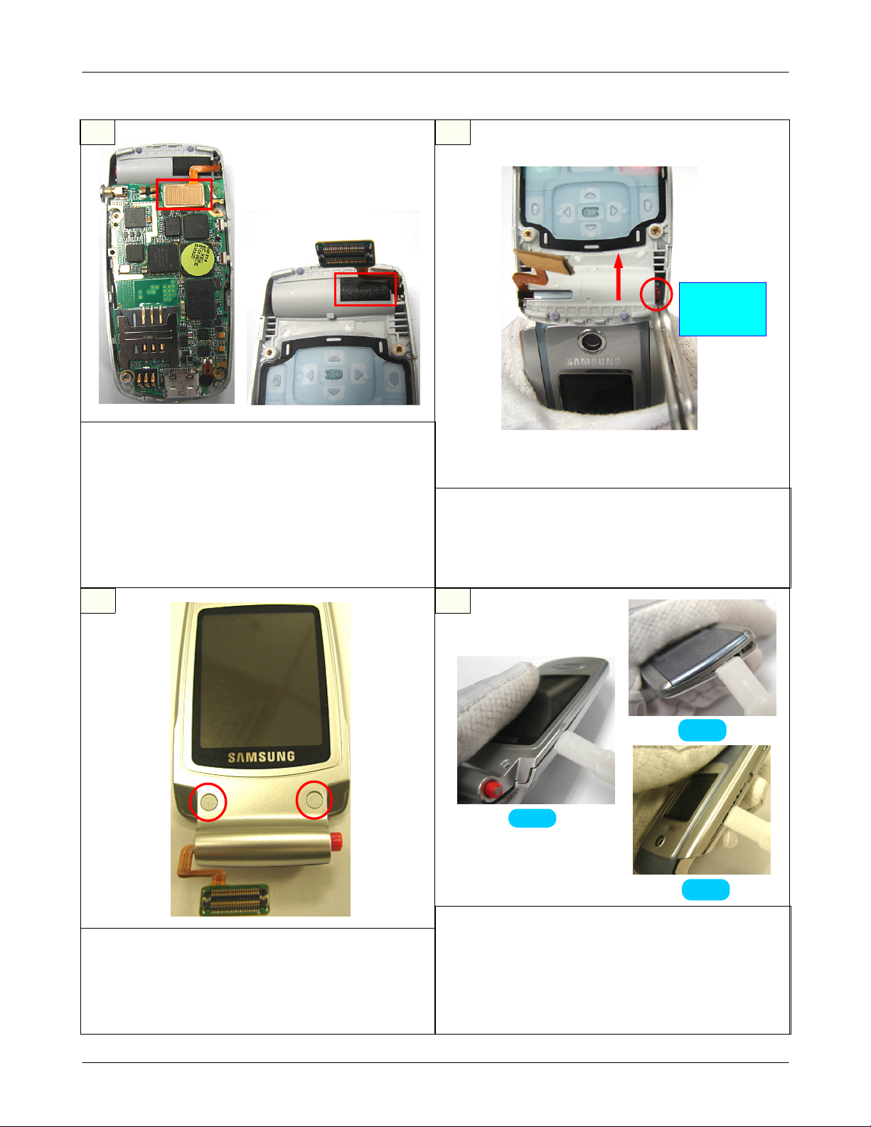
Exploded View and Parts List
5
Disconnect the LCD connecter and Disjoint the
1)
B'd
Remove the dust protection tape
2)
caution
※
Be care of Shooting out damage and scratch
1)
not to occur.
Pay attention not to damage for LCD FPCB.
2)
6
Press the
hinge
Pressing the hinge using the rounded tweezers
1)
or sort of thing, disjoint FRONT.
caution
※
Be care of Shooting out damage and scratch
1)
not to occur.
Remove screw cover using tweezers.
1)
Unscrew at the folder upper usingascrewdriver
2)
caution
※
Be care of Shooting out damage and scratch
1)
not to occur.
87
(2)
(1)
(3)
After disjoint the hooker of the lower side,
1)
disassemble the LOWER case as below the
picture
.
caution
※
Be care of Shooting out damage and scratch
1)
not to occur.
2-5
SAMSUNG Proprietary-Contents may change without notice
This Document can not be used without Samsung's authorization
Exploded View and Parts List
9
Remove the Speaker/Motor in the LOWER.
1)
Remove the LCD in the LOWER.
2)
caution
※
Be care of Speaker/Motor wire cracking or
1)
damage.
10
Check the separated plastics.
1)
caution
※
Check all of the material is taped.
1)
2-
SAMSUNG Proprietary-Contents may change without notice
This Document can not be used without Samsung's authorization
6
2-4.
Exploded View and Parts List
Assembly
1
Arrange
the wire
1) Put the LOWER hinge hall to the LCD
FPCB, and then put the camera to the
PCB.
2) Put the Speaker to the LOWER case,
and then arrange the Wire. Put the
speaker to the LOWER case, right side
slightly.
caution
※
Be care of SPEAKER/MOTOR wire cracking or
1)
damage.
2
Joint folder hinge side of UPPER case.
1)
Joint folder UPPER case side and edge.
2)
caution
※
Be care of Shooting out damage and scratch
1)
not to occur.
43
Screw two point of FOLDER Ass'y.
1)
Assemble the SCREW COVER
2)
caution
※
Be care of Shooting out damage and scratch
1)
not to occur.
SAMSUNG Proprietary-Contents may change without notice
This Document can not be used without Samsung's authorization
Put the FPCB to the FRONT hole.
1)
Pressing the red colored hinge, assembly
2)
the folder and FRONT case
caution
※
Pay attention not to damage for LCD FPCB.
1)
2-7
Exploded View and Parts List
5
Attach anti-dust TAPE
1)
LetaKEY PAD on front assy.
2)
caution
※
Be care of Shooting out damage and scratch
1)
not to occur.
Pay attention not to damage for LCD FPCB.
2)
6
LockaLCD CONNECTOR to PBA
1)
caution
※
Assemble the LCD connect horizontally.
1)
Pay attention not to damage for LCD FPCB.
2)
joint the
hook
Scwering
Joint the shield can right hook and
1)
hole of the B'd.
Screw the left hall of the B'd.
2)
caution
※
Pay attention not to damage for LCD FPCB.
1)
87
oint the
hook
Joint the FRONT upper hook and B'd and
1)
arrange the B'd, FRONT.
Attach the Volume Key.
2)
caution
※
Pay attention not to damage for LCD FPCB.
1)
Confirm B'd is attached completely on the
2)
FRONT.
2-
SAMSUNG Proprietary-Contents may change without notice
This Document can not be used without Samsung's authorization
8
Exploded View and Parts List
9
Joint REAR case
and FRONT case.
As below picture, joint the REAR upper
1)
and FRONT and ASS'Y.
Joint the REAR case side, and then edge.
2)
caution
※
Be care of Shooting out damage and scratch
1)
not to occur.
10
Screw4point on REAR assy'.
1)
Attach the RF COVER.
2)
caution
※
Be care of Shooting out damage and scratch
1)
not to occur.
2-9
SAMSUNG Proprietary-Contents may change without notice
This Document can not be used without Samsung's authorization

Exploded View and Parts List
LCD KIT ASSEMBLING
2-5.
1
Attach
conductive
Tape
Attach conduction tape on the left and right
1)
side of LCD.
Attach isolation tape on the left and right side
2)
of LCD.
caution
※
When you attach the tape, be careful ofabase
1)
line ofapicture.
Attach
isolation Tape
2
Taping silk
line
Attach the SPONGE along the line.
1)
Attach the isolation tape along the line.
2)
caution
※
When you attach the tape, be careful ofabase
1)
line ofapicture.
Taping silk
line
camera connect
sticky isolation
Tape
Attach CAMERA CONNECTOR sticky isolation
1)
tape
.
caution
※
When you attach the tape, be careful ofabase
1)
line ofapicture.
43
Attach the GASKET on the LCD CONNECTOR
1)
caution
※
When you attach the tape, be careful ofabase
1)
line ofapicture.
Tape should be in the LCD connect.)
(
2-
SAMSUNG Proprietary-Contents may change without notice
This Document can not be used without Samsung's authorization
10
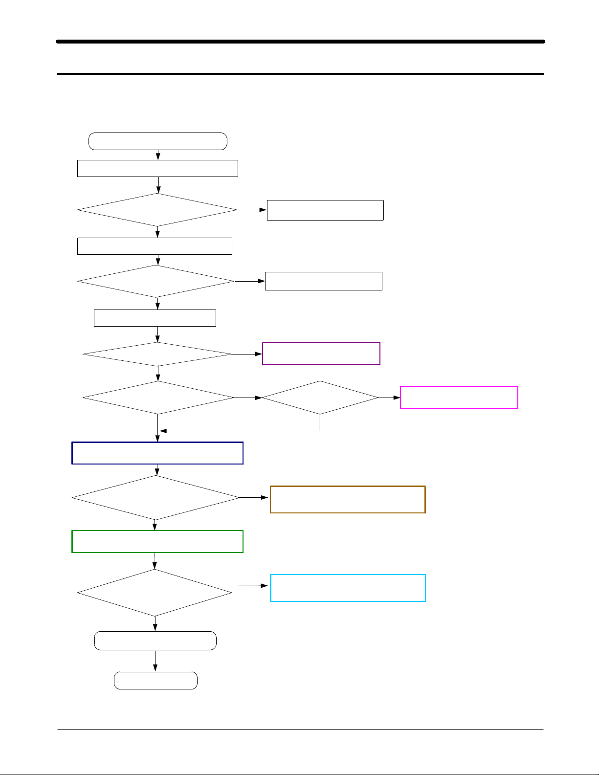
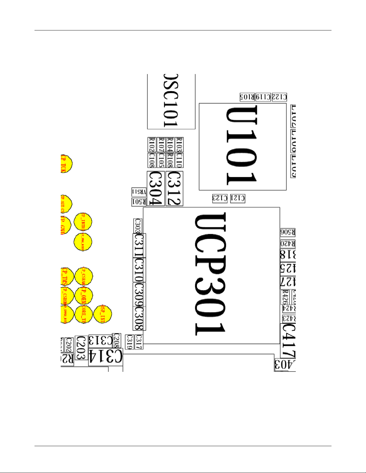
3. Flow Chart of Troubleshooting
Baseband
3-1.
3-1-1.
Power ON
Power On' does not work
'
Check the current consumption
Yes
Current consumption
Check the Vbat Voltage
Voltage
Check the pin of UCP
Pin#J12
Pin#A13 and pin#A14
>= 100
=2.8V
mA
Yes
>=3.3V
Yes
>= 2.8V
Yes
301
No
No
No
No
Download again
Charge the Battery
Check UCP
301
pin#G11
and
C313
=1.8V
No
Check UCP
301
and
C314
Yes
Check the clock signal at pin#
Freq
Vrms
Vpp
Check the clock signal at pin#8of
Freq
Check the initial operation
≒
END
=26
>=300
900
=13
MHz
mV
Yes
Mz
Yes
mV
30 #31ofU101
U101
No
No
Yes
Check the clock generation circuit
relatedtoOSC
(
Check
101)
U101
3-1
SAMSUNG Proprietary-Contents may change without notice
This Document can not be used without Samsung's authorization
Flow Chart of Troubleshooting
3-2
SAMSUNG Proprietary-Contents may change without notice
This Document can not be used without Samsung's authorization
Flow Chart of Troubleshooting
N
2
0
V
I
_
1
4
0
1
1
4
T
B
A
R
B
2
V
3
_
C
T
R
V
5
0
3
R
V
8
.
1
_
D
C
C
V
9
V
.
2
_
D
C
C
V
V
9
.
2
_
F
R
V
V
9
.
2
_
A
C
C
V
V
9
.
2
_
B
C
C
V
A
T
T
T
K
S
O
S
A
L
I
R
R
D
C
_
_
M
M
M
M
M
I
I
I
I
I
S
S
S
S
4
0
3
C
T
A
B
V
1
0
3
V
9
.
2
_
D
C
C
V
V
9
.
2
_
A
C
C
V
V
9
.
2
_
D
C
C
V
C
3
0
3
C
2
0
3
C
1
3
1
1
J
C
2
4
1
3
D
D
D
D
V
V
5
D
D
V
1
C
0
6
V
D
7
D
B
1
3
Q
D
N
G
E
8
_
S
1
P
C
1
B
5
_
S
2
P
C
1
K
5
R
U
_
C
H
1
F
1
1
D
D
V
J
3
2
D
D
V
3
M
3
D
D
V
6
N
1
I
D
_
O
D
5
N
2
I
D
_
O
D
J
4
V
S
S
1
5
G
V
S
S
2
4
K
V
S
S
3
2
R
V
S
S
4
P
6
V
D
D
D
1
N
1
D
D
N
G
1
M
0
V
B
D
D
6
A
B
D
N
G
F
6
V
V
D
D
1
L
1
G
V
D
N
P
1
3
T
L
C
O
_
4
C
O
T
_
L
C
4
B
3
A
C
_
D
D
3
1
G
S
D
N
1
F
7
S
D
N
2
G
F
8
S
D
N
3
G
F
9
S
D
N
4
G
0
F
1
S
D
N
5
G
7
G
S
D
N
6
G
8
G
S
D
N
7
G
9
G
S
D
N
8
G
0
1
G
G
S
D
N
9
6
H
D
N
S
0
1
H
7
D
N
S
1
1
H
8
D
N
S
2
1
H
9
D
1
N
S
3
J
7
D
1
N
S
4
J
8
D
1
N
S
5
J
9
D
1
N
S
6
J
1
0
D
1
N
S
7
1
K
0
5
C
N
1
6
C
N
2
S
0
0
1
1
9
1
1
1
1
N
P
R
K
J
T
T
O
K
O
I
I
S
S
L
_
_
R
R
C
P
M
_
_
_
I
U
P
P
S
M
I
U
U
S
D
N
G
D
N
G
D
N
G
V
V
V
D
D
D
N
G
X
U
A
G
G
G
G
G
G
G
G
1
2
3
4
5
1
1
1
1
1
B
B
B
B
B
D
D
D
D
D
3
2
3
2
3
F
E
E
D
D
)
)
)
)
)
4
5
1
2
3
1
1
1
1
1
(
(
(
(
(
B
B
B
B
B
D
D
D
D
D
_
_
_
_
_
P
P
P
P
P
S
S
S
S
S
D
D
D
D
D
1
K
L
L
B
C
_
_
M
T
I
Y
M
I
S
4
1
K
K
L
C
_
M
I
S
0
9
1
B
B
D
D
1
2
F
F
)
)
0
9
1
(
(
B
B
D
D
_
_
P
P
S
S
D
D
O
S
E
V
K
M
2
3
2
1
2
1
1
H
K
M
I
S
V
8
B
D
4
4
F
G
)
)
7
8
(
(
B
B
D
D
_
_
P
P
S
S
D
D
4
3
5
1
1
1
9
1
1
1
C
A
F
G
G
F
C
6
7
V
C
V
V
V
_
_
T
R
R
R
R
O
O
R
D
D
D
D
D
D
_
V
_
_
_
L
L
2
1
B
G
I
V
V
D
D
N
V
I
E
E
R
L
L
7
B
D
0
1
4
2
3
5
6
B
B
B
B
B
B
B
D
D
D
D
D
D
D
5
3
1
2
3
6
5
J
J
K
K
K
H
G
)
)
)
)
)
)
)
4
5
6
0
1
2
3
(
(
(
(
(
(
(
B
B
B
B
B
B
B
D
D
D
D
D
D
D
_
_
_
_
_
_
_
P
P
P
P
P
P
P
S
S
S
S
S
S
S
D
D
D
D
D
D
D
1
5
1
3
C
4
1
3
C
3
1
3
C
2
1
3
C
1
1
3
C
0
1
3
C
9
0
3
C
8
0
3
C
K
L
I
1
2
L
L
E
E
S
S
_
_
D
D
N
N
A
A
B
B
0
2
1
3
2
0
2
1
1
1
1
1
1
1
A
B
D
A
B
J
B
3
2
5
4
A
B
A
B
_
_
_
_
_
_
_
_
O
O
O
O
S
S
S
S
4
4
5
5
L
V
D
D
D
D
L
L
L
L
L
L
L
V
V
V
V
V
V
V
O
S
C
D
D
C
S
S
S
_
_
_
_
P
P
P
P
U
U
U
U
T
A
B
V
1
4
1
G
7
7
8
1
8
L
M
N
F
K
1
C
C
C
C
_
S
S
C
S
O
P
P
A
P
_
_
D
_
V
L
N
O
K
V
L
S
D
C
C
S
S
4
4
1
3
2
1
1
1
1
1
E
E
E
F
D
T
S
T
V
C
N
X
E
A
E
S
R
E
B
P
S
R
D
I
V
_
_
V
B
I
_
H
_
D
H
C
H
S
C
C
1
0
3
P
C
U
P
S
C
_
N
T
2
3
0
4
1
5
6
L
L
L
L
L
L
8
B
A
7
5
K
K
)
8
(
B
A
_
P
S
D
B
B
B
B
B
B
B
A
A
A
A
A
A
A
2
1
1
1
2
5
L
P
N
N
M
M
)
)
)
)
)
)
)
3
4
5
6
7
1
2
(
(
(
(
(
(
(
B
B
B
B
B
B
B
A
A
A
A
A
A
A
_
_
_
_
_
_
_
P
P
P
P
P
P
P
S
S
S
S
S
S
S
D
D
D
D
D
D
D
C
E
W
B
O
|
R
I
O
R
A
3
6
2
6
3
L
L
E
K
R
)
0
(
B
A
_
P
S
D
E
N
T
S
0
1
3
2
4
6
5
7
L
T
T
T
T
T
T
C
C
C
C
C
C
O
O
O
O
O
O
5
5
5
6
4
3
F
E
C
A
B
G
M
R
A
L
F
A
E
C
T
R
V
R
7
1
3
C
0
5
0
0
1
1
1
1
9
H
A
E
D
E
F
F
1
2
N
E
E
X
X
M
R
R
U
U
L
V
C
A
A
A
_
_
_
C
C
C
_
V
R
G
E
_
I
N
B
N
D
D
T
A
A
R
Q
T
I
N
R
K
_
E
E
P
R
P
W
E
D
O
M
E
E
R
S
_
O
T
P
F
S
_
U
B
W
1
1
W
N
S
_
P
R
W
2
W
S
_
P
R
W
T
I
R
N
D
7
C
N
C
M
X
E
Q
O
A
N
_
L
C
C
K
T
R
O
I
D
A
D
I
I
D
A
D
N
I
R
A
D
K
I
C
A
D
N
G
V
E
R
P
G
V
E
R
V
X
V
C
M
X
U
U
O
N
T
A
X
U
U
O
P
T
A
X
U
N
I
A
N
X
U
P
I
A
N
T
U
O
N
I
C
M
T
U
O
P
I
C
M
I
N
I
N
C
M
I
P
I
N
C
M
N
B
T
U
O
A
P
B
T
U
O
A
T
N
U
O
A
A
P
A
T
U
O
A
X
X
N
R
T
Q
X
X
P
R
T
Q
X
X
R
T
I
N
X
X
R
T
I
P
F
E
1
R
A
R
F
E
2
R
A
R
P
X
T
C
F
1
7
E
L
L
T
R
C
E
S
O
1
3
B
A
A
2
K
A
E
C
D
L
R
R
R
E
E
E
S
S
S
2
1
2
C
C
A
P
E
E
K
N
_
Q
E
_
R
R
T
T
B
S
I
W
N
V
R
P
I
P
E
E
K
_
Q
R
R
T
W
N
P
I
_
_
P
P
T
T
9
L
1
0
L
9
M
1
N
0
9
K
7
L
1
C
5
1
C
4
3
P
5
P
6
R
1
D
4
N
6
M
6
L
4
P
4
R
1
R
4
1
M
3
1
R
3
1
3
L
1
K
3
1
4
L
1
M
5
1
P
5
1
N
5
4
1
M
1
N
4
1
P
2
1
R
2
1
N
2
1
P
1
6
C
7
C
6
D
7
D
6
B
5
B
7
E
9
D
R
N
_
O
G
N
_
O
P
T
_
N
I
M
C
_
M
K
3
2
K
8
1
3
C
O
N
U
T
O
U
T
P
X
I
N
N
X
I
N
P
O
N
U
T
O
U
T
P
I
C
I
N
N
I
C
I
N
P
B
U
N
T
U
T
B
P
A
U
N
T
U
T
A
P
X
Q
T
_
N
X
Q
T
_
P
R
T
_
R
X
I
N
X
T
_
R
I
P
P
R
_
W
X
C
A
F
)
)
0
(
2
(
W
L
O
O
R
C
_
_
Y
Y
E
E
K
K
1
0
3
R
T
2
3
1
P
W
J
I
S
D
C
1
L
3
K
C
L
A
X
U
A
U
X
U
A
A
U
M
I
C
I
C
M
M
M
A
O
O
A
A
O
O
A
R
T
9
1
3
C
3
2
N
O
)
5
1
:
0
(
B
D
_
P
S
D
)
8
:
0
(
B
A
_
P
S
D
I
_
W
P
R
_
S
P
D
S
D
A
N
T
E
S
E
R
_
H
S
A
L
F
N
N
S
S
E
E
N
E
A
A
_
_
_
E
P
D
M
O
F
O
M
X
A
M
V
T
N
E
N
K
L
L
A
E
E
_
_
R
C
D
F
X
E
R
R
T
R
S
E
E
S
S
3-3
SAMSUNG Proprietary-Contents may change without notice
This Document can not be used without Samsung's authorization
Flow Chart of Troubleshooting
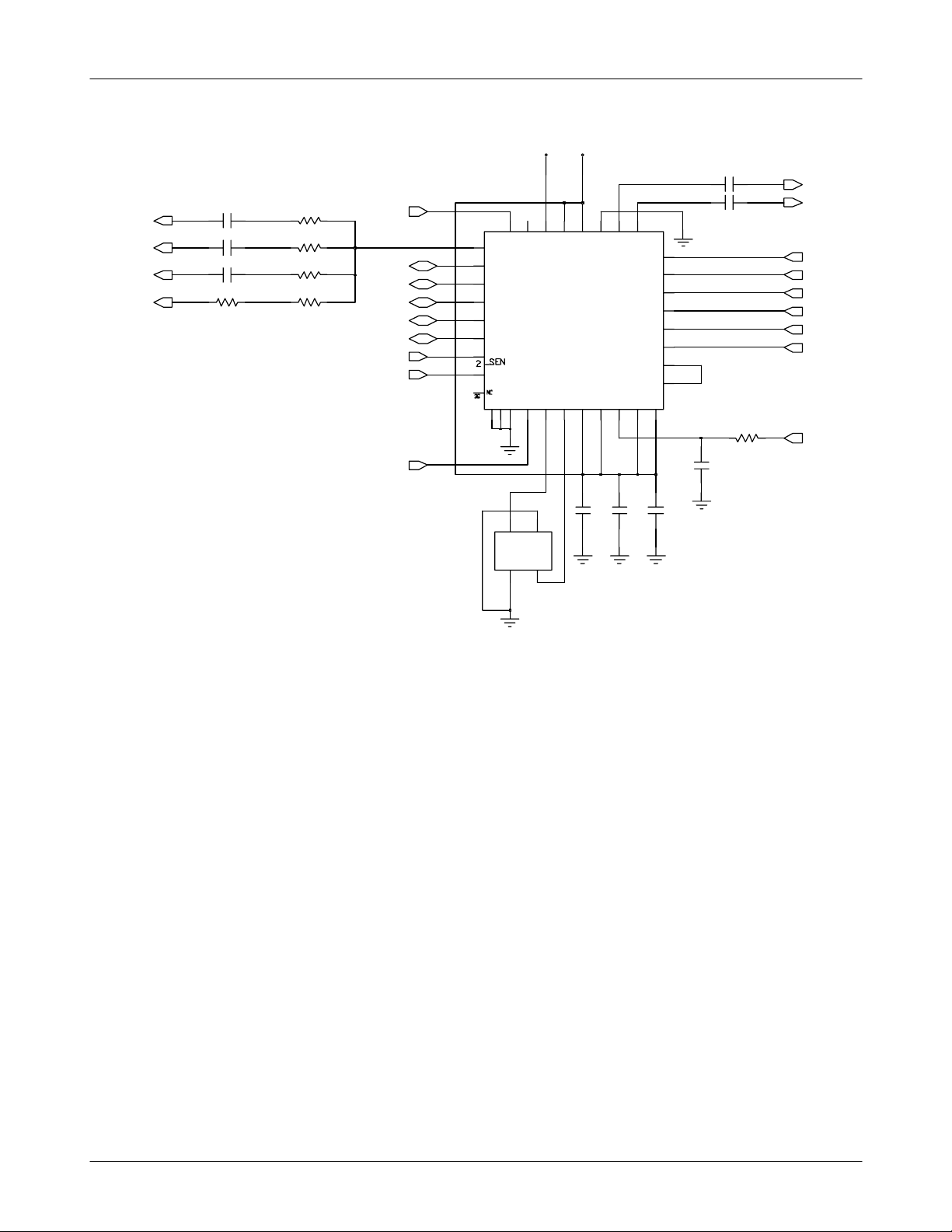
VRF_2.9VVCCD_2.9V
CLK13M_TR
CLK13M_MC
CLK13M_YMU
CLK13M_AIT701X
C105
C108
C110
R108
R107
R102
R103
R104
RF_EN
RTX_IP
RTX_IN
RTX_QP
RTX_QN
SERDAT
SERLE
SERCLK
XOENA
C102
C104
9
10
T
N
E
D
S
P
E
_
XOUT
BIP
BIN
BQP
BQN
SDIO
SCLK
R
_
D
C
C
N
N
N
G
3435
33
OSC101
3
GND2
HOT
8
7
6
5
4
3
1
GND1
2
N
E
X
HOT
13
11
12
D
O
I
D
V
V
U101
2
1
L
L
A
A
T
T
X
X
31
30
29
4
1
16
15
14
L
D
D
V
D
D
V
28
H
D
O
N
O
F
F
G
R
R
RFIPP
17
RFIPN
18
RFIDP
19
RFIDN
20
RFIEP
21
RFIEN
22
RFIAP
23
RFIAN
E
24
V
D
I
D
D
V
27
O
C
D
F
M
X
A
X
2632
C122
25
C123C121
R105
C119
GSM_PAM_IN
DPCS_PAM_IN
PCS_LNA_IN_P
PCS_LNA_IN_N
DCS_LNA_IN_P
DCS_LNA_IN_N
GSM_LNA_IN_P
GSM_LNA_IN_N
AFC
3-4
SAMSUNG Proprietary-Contents may change without notice
This Document can not be used without Samsung's authorization
 Loading...