

Page 1
Global LCD Panel Exchange Center
AT32
DATE OF ISSUE
EXTENSION CODE
Prepared by
LCD Sales & Marketing Team
Samsung Display Co., Ltd
www.panelook.com
Product Specification
( ) Preliminary Specification
( √ ) Approval Specification
Any Modification of Spec is not allowed without SDC’s permission.
CUSTOMER
MODEL NO. LTN156
2013.04.02
Customer Approval & Feedback
-L01
Approved by
One step solution for LCD / PDP / OLED panel application: Datasheet, inventory and accessory!
www.panelook.com
Page 2
Global LCD Panel Exchange Center
www.panelook.com
————————————————————————————————————————————————–
Table of Contents
1. GENERAL DESCRIPTION ............................................................................................................................................. 3
2. ABSOLUTE MAXIMUM RATINGS ............................................................................................................................ 5
ENVIRONMENTAL ABSOLTE RATINGS ................................................................................................................... 5
2.1
2.2
ELECTRICAL ABSOLUTE RATINGS ........................................................................................................................... 6
2.3
THE OTHERS .............................................................................................................................................................. 6
3. OPTICAL CHARACTERISTICS ..................................................................................................................................... 7
4. BLOCK DIAGRAM ....................................................................................................................................................... 10
TFT LCD MODULE ................................................................................................................................................... 10
4.1
4.2
THE STRUCTURE OF LED PLACEMENT.................................................................................................................. 10
5. ELECTRICAL CHARACTERISTICS ............................................................................................................................. 11
TFT LCD MODULE ................................................................................................................................................... 11
5.1
5.2
BACK LIGHT UNIT ................................................................................................................................................... 13
5.3
LED DRIVER .............................................................................................................................................................. 13
5.4
LVDS INTERFACE ..................................................................................................................................................... 15
5.5
INTERFACE TIMING ................................................................................................................................................ 17
5.6
INPUT COLOR DATA MAPPING............................................................................................................................. 18
5.7
POWER ON/OFF SEQUENCE ................................................................................................................................. 19
5.8
INPUT TERMINAL PIN ASSIGNMENT .................................................................................................................... 21
6. PIXEL FORMAT ............................................................................................................................................................ 22
7. OUTLINE DIMENSION ............................................................................................................................................... 23
8. RELIABILITY TEST ....................................................................................................................................................... 24
——————————————————————————————————————————————––—
Doc.No. LTN156AT32-L01 Page 2 of 24 Rev.No. 05-A00-G-130402
One step solution for LCD / PDP / OLED panel application: Datasheet, inventory and accessory!
www.panelook.com
Page 3
Global LCD Panel Exchange Center
Item
Specification
Unit
Note
Display area
344.232 (H) x 193.536 (V) (15.6”diagonal)
mm
Driver Element
a-Si TFT active matrix
Display colors
262,144 (6bit)
Number of pixel
1366 *768(HD)
Pixel
16:9
Pixel Arrangement
RGB vertical stripe
Pixel pitch
0.252 (H) x 0.252 (V) (TYP.)
mm
Display Mode
Normally white, TN mode
Thickness of glass
0.5
mm
Surface treatment
Haze 0, Hardness 3H
Glare
Environmental safe regulation
Pb Free, Halogen Free
Power Consumption
Total 4.16W(Typ) @Logic 0.7W(Typ) BLU 3.46W (Typ)
Total 4.4W(Max)
Mosaic
PTN
www.panelook.com
————————————————————————————————————————————————–
1. GENERAL DESCRIPTION
DESCRIPTION
The LTN156AT32-L01 uses a color active matrix TFT (Thin Film Transistor) liquid crystal display (LCD) that uses
amorphous silicon TFTs as switching components. This model is composed of a TFT LCD panel, a driver circuit,
and a backlight unit. This 15.6” model has a resolution of 1366 x 768 pixels and can display up to 262,144
colors.
FEATURES
High contrast ratio
HD (1366 x 768 pixels) resolution
Low power consumption
Fast Response
LED back light with an embedded LED driver
DE (Data enable) only mode
3.3V LVDS Interface
Onboard EDID chip
APPLICATIONS
Notebook PC
If the intent to use this product is for other purpose, please contact Samsung Display.
GENERAL INFORMATION
——————————————————————————————————————————————––—
Doc.No. LTN156AT32-L01 Page 3 of 24 Rev.No. 05-A00-G-130402
One step solution for LCD / PDP / OLED panel application: Datasheet, inventory and accessory!
www.panelook.com
Page 4
Global LCD Panel Exchange Center
Item
Min.
Typ.
Max.
Unit
Note
Module
Horizontal (H)
358.8
359.3
359.8
mm
Vertical (V)
209.0
209.5
210.0
mm
Depth (D)
-
5.0
5.5
mm
(1)
Weight
-
440
450 g
www.panelook.com
————————————————————————————————————————————————–
MECHANICAL INFORMATION
Size
NOTE (1) Measuring method for thickness
Force to be applied for measurement (Panel body) : by using the micrometer.
Force to be applied for measurement (PCB side) : The 50gf when using the height gauge.
——————————————————————————————————————————————––—
Doc.No. LTN156AT32-L01 Page 4 of 24 Rev.No. 05-A00-G-130402
One step solution for LCD / PDP / OLED panel application: Datasheet, inventory and accessory!
www.panelook.com
Page 5
Global LCD Panel Exchange Center
Item
Symbol
Min.
Max.
Unit
Note
Storage temperate
TSTG
-20
60
qC
(1)
Operating temperature
(Temperature of glass surface)
Shock ( non-operating )
Snop 240 G (2), (4)
Vibration (non-operating)
Vnop 2.41
G
(3), (4)
www.panelook.com
————————————————————————————————————————————————–
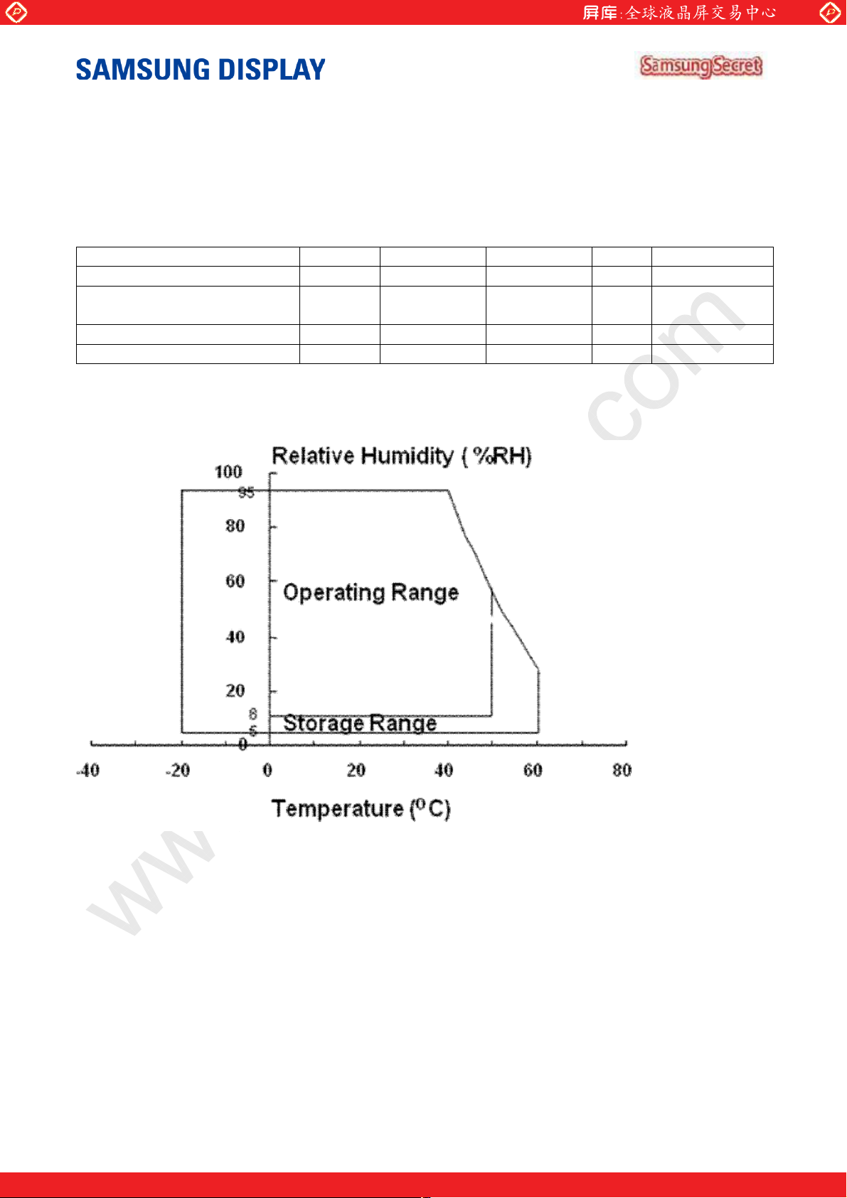
2. ABSOLUTE MAXIMUM RATINGS
2.1 ENVIRONMENTAL ABSOLTE RATINGS
TOPR
Note (1) The range of temperature and relative humidity are shown in the graph below 95% RH Max. .
(39 ≥ Ta) If the temperature is higher than 40 ଇ, the maximum temperature of wet–bulb shall be
less than 39ଇ. No condensation
0 50 qC
(1)
(2) Vibrate rX, rY, and r Z axis in the shape of the half sine wave one time for 2ms .
(3) Vibrate the X, Y, and Z randomly within a 5 - 500 Hz range for 30min.
(4) When testing a vibration and a shock, the fixture, which holds the module to be tested shall be
hard and rigid in order for the the module not to be twisted or bent by the fixture.
——————————————————————————————————————————————––—
Doc.No. LTN156AT32-L01 Page 5 of 24 Rev.No. 05-A00-G-130402
One step solution for LCD / PDP / OLED panel application: Datasheet, inventory and accessory!
www.panelook.com
Page 6
Global LCD Panel Exchange Center
Item
Symbol
Min.
Max.
Unit
Note
Power Supply Voltage
VLCD_VCC
VSS - 0.3
4.0
LVDS Input Voltage
VLVDS
VSS - 0.3
2.0
Item
Symbol
Min.
Max.
Unit
Note
BLU Supply Voltage
V
BL_PWR
VSS - 0.3
26.5
V
(1), (2)
BLU Supply Current
(1), (2)
Duty 100%
Item
Test Conditions
Remark
CONTACT DISCHARGE
150pF, 330:, r 8kV, 200points, 1 time/point
Operating
AIR DISCHARGE
150pF, 330:, r 15kV, 200points, 1 time/point
Operating
www.panelook.com
————————————————————————————————————————————————–
2.2 ELECTRICAL ABSOLUTE RATINGS
(1) TFT LCD MODULE
V
Note (1) Within Ta (25 r 2 qC )
(2) Permanent damage to the device may occur if exceed maximum values
.
(2) BACKLIGHT UNIT
I
BL_PWR
LCD_VCC =3.3V, V
V
- 0.96 A
= GND = 0V
SS
(1),(2)
VSS = GND = 0V
Vin=12V
Note (1) Within Ta (25 r 2 qC )
(2) Permanent damage to the device may occur if exceed maximum values
2.3 THE OTHERS
(1) STATIC ELECTRICITY PRESSURE RESISTANCE
——————————————————————————————————————————————––—
Doc.No. LTN156AT32-L01 Page 6 of 24 Rev.No. 05-A00-G-130402
One step solution for LCD / PDP / OLED panel application: Datasheet, inventory and accessory!
www.panelook.com
Page 7
Global LCD Panel Exchange Center
Item
Symbol
Condition
Min.
Typ.
Max.
Unit
Note
Contrast Ratio
CR
Normal
300
500 - -
(1),(2),(5)
Response time
( Rising + Falling )
Average Luminance
of White
(5 Points)
IF=100%
(1),(4)
Chromaticit
Red
RX
0.619
RY
0.350
Gree
n
GX
0.340
GY
0.600
Blue
BX
0.154
BY
0.095
Whit
e
WX
0.313
WY
0.329
Hor.
TL
At center
40
45
-
Degrees
TH
40
45
-
Ver.
IH
10
15
-
IL
30
35
-
Color
Gamut
tion
13P - -
1.66
5P
1.25
www.panelook.com
————————————————————————————————————————————————–
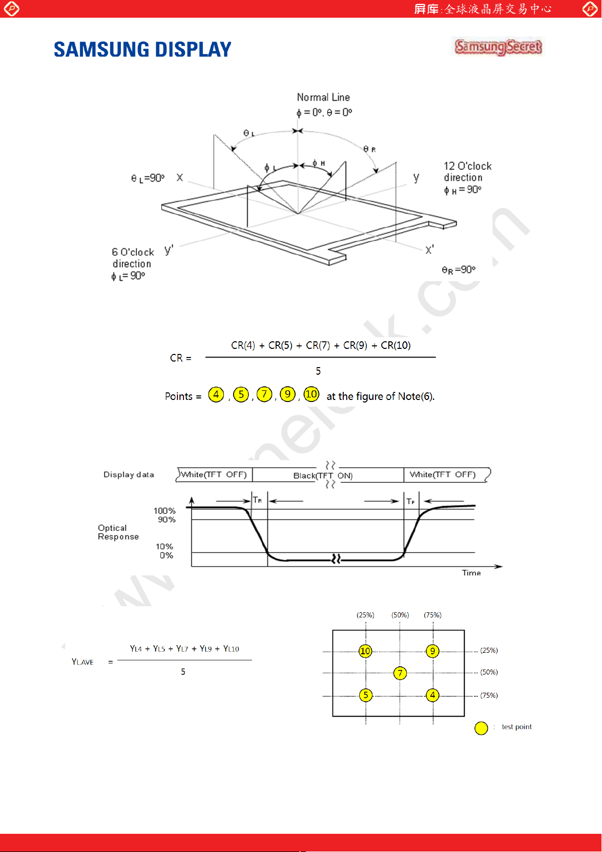
3. OPTICAL CHARACTERISTICS
The following items are measured under the stable conditions.* The optical characteristics should be measured
in the dark room or the equivalent environment by the methods shown in the Note (5).
Measuring equipment : TOPCON SR-3
Ta = 25 r 2 qC, V
TRT
Color
y
(CIE)
YL,AVE
Viewing
Angle
I = 0
T = 0
LCD_VCC =3.3V, fv= 60Hz, fDCLK = 72.33MHz, IF = 100% duty
- 16 25 msec
190 220 - cd/m
-0.03
+0.03
2
(1),(5)
(1),(3)
Duty
Viewing
Angle
White varia
CR t 10
(1),(5)
CG - 60 - %
GL
(6)
One step solution for LCD / PDP / OLED panel application: Datasheet, inventory and accessory!
——————————————————————————————————————————————––—
Doc.No. LTN156AT32-L01 Page 7 of 24 Rev.No. 05-A00-G-130402
www.panelook.com
Page 8
Global LCD Panel Exchange Center
www.panelook.com
————————————————————————————————————————————————–
Note (1) The definition of viewing angle: The range of viewing angle (10 d C/R)
Note (2) The definition of contrast ratio (CR): The ratio of max. gray and min gray at 5 points
(4, 5, 7, 9, and 10)
Note (3) The definition of Response time: Subtotal of the time, during which the transmission changes from
10% to 90% when the TFT turns on and off.
Note (4) The definition of average luminance of white: Measure the luminance of white at 5 points.
——————————————————————————————————————————————––—
Doc.No. LTN156AT32-L01 Page 8 of 24 Rev.No. 05-A00-G-130402
One step solution for LCD / PDP / OLED panel application: Datasheet, inventory and accessory!
www.panelook.com
Page 9

Global LCD Panel Exchange Center
G L =
Maximum luminance of 13 points
Minimum luminance of 13 points
www.panelook.com
————————————————————————————————————————————————–
Note (5) Measure the panel, which is left for 30 min. at the normal temp. after leaving it for 30 min with turning
the back light on at the rating. The measurement should be executed under the condition including
the ambient temp., 25ଇ±2ଇ, the dark room, windless (removed the direct wind), and no vibration.
Note (6) The definition of white variation at 13 points (G L )
——————————————————————————————————————————————––—
Doc.No. LTN156AT32-L01 Page 9 of 24 Rev.No. 05-A00-G-130402
One step solution for LCD / PDP / OLED panel application: Datasheet, inventory and accessory!
www.panelook.com
Page 10

Global LCD Panel Exchange Center
www.panelook.com
————————————————————————————————————————————————–
4. BLOCK DIAGRAM
4.1 TFT LCD MODULE
4.2 THE STRUCTURE OF LED PLACEMENT
(4 channel x 1ea = 4ea)
——————————————————————————————————————————————––—
Doc.No. LTN156AT32-L01 Page 10 of 24 Rev.No. 05-A00-G-130402
One step solution for LCD / PDP / OLED panel application: Datasheet, inventory and accessory!
www.panelook.com
Page 11

Global LCD Panel Exchange Center
Item
Symbol
Min.
Typ.
Max.
Unit
Note
Power Supply Voltage
V
LCD_VCC
3.0
3.3
3.6 V
0.7
V
LCD_VCC
0.3
V
LCD_VCC
60Hz
fV - 60 - Hz
50Hz
fV - 50 - Hz
40Hz
fV - 40 - Hz
Hsync
60Hz
fH
46.50
47.40
48.60
kHz
Main Frequency
60Hz
f
DCLK
67.24
72.33
83.88
MHz
50Hz
f
DCLK
-
60.28
-
MHz
40Hz
f
DCLK
-
48.22
-
MHz
Rush Current
I
RUSH
- -
1.5 A (6)
Input Current
White
I
LCD_VCC
-
220 - mA
Mosaic
I
LCD_VCC
-
220 - mA
Black
I
LCD_VCC
-
220 - mA
V.Stripe
I
LCD_VCC
-
400
450
mA
www.panelook.com
————————————————————————————————————————————————–
5. ELECTRICAL CHARACTERISTICS
5.1 TFT LCD MODULE
T-CON TTL
Input Voltage
Vsync
High
VIH
Low VIL - -
- - V
(1)
V
(3)
(3)
* Ta = 25 ± 2 °C
Note (1) The data pins for display and signal pins for timing should be connected. (GND= 0V)
(2) f
= 60Hz, f
V
= 72.33MHZ, VLCD_VCC = 3.3V, DC Current.
DCLK
(3) In the case of 40Hz & 50Hz for sDRRS, FOS,
Flicker & Brightness are not guaranteed, because their level might be different from 60Hz operation.
(2), (5)
——————————————————————————————————————————————––—
Doc.No. LTN156AT32-L01 Page 11 of 24 Rev.No. 05-A00-G-130402
One step solution for LCD / PDP / OLED panel application: Datasheet, inventory and accessory!
www.panelook.com
Page 12

Global LCD Panel Exchange Center
www.panelook.com
————————————————————————————————————————————————–
Note (4) The dissipation pattern for power
Note (5) The condition for measurement for rush current
——————————————————————————————————————————————––—
Doc.No. LTN156AT32-L01 Page 12 of 24 Rev.No. 05-A00-G-130402
One step solution for LCD / PDP / OLED panel application: Datasheet, inventory and accessory!
www.panelook.com
Page 13

Global LCD Panel Exchange Center
Item
Symbol
Min.
Typ.
Max.
Unit
Note
LED Forward Current
IF
-
115 - mA
LED Forward Voltage
VF
6.1
6.4
6.7 V IF = 115mA
LED Array Voltage
VP
-
25.6 - V
LED Power Consumption
P
-
3.46
3.6
W
LED Life time
Hr
15,000
Hour
(1)
LED Counts
Q 4 EA
Item
Symbol
Min.
Typ.
Max.
Unit
Note
Input Voltage
V
BL_PWR
5
12
21
V
Input Current
I
BL_PWR
-
289
300
mA
Vin=12V Duty 100%
PWM duty Ratio
D
BL_PWM_DIM
1 - 100
%
External PWM Frequency
0.2 1 2
kHz
APS ON
0.12 1 2
kHz
APS OFF
PWM Resolution
0.8 - - % APS ON
0.3 % APS OFF
In-Rush Current
I
RUSH_BL_PWR
- - 1.5
A
(1)
EN Control
Level
High
2.0 - 5.0
V
Low
0.0 - 0.8
V
PWM Control
Level
High
BL_PWM_DIM
2.0 - 5.0
V
Low
0.0 - 0.8
V
VBL_PWR @ LED Driver On
V
BL_PWR
7 - 21
V
VBL_PWR @ LED Driver Off
V
BL_PWR
0 - 2
V
Operating frequency
FO
0.8
1.0
1.2
kHz
Efficiency
η
-
85 - %
www.panelook.com
————————————————————————————————————————————————–
5.2 BACK LIGHT UNIT
Ta = 25 r 2 qC
Note (1) The life time (Hr) of LEDs can be defined as the time during which it continues to operate under the
condition, which the Ta is 25 r 2 qC and IF= 115.0 mArms until the one of the following events
occurs when the brightness becomes 50% or lower than the original.
5.3 LED DRIVER
The manufacturer of LED driver: Richtek RT8510 Ta= 25 r 2 qC
F
BL_PWM_DIM
R
BL_PWM_DIM
V
BL_ENABLE
V
——————————————————————————————————————————————––—
Doc.No. LTN156AT32-L01 Page 13 of 24 Rev.No. 05-A00-G-130402
One step solution for LCD / PDP / OLED panel application: Datasheet, inventory and accessory!
www.panelook.com
Page 14

Global LCD Panel Exchange Center
www.panelook.com
————————————————————————————————————————————————–
Note (1) Rush current measurement condition
——————————————————————————————————————————————––—
Doc.No. LTN156AT32-L01 Page 14 of 24 Rev.No. 05-A00-G-130402
One step solution for LCD / PDP / OLED panel application: Datasheet, inventory and accessory!
www.panelook.com
Page 15

Global LCD Panel Exchange Center
Characteristics
Symbol
Min.
Typ.
Max.
Unit
Conditions
Differential input high
threshold voltage
Differential input low
threshold voltage
Differential input voltage
|VID|
200
400
600
mV
Common mode voltage
VCM
0.4
1.2
1.8
V
|VID|= 200mV
Characteristics
Symbol
Min.
Typ.
Max.
Unit
Remarks
ROUTCLK frequency
fRCP
67.24
72.33
83.88
Mhz
LVDS RX Skew
(Strobe) Right
Margin
85MHz
50MHz
LVDS RX Skew
(Strobe) Left
Margin
85MHz
-400 - -
ps
50MHz
www.panelook.com
————————————————————————————————————————————————–
5.4 LVDS INTERFACE
LVDS DC Specifications
LVDS AC Specifications
T
V
TH
V
TL
RSRM
- - +200
-200
- - mV
mV
V
CM
= 1.2V
- - 400 ps
- - 700 ps
T
RSLM
-700
- - ps
RINCLKP
RINCLKN
RIN1P
RIN1N
RIN1P-RI N1N
Tr
Vid
1 1 0 1 0 1 0
V
TH
V
TL
Vcm
0
< The definition of LVDS DC characteristics >
——————————————————————————————————————————————––—
Doc.No. LTN156AT32-L01 Page 15 of 24 Rev.No. 05-A00-G-130402
One step solution for LCD / PDP / OLED panel application: Datasheet, inventory and accessory!
www.panelook.com
Page 16

Global LCD Panel Exchange Center
Characteristics
Symbol
Min.
Typ.
Max.
Unit
Remarks
Modulation Rate
Fmr
-3 0 +3 %
Modulation Frequency
@ MAINCLK =
72.33MHz
www.panelook.com
————————————————————————————————————————————————–
< The definition of LVDS Receiver Skew (Strobe) Margin >
LVDS SSC Specification
Fmf
30
- 300 kHz
< Definition of SSC (Spread Spectrum Clock) >
Timing diagrams of LVDS transmission
——————————————————————————————————————————————––—
Doc.No. LTN156AT32-L01 Page 16 of 24 Rev.No. 05-A00-G-130402
One step solution for LCD / PDP / OLED panel application: Datasheet, inventory and accessory!
www.panelook.com
Page 17

Global LCD Panel Exchange Center
Signal
Item
Symbol
Min.
Typ.
Max.
Unit
Note
Frame Frequency
Cycle
TV
775
790
810
Lines
Vertical active
in the display term
Display Period
Lines
Scanning time in
one line
1446
Clocks
Horizontal active
in the display term
Clocks
www.panelook.com
————————————————————————————————————————————————–
5.5 INTERFACE TIMING
5.5.1 TIMING PARAMETERS
Cycle TH
Display Period
5.5.2 TIMING DIAGRAMS OF INTERFACE SIGNAL
T
VD
T
HD
- 768
1526
- 1366
-
1726
-
——————————————————————————————————————————————––—
Doc.No. LTN156AT32-L01 Page 17 of 24 Rev.No. 05-A00-G-130402
One step solution for LCD / PDP / OLED panel application: Datasheet, inventory and accessory!
www.panelook.com
Page 18

Global LCD Panel Exchange Center
www.panelook.com
————————————————————————————————————————————————–
5.6 INPUT COLOR DATA MAPPING
Note (1) Definition of gray : Rn: Red gray, Gn: Green gray, Bn: Blue gray (n=gray level)
Note (2) Input signal: 0 =Low level voltage, 1=High level voltage
——————————————————————————————————————————————––—
Doc.No. LTN156AT32-L01 Page 18 of 24 Rev.No. 05-A00-G-130402
One step solution for LCD / PDP / OLED panel application: Datasheet, inventory and accessory!
www.panelook.com
Page 19

Global LCD Panel Exchange Center
Timing (ms)
Remarks
V
Delay fr
Delay from valid data OFF to
V
Delay
Delay
Delay from LED driver power ON to PWM ON
Delay from PWM OFF to LED driver power OFF
Delay from VBL on to B/L Enable ON
Delay from B/L Enable Off to VBL OFF
V
www.panelook.com
————————————————————————————————————————————————–
5.7 POWER ON/OFF SEQUENCE
To prevent the product from being latched up or the DC in the LCD module from starting an operation, the
order to turn the power on and off should be changed to the order as shown in the diagram below.
0.5ヴT1≤10
0ヴT2 ≤50
0ヴT3
150≤T4
200 ≤T5
0 < T6
0ヴT7
0ヴT8
0ヴT9
0ヴT10
0.5ヴT11≤10
DD rising time from 10% to 90%
om VDD to valid data at power ON
VDD off at power OFF
DD OFF time for Windows restart
from valid data to B/L enable at power ON
from valid data off to B/L disable at power Off
DD Falling time from 90% to 10%
——————————————————————————————————————————————––—
Doc.No. LTN156AT32-L01 Page 19 of 24 Rev.No. 05-A00-G-130402
One step solution for LCD / PDP / OLED panel application: Datasheet, inventory and accessory!
www.panelook.com
Page 20

Global LCD Panel Exchange Center
www.panelook.com
————————————————————————————————————————————————–
The backlight may be flashed if the interface signal remains floated when the above-mentioned signal
becomes invalid.
Note (1) The power voltage from system shall be supplied to the input pin of LCD constantly.
(2) Enable the voltage to the LED within the range, which the LCD is operated. The screen becomes
white when turning the back-light on before the LCD is operated or turning the LCD off before
turning the back-light off. Operation or the LCD turns off before the back-light turns off, the display
may momentarily become white.
(3) Don’t leave the system at a high impedance state, which the interface signal is out for a long time
after the Vcc is enabled.
(4) The T4 should be measured the module is fully discharged.
(5) The interface signal shall not maintain the high impedance when the power is on.
——————————————————————————————————————————————––—
Doc.No. LTN156AT32-L01 Page 20 of 24 Rev.No. 05-A00-G-130402
One step solution for LCD / PDP / OLED panel application: Datasheet, inventory and accessory!
www.panelook.com
Page 21

Global LCD Panel Exchange Center
Pin
Symbol
Function
1
NC
Hot Plug Detect or No connection (optional)
2
LCD_VCC
LCD logic and driver IC Power (3.3V typ.)
3
LCD_VCC
LCD logic and driver IC Power (3.3V typ.)
4
VCC_EDID
DDC power
5
NC (WPN)
Reserved for the use by LCD manufacturer (WPN)
6
CLK_EDID
DDC clock
7
DAT_EDID
DDC data
8
RX0-
Negative LVDS differential data input for pixel
9
RX0+
Positive LVDS differential data input for pixel
10
H_GND
High speed ground
11
RX1-
Negative LVDS differential data input for pixel
12
RX1+
Positive LVDS differential data input for pixel
13
H_GND
High speed ground
14
RX2-
Negative LVDS differential data input for pixel
15
RX2+
Positive LVDS differential data input for pixel
16
H_GND
High speed ground
17
RXC-
Negative LVDS differential clock input for pixel
18
RXC+
Positive LVDS differential clock input for pixel
19
LCD_GND
LCD logic and driver IC Ground
20
NC
No connection
21
NC
No connection
22
LCD_GND
LCD logic and driver IC Ground
23
NC
No connection
24
NC
No connection
25
LCD_GND
LCD logic and driver IC Ground
26
NC
No connection
27
NC
No connection
28
LCD_GND
LCD logic and driver IC Ground
29
NC
No connection
30
NC
No connection
31
BL_GND
Backlight ground
32
BL_GND
Backlight ground
33
BL_GND
Backlight ground
34
NC
Hot Plug Detect or No connection (optional)
35
BL_PWM_DIM
Signal input for the system PWM for dimming
36
BL_ENABLE
Backlight on/off
37
APS_EN
APS on/off or No connection (optional)
38
BL_PWR
Backlight power
39
BL_PWR
Backlight power
40
BL_PWR
Backlight power
www.panelook.com
————————————————————————————————————————————————–
5.8 INPUT TERMINAL PIN ASSIGNMENT
5.8.1 INPUT SIGNAL & POWER
(LVDS, Connector : 20455-040E)
——————————————————————————————————————————————––—
Doc.No. LTN156AT32-L01 Page 21 of 24 Rev.No. 05-A00-G-130402
One step solution for LCD / PDP / OLED panel application: Datasheet, inventory and accessory!
www.panelook.com
Page 22

Global LCD Panel Exchange Center
1366
Line 768
www.panelook.com
————————————————————————————————————————————————–
6. PIXEL FORMAT
——————————————————————————————————————————————––—
Doc.No. LTN156AT32-L01 Page 22 of 24 Rev.No. 05-A00-G-130402
One step solution for LCD / PDP / OLED panel application: Datasheet, inventory and accessory!
www.panelook.com
Page 23

Global LCD Panel Exchange Center
www.panelook.com
————————————————————————————————————————————————–
7. OUTLINE DIMENSION
Refer to the next page
——————————————————————————————————————————————––—
Doc.No. LTN156AT32-L01 Page 23 of 24 Rev.No. 05-A00-G-130402
One step solution for LCD / PDP / OLED panel application: Datasheet, inventory and accessory!
www.panelook.com
Page 24

Global LCD Panel Exchange Center
Non-
operating
Operating
Box Vibration
(Non-operating)
Shock
(Non-operating)
www.panelook.com
————————————————————————————————————————————————–
8. RELIABILITY TEST
Item Condition Time/Cycle
HTOL 55 Ȕ 500 hrs
LTOL
HTS
LTS -25 Ȕ 500 hrs
THB 50 Ȕ, 90% 500 hrs
WHTS 60 Ȕ, 75% 500 hrs
T/C -40 Ȕ/30min ~ 65 Ȕ/30min 50 cycles
CDM : 150pF, 330Ω, 9point, 3 times/point ±10kV
ESD
Contact : 150 pF, 330Ω, 100point, once/point
-5 Ȕ
70 Ȕ
500 hrs
500 hrs
±8kV
Air(non-contact) : 150pF, 330Ω, 100point, once/point ±15kV
5~200Hz, 1.05Grms, 2hr/Y 1time
240G, 2msec, ±XYZ 30min/axis
HINGE 10~170˚, Open/Close 2sec, Pause1sec 30Kcycle
Altitude -40~50, 0~45,000ft 72.5Hr
[Result Evaluation Criteria ]
Under the display quality test conditions with normal operation state,
these should be no change which may affect practical display functions.
——————————————————————————————————————————————––—
Doc.No. LTN156AT32-L01 Page 24 of 24 Rev.No. 05-A00-G-130402
One step solution for LCD / PDP / OLED panel application: Datasheet, inventory and accessory!
www.panelook.com
 Loading...