

Page 1
Product Specification
( ) Preliminary Specification
( √ ) Approval Specification
Any modification of Spec is not allowed without SDC’s permission.
CUSTOMER Lenovo
MODEL NO. LTN156AT29
DATE OF ISSUE 2012.09.11 EXTENSION CODE -L01
Customer Approval & Feedback
Approved by
12/09/11
Prepared by
12/09/11
LCD Sales & Marketing Team
Samsung Display Co., Ltd
Page 2

————————————————————————————————————————————————–
Table of Contents
REVISION HISTORY ................................................................................................................................................ 3
1. GENERAL DESCRIPTION .................................................................................................................................... 4
2. ABSOLUTE MAXIMUM RATINGS .................................................................................................................... 6
2.1
ENVIRONMENTAL ABSOLTE RATINGS ................................................................................................................... 6
2.2
ELECTRICAL ABSOLUTE RATINGS ........................................................................................................................... 7
2.3
THE OTHERS .............................................................................................................................................................. 7
3. OPTICAL CHARACTERISTICS............................................................................................................................. 8
4. BLOCK DIAGRAM ............................................................................................................................................. 11
4.1
TFT LCD MODULE ................................................................................................................................................... 11
4.2
THE STRUCTURE OF LED PLACEMENT.................................................................................................................. 11
5. ELECTRICAL CHARACTERISTICS ..................................................................................................................... 12
5.1 TFT LCD MODULE ................................................................................................................................................... 12
5.2
BACK LIGHT UNIT ................................................................................................................................................... 14
LED DRIVER .............................................................................................................................................................. 14
5.3
5.4
LVDS INTERFACE ..................................................................................................................................................... 16
5.5
INTERFACE TIMING ................................................................................................................................................ 18
INPUT COLOR DATA MAPPING ............................................................................................................................ 19
5.6
5.7
POWER ON/OFF SEQUENCE ................................................................................................................................. 20
5.8
INPUT TERMINAL PIN ASSIGNMENT .................................................................................................................... 22
6. PIXEL FORMAT ................................................................................................................................................. 23
7. OUTLINE DIMENSION ..................................................................................................................................... 24
8. RELIABILITY TEST ............................................................................................................................................. 26
9. PACKING ........................................................................................................................................................... 27
9.1
CARTON ................................................................................................................................................................... 27
9.2
MARKING ................................................................................................................................................................. 28
10. GENERAL PRECAUTIONS .............................................................................................................................. 30
10.1 HANDLING ........................................................................................................................................................... 30
10.2
STORAGE ............................................................................................................................................................... 31
OPERATION ........................................................................................................................................................... 31
10.3
10.4
OTHERS .................................................................................................................................................................. 32
11. EDID ................................................................................................................................................................. 33
12. APPENDIX ....................................................................................................................................................... 36
12.1
SYSTEM DESIGN GUIDE ....................................................................................................................................... 36
——————————————————————————————————————————————––—
Doc.No. LTN156AT29-L01 Page 2 of 38 Rev.No. 05-A02-G-120911
Page 3
————————————————————————————————————————————————–
REVISION HISTORY
Date. Rev.No. Page Revision Description
08/23/12 A00 ALL . The approval specification was issued first.
09/04/12 A01 7 . Power supply voltage max was updated.
. LVDS Input Voltage max was updated.
12, 16 . Main frequency min was updated.
18 . Timing parameters Scanning time min was updated.
09/11/12 A02 25 . 2D drawing was updated
——————————————————————————————————————————————––—
Doc.No. LTN156AT29-L01 Page 3 of 38 Rev.No. 05-A02-G-120911
Page 4
————————————————————————————————————————————————–
1. GENERAL DESCRIPTION
DESCRIPTION
The LTN156AT29-L01 uses a color active matrix TFT (Thin Film Transistor) liquid crystal display (LCD) that uses
amorphous silicon TFTs as switching components. This model is composed of a TFT LCD panel, a driver circuit,
and a backlight unit. This 15.6” model has a resolution of 1366 x 768 pixels and can display up to 262,144
colors.
FEATURES
High contrast ratio
HD(1366 x 768 pixels ) resolution
Low power consumption
Fast Response
LED back light with an embedded LED driver
DE (Data enable) only mode
3.3V LVDS Interface
Onboard EEDID chip
APPLICATIONS
Notebook PC
If the intent to use this product is for other purpose, please contact Samsung Display.
GENERAL INFORMATION
Item Specification Unit Note
Display area 344.232 (H) x 193.536 (V) (15.6”diagonal) mm
Driver Element a-Si TFT active matrix
Display colors 262,144 (6bit)
Number of pixel 1366 * 768 Pixel 16:9
Pixel Arrangement RGB vertical stripe
Pixel pitch 0.252 (H) x 0.252 (V) (TYP.) mm
Display Mode Normally white, TN mode
Thickness of glass 0.5 mm
Surface treatment Haze 0, Hardness 3H Glare
Environmental safe regulation Pb Free, Halogen Free
——————————————————————————————————————————————––—
Doc.No. LTN156AT29-L01 Page 4 of 38 Rev.No. 05-A02-G-120911
Page 5
————————————————————————————————————————————————–
MECHANICAL INFORMATION
Item Min. Typ. Max. Unit Note
Horizontal (H) 359.0 359.5 360.0 mm w/o flange
Module
Size
NOTE (1) Measuring method for thickness
Vertical (V)
Depth (D) - - 3.2 mm (1)
Weight - - 380 g
Force to be applied for measurement (Body part) : when using the Micrometer.
Force to be applied for measurement (COF part) : The 50gf when using the height gauge.
206.0 223.8 224.3 mm with flange & PCB
223.3 206.5 207.0 mm w/o flange & PCB
——————————————————————————————————————————————––—
Doc.No. LTN156AT29-L01 Page 5 of 38 Rev.No. 05-A02-G-120911
Page 6
————————————————————————————————————————————————–
2. ABSOLUTE MAXIMUM RATINGS
2.1 ENVIRONMENTAL ABSOLTE RATINGS
Item Symbol Min. Max. Unit Note
Storage temperate TSTG -20 60 C (1)
Operating temperature
(Temperature of glass surface)
Shock ( non-operating )
Vibration (non-operating) Vnop - 2.41 G (3), (4)
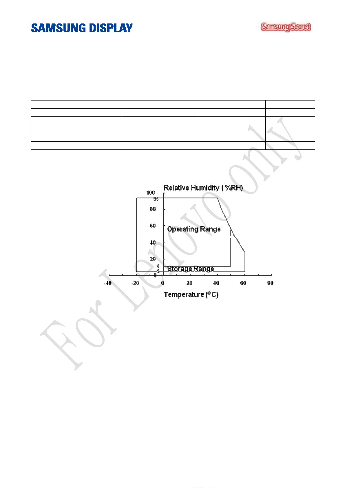
Note (1) The range of temperature and relative humidity are shown in the graph below 95% RH Max. .
(39℃ ≥ Ta) If the temperature is higher than 40 ℃, the maximum temperature of wet–bulb shall be
less than 39℃. No condensation
TOPR 0 50 C (1)
Snop
- 240 G (2), (4)
(2) Vibrate X, Y, and Z axis in the shape of the half sine wave one time for 2ms .
(3) Vibrate the X, Y, and Z randomly within a 5 - 500 Hz range for 30min.
(4) When testing a vibration and a shock, the fixture, which holds the module to be tested shall be
hard and rigid in order for the the module not to be twisted or bent by the fixture.
——————————————————————————————————————————————––—
Doc.No. LTN156AT29-L01 Page 6 of 38 Rev.No. 05-A02-G-120911
Page 7
————————————————————————————————————————————————–
2.2 ELECTRICAL ABSOLUTE RATINGS
(1) TFT LCD MODULE
V
LCD_VCC =3.3V, V
Item Symbol Min. Max. Unit Note
Power Supply Voltage
LVDS Input Voltage
V
LCD_VCC VSS - 0.3 4.0
V
LVDS VSS - 0.3 2.0
V (1),(2)
Note (1) Within Ta (25 2 C )
(2) Permanent damage to the device may occur if exceed maximum values
.
(2) BACKLIGHT UNIT
Item Symbol Min. Max. Unit Note
BLU Supply Voltage
BLU Supply Current I
V
BL_PWR
- 0.9 A
BL_PWR
VSS - 0.3 26.5 V (1), (2)
Note (1) Within Ta (25 2 C )
(2) Permanent damage to the device may occur if exceed maximum values
= GND = 0V
SS
VSS = GND = 0V
(1), (2)
Vin=12V
Duty 100%
2.3 THE OTHERS
(1) STATIC ELECTRICITY PRESSURE RESISTANCE
Item Test Conditions Remark
CONTACT DISCHARGE 150pF, 330, 8kV, 200points, 1 time/point Operating
AIR DISCHARGE 150pF, 330, 15kV, 200points, 1 time/point Operating
——————————————————————————————————————————————––—
Doc.No. LTN156AT29-L01 Page 7 of 38 Rev.No. 05-A02-G-120911
Page 8
————————————————————————————————————————————————–
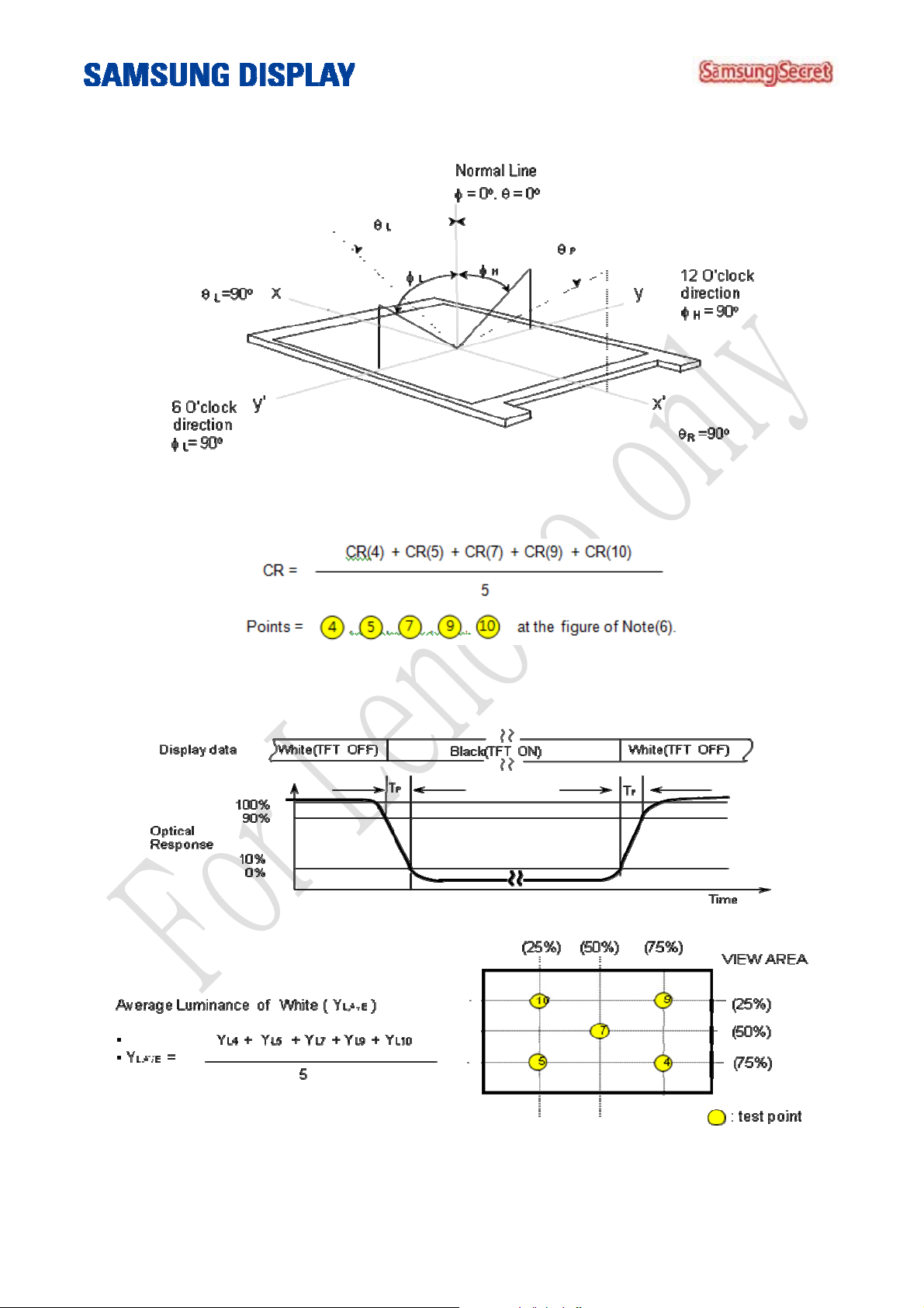
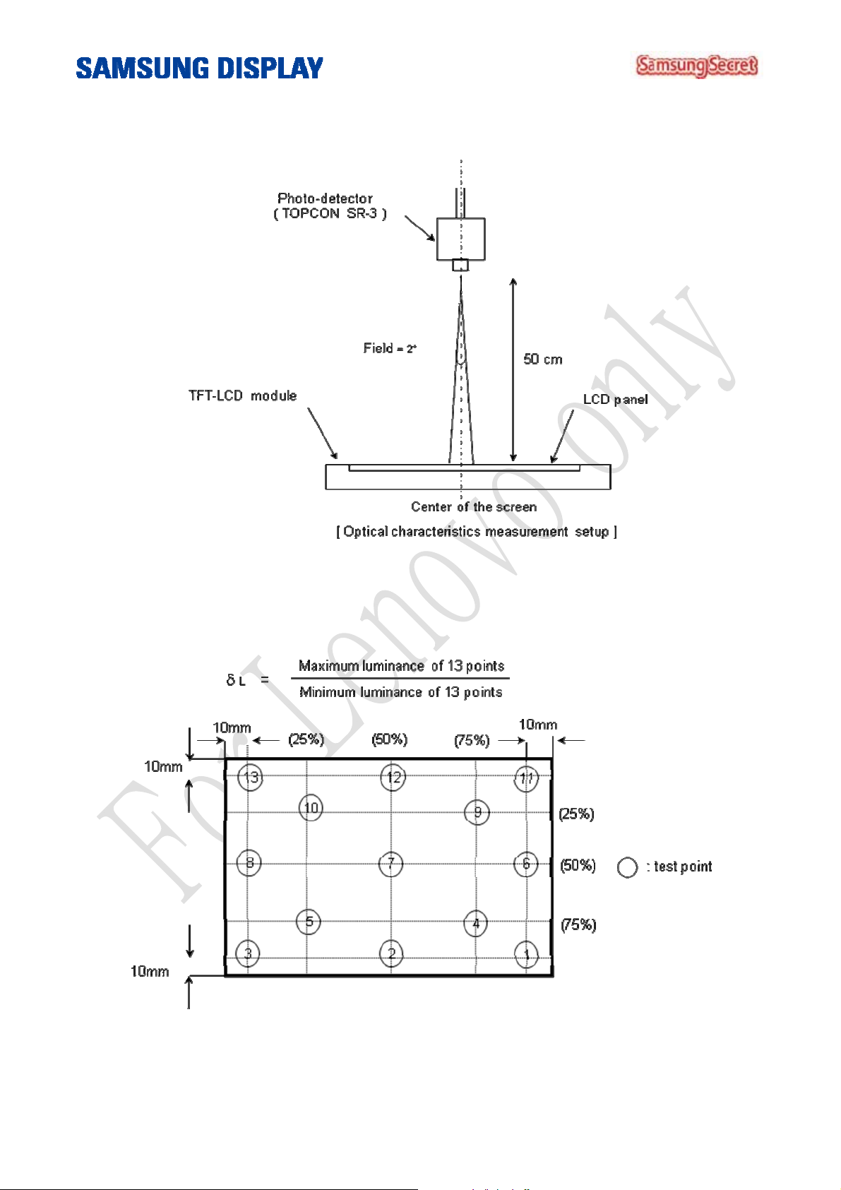
3. OPTICAL CHARACTERISTICS
The following items are measured under the stable conditions.* The optical characteristics should be measured
in the dark room or the equivalent environment by the methods shown in the Note (5).
Measuring equipment : TOPCON SR-3
Ta = 25 2 C, V
Item Symbol Condition Min. Typ. Max. Unit Note
Contrast Ratio CR
Response time
( Rising + Falling )
Average Luminance
of White (5 Points)
Red
Color
Chromaticit
Gree
n
y
(CIE)
Blue
Whit
e
Hor.
Viewing
Angle
Ver.
T
RT
Y
L,AVE
Normal
Viewing
R
X
RY
X 0.330
G
GY 0.560
X 0.160
B
Angle
= 0
= 0
BY 0.135
X 0.313
W
WY 0.329
L
H
H
CR 10
At center
L
Color
Gamut
White variation
(13P)
CG - 45 - %
L
- - 1.67 (6)
LCD_VCC =3.3V, fv= 60Hz, fDCLK = 72.33MHz, IF = 100% duty
500 - - - (1),(2),(5)
- 16 25 msec (1),(3)
IF=100%
170 200 - cd/m
2
Duty
(1),(4)
0.570
0.340
-0.03
+0.03 (1),(5)
40 45 40 45 10 20 -
Degrees (1),(5)
25 40 -
——————————————————————————————————————————————––—
Doc.No. LTN156AT29-L01 Page 8 of 38 Rev.No. 05-A02-G-120911
Page 9
————————————————————————————————————————————————–
Note (1) The definition of viewing angle : The range of viewing angle (10 C/R)
Note (2) The definition of contrast ratio (CR) : The ratio of max. gray and min gray at 5 points
(4, 5, 7, 9, and10)
Note (3) The definition of Response time : Subtotal of the time, during which the transmission changes from
10% to 90% when the TFT turns on and off.
Note (4) The definition of average luminance of white : Measure the luminance of white at 5 points.
——————————————————————————————————————————————––—
Doc.No. LTN156AT29-L01 Page 9 of 38 Rev.No. 05-A02-G-120911
Page 10
————————————————————————————————————————————————–
Note (5) Measure the panel, which is left for 30 min. at the normal temp. after leaving it for 30 min with turning
the back light on at the rating. The measurement should be executed under the condition including
the ambient temp., 25℃±2℃, the dark room, windless(removed the direct wind), and no vibration.
Note (6) The definition of white variation at 13 points ( L )
——————————————————————————————————————————————––—
Doc.No. LTN156AT29-L01 Page 10 of 38 Rev.No. 05-A02-G-120911
Page 11
————————————————————————————————————————————————–
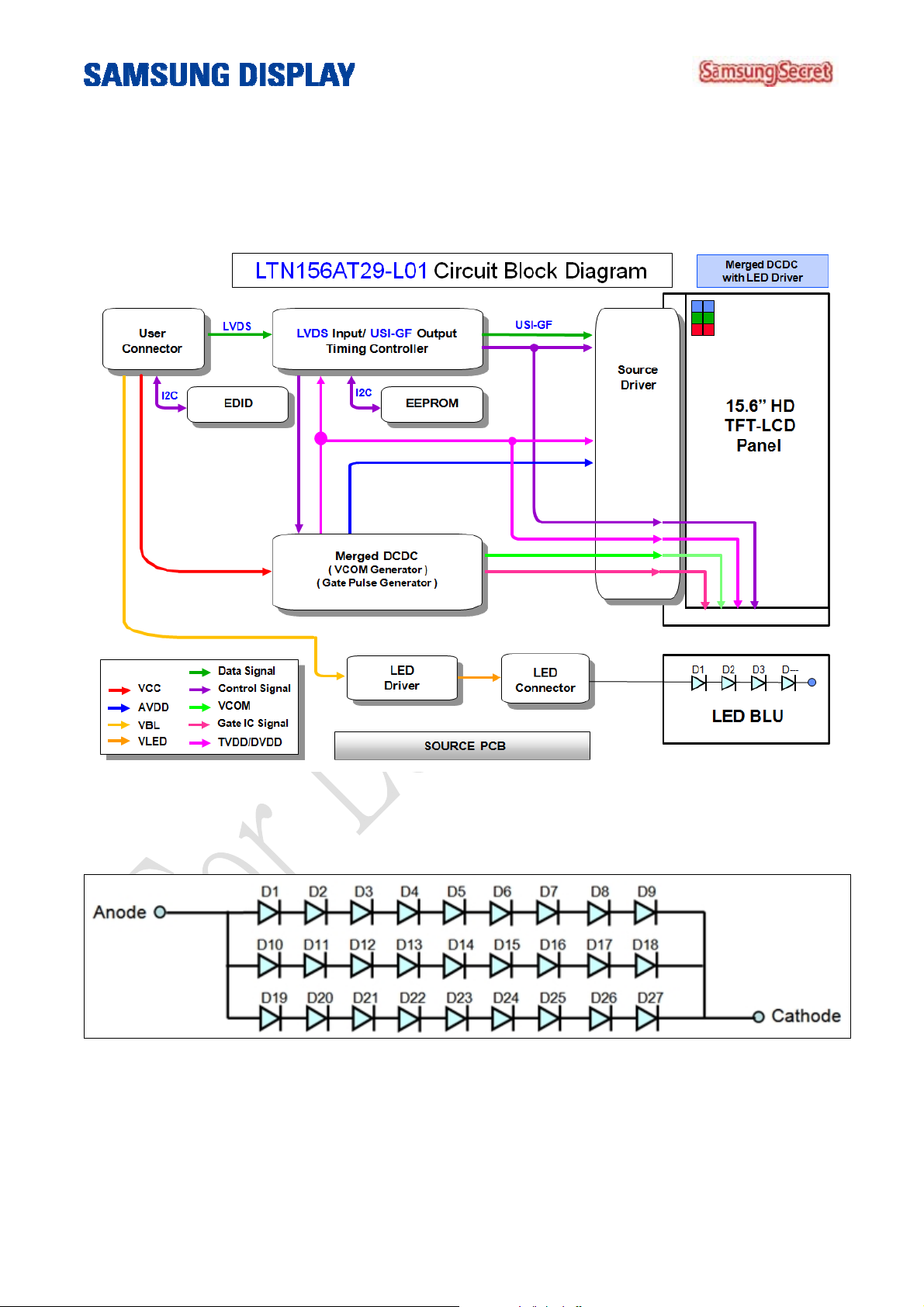
4. BLOCK DIAGRAM
4.1 TFT LCD MODULE
4.2 THE STRUCTURE OF LED PLACEMENT
( 3 channels x 9ea = 27ea )
——————————————————————————————————————————————––—
Doc.No. LTN156AT29-L01 Page 11 of 38 Rev.No. 05-A02-G-120911
Page 12
————————————————————————————————————————————————–
5. ELECTRICAL CHARACTERISTICS
5.1 TFT LCD MODULE
* Ta = 25 ± 2 °C
Item Symbol Min. Typ. Max. Unit Note
Power Supply Voltage VLCD_VCC 3.0 3.3 3.6 V
0.7
V
LCD_VCC
LCD_VCC = 3.3V , DC Current.
- - V
0.3
V
LCD_VCC
(1)
V
(2), (4)
T-CON TTL
Input Voltage
High
Low VIL - -
V
IH
60Hz fv - 60 - Hz
Vsync
50Hz fv - 50 - Hz (3)
40Hz fv - 40 - Hz (3)
Hsync 60Hz fh 46.50 47.40 48.60 kHz
60Hz fDCLK 67.24 72.33 83.88 MHz
Main Frequency
50Hz fDCLK - 60.28 - MHz
40Hz fDCLK - 48.22 - MHz
Rush Current IRUSH - - 1.5 A (5)
Input Current
White I
Mosaic ILCD_VCC - 146 - mA
Black ILCD_VCC - 145 - mA
V.Stripe
LCD_VCC - 147 - mA
ILCD_VCC - 247 450 mA
Note (1) The data pins for display and signal pins for timing should be connected.(GND= 0V)
(2) fV = 60Hz, fDCLK = 72.33 MHZ, V
(3) In the case of 40Hz & 50Hz for sDRRS, FOS, Flicker & Brightness are not guaranteed, because their
level might be different from 60Hz operation.
——————————————————————————————————————————————––—
Doc.No. LTN156AT29-L01 Page 12 of 38 Rev.No. 05-A02-G-120911
Page 13

————————————————————————————————————————————————–
Note (4) The dissipation pattern for power
Note (5) The condition for measurement for rush current
——————————————————————————————————————————————––—
Doc.No. LTN156AT29-L01 Page 13 of 38 Rev.No. 05-A02-G-120911
Page 14

————————————————————————————————————————————————–
5.2 BACK LIGHT UNIT
Ta = 25 2 C
Item Symbol Min. Typ. Max. Unit Note
LED Forward Current IF - 25 - mA
LED Forward Voltage VF 3.0 3.2 3.4 V IF = 25mA
LED Array Voltage VP - 28.8 - V VF * LED Counts
LED Power Consumption P - - 2.7 W
LED Life time Hr 12,000 - - Hour (1)
LED Counts Q - 27 - EA
Note (1) The life time (Hr) of LEDs can be defined as the time during which it continues to operate under the
condition, which the Ta is 25 2 C and IF= 25.0 mArms until the one of the following events
occurs when the brightness becomes 50% or lower than the original..
5.3 LED DRIVER
The manufacturer of LED driver: Richtek RT8510 Ta= 25 2 C
Item Symbol Min. Typ. Max. Unit Note
Input Voltage
V
BL_PWR
Input Current IBL_PWR - - 225 mA Vin=12V Duty 100%
PWM duty Ratio
External PWM Frequency
In-Rush Current
DBL_PWM_DIM
F
BL_PWM_DIM
I
RUSH_BL_PWR
5 12 21 V
0.2 - 100
PWM : 120Hz~500Hz
0.4 - 100 PWM : 500Hz~1kHz
0.8 - 100 PWM : 1kHz~2kHz
1.5 - 100 PWM : 2kHz~5kHz
%
3 - 100 PWM : 5kHz~10kHz
10 - 100 PWM : 10kHz~30kHz
0.12 1 30 kHz
- - 1.5 A (1)
——————————————————————————————————————————————––—
Doc.No. LTN156AT29-L01 Page 14 of 38 Rev.No. 05-A02-G-120911
Page 15

————————————————————————————————————————————————–
Note (1) Rush current measurement condition
——————————————————————————————————————————————––—
Doc.No. LTN156AT29-L01 Page 15 of 38 Rev.No. 05-A02-G-120911
Page 16

————————————————————————————————————————————————–
5.4 LVDS INTERFACE
LVDS DC Specifications
Characteristics Symbol Min. Typ. Max. Unit Conditions
Differential input high
threshold voltage
Differential input low
threshold voltage
Differential input voltage |VID| 200 400 600 mV
Common mode voltage VCM 0.4 1.2 1.8 V |VID|= 200mV
LVDS AC Specifications
Characteristics Symbol Min. Typ. Max. Unit Remarks
ROUTCLK frequency fRCP 67.24 72.33 83.88 Mhz
LVDS RX Skew
85MHz
(Strobe) Right
Margin
LVDS RX Skew
50MHz - - 700 ps
85MHz
(Strobe) Left
Margin
50MHz -700 - - ps
- - +200 mV
V
TH
V
-200 - - mV
TL
- - 400 ps
T
RSRM
-400 - - ps
T
RSLM
V
CM
= 1.2V
RINCLKP
RINCLKN
RIN1P
RIN1N
RIN1P-RIN1N
Tr
Vid
1 1 0 1 0 1 0
V
TH
V
TL
Vcm
0
< The definition of LVDS DC characteristics >
< The definition of LVDS Receiver Skew (Strobe) Margin >
——————————————————————————————————————————————––—
Doc.No. LTN156AT29-L01 Page 16 of 38 Rev.No. 05-A02-G-120911
Page 17

————————————————————————————————————————————————–
LVDS SSC Specification
Characteristics Symbol Min. Typ. Max. Unit Remarks
Modulation Rate Fmr -3 0 +3 %
Modulation Frequency Fmf
30
- 300 kHz
@ MAINCLK =
72.33MHz
< Definition of SSC (Spread Spectrum Clock) >
Timing diagrams of LVDS transmission
——————————————————————————————————————————————––—
Doc.No. LTN156AT29-L01 Page 17 of 38 Rev.No. 05-A02-G-120911
Page 18

————————————————————————————————————————————————–
5.5 INTERFACE TIMING
5.5.1 TIMING PARAMETERS
Signal Item Symbol Min. Typ. Max. Unit Note
Frame Frequency Cycle TV 775 790 810 Lines
Vertical active
in the display term
Scanning time in
one line
Horizontal active
in the display term
Display Period
Cycle T
Display Period T
T
- 768 - Lines
VD
1446 1526 1726 Clocks
H
- 1366 - Clocks
HD
5.5.2 TIMING DIAGRAMS OF INTERFACE SIGNAL
——————————————————————————————————————————————––—
Doc.No. LTN156AT29-L01 Page 18 of 38 Rev.No. 05-A02-G-120911
Page 19

————————————————————————————————————————————————–
5.6 INPUT COLOR DATA MAPPING
Note (1) Definition of gray : Rn: Red gray, Gn: Green gray, Bn: Blue gray (n=gray level)
Note (2) Input signal: 0 =Low level voltage, 1=High level voltage
——————————————————————————————————————————————––—
Doc.No. LTN156AT29-L01 Page 19 of 38 Rev.No. 05-A02-G-120911
Page 20

————————————————————————————————————————————————–
5.7 POWER ON/OFF SEQUENCE
To prevent the product from being latched up or the DC in the LCD module from starting an operation, the
order to turn the power on and off should be changed to the order as shown in the diagram below.
Timing (ms) Remarks
0.5<T1≤10
0<T2 ≤50
0<T3 ≤50
VLCD_VCC rising time from 10% to 90%
Interval from VLCD_VCC to valid data at power ON
Interval from valid data OFF to VLCD_VCC OFF at power Off
150≤T4 VLCD_VCC OFF time for Windows restart
200 ≤T5 Interval from valid data to B/L enable at power ON
200 ≤T6 Interval from valid data off to B/L disable at power Off
0<T7 ≤10
10<T8
10<T9
0.5<T10≤10
0.5<T11≤10
0<T12
0<T13
VLCD_VCC falling time from 90% to 10%
Interval from valid data on to LED driver Vin rising time 10%
Interval from LED driver Vin falling time 10% to valid data Off
LED V
LED V
rising time from 10% to 90%
in
falling time from 90% to 10%
in
Interval from LED driver Vin rising time 90% to PWM ON
Interval from PWM Off to LED driver Vin falling time 90%
0 ≤ T14 Interval from PWM ON to B/L Enable ON
0 ≤ T15 Interval from B/L Enable Off to PWM Off
——————————————————————————————————————————————––—
Doc.No. LTN156AT29-L01 Page 20 of 38 Rev.No. 05-A02-G-120911
Page 21

————————————————————————————————————————————————–
The backlight may be flashed if the interface signal remains floated when the above-mentioned signal
becomes invalid.
Note (1) The power voltage from system shall be supplied to the input pin of LCD constantly.
(2) Enable the voltage to the LED within the range, which the LCD is operated. The screen becomes
white when turning the back-light on before the LCD is operated or turning the LCD off before
turning the back-light off. Operation or the LCD turns off before the back-light turns off, the display
may momentarily become white.
(3) Don’t leave the system at a high impedance state, which the interface signal is out for a long time
after the Vcc is enabled.
(4) The T4 should be measured the module is fully discharged.
(5) The interface signal shall not maintain the high impedance when the power is on.
——————————————————————————————————————————————––—
Doc.No. LTN156AT29-L01 Page 21 of 38 Rev.No. 05-A02-G-120911
Page 22

————————————————————————————————————————————————–
5.8 INPUT TERMINAL PIN ASSIGNMENT
5.8.1 INPUT SIGNAL & POWER
(LVDS, Connector : 20455-040E-0 , I-PEX or the equipment with the equivalent capability)
Pin Symbol Function
1
2
3
4
5
6
7
8
9
10
11
12
13
14
15
16
17
18
19
20
21
22
23
24
25
26
27
28
29
30
31
32
33
34
35
36
37 NC APS on/off or No connection (optional)
38
39
40
NC Hot Plug Detect or No connection (optional)
LCD_VCC LCD logic and driver IC Power(3.3V typ.)
LCD_VCC LCD logic and driver IC Power(3.3V typ.)
VCC_EDID DDC power
NC (WPN) Reserved for the use by LCD manufacturer (WPN)
CLK_EDID DDC clock
DAT_EDID DDC data
RX0- Negative LVDS differential data input for pixel
RX0+ Positive LVDS differential data input for pixel
H_GND High speed ground
RX1- Negative LVDS differential data input for pixel
RX1+ Positive LVDS differential data input for pixel
H_GND High speed ground
RX2- Negative LVDS differential data input for pixel
RX2+ Positive LVDS differential data input for pixel
H_GND High speed ground
RXC- Negative LVDS differential clock input for pixel
RXC+ Positive LVDS differential clock input for pixel
LCD_GND LCD logic and driver IC Ground
NC No connection
NC No connection
LCD_GND LCD logic and driver IC Ground
NC No connection
NC No connection
LCD_GND LCD logic and driver IC Ground
NC No connection
NC No connection
LCD_GND LCD logic and driver IC Ground
NC No connection
NC No connection
BL_GND Backlight ground
BL_GND Backlight ground
BL_GND Backlight ground
NC Hot Plug Detect or No connection (optional)
BL_PWM_DIM Signal input for the system PWM for dimming
BL_ENABLE Backlight on/off
BL_PWR Backlight power
BL_PWR Backlight power
BL_PWR Backlight power
——————————————————————————————————————————————––—
Doc.No. LTN156AT29-L01 Page 22 of 38 Rev.No. 05-A02-G-120911
Page 23

————————————————————————————————————————————————–
6. PIXEL FORMAT
1366
Line 768
——————————————————————————————————————————————––—
Doc.No. LTN156AT29-L01 Page 23 of 38 Rev.No. 05-A02-G-120911
Page 24

————————————————————————————————————————————————–
7. OUTLINE DIMENSION
[Refer to next page]
——————————————————————————————————————————————––—
Doc.No. LTN156AT29-L01 Page 24 of 38 Rev.No. 05-A02-G-120911
Page 25

ڊ
ڋڌ
ڧگکڌڐڑڜگڍڔڈڧڋڌ
کڜڨڠ
ګڜڭگڊڮڣڠڠگ
ڮګڠڞډٻکڪ
ڟڠڮڞڭڤګگڤڪکٻڪڡٻڭڠڱڤڮڤڪک
ڟڭڜڂکٻڝڴ ڟڠڮڂڟٻڝڴ ڞڣڦڂڟٻڝڴ ڜګګڂڟٻڝڴ
ۈۈ
ڟڜگڠ
ڧڠڱڠڧٻڎ
ڰکڤگ
ڮڞڜڧڠ ڊ
ڭڠڱ
ڢڠکڠڭڜڧٻگڪڧڠڭڜکڞڠ
ڮگڠګ ڧڠڱڠڧٻڌ ڧڠڱڠڧٻڍ ڧڠڱڠڧٻڎ
ڧگکڌڐڑڜگڍڔ
ڰڮ
ڨڜڟڠٻڤکٻڞڣڤکڜ
ڞ
ڟ ಕ
ͽ΅ͿͲ΅ͽΆ΅ͽͺͿͶ
ڤڪک
ڡڤڧڠٻکڪډ
ڭڠڱڤڮ
Page 26

————————————————————————————————————————————————–
8. RELIABILITY TEST
Item Condition Time/Cycle
HTOL
LTOL
HTS
LTS
THB
WHTS
T/C
operating
ESD
Operating
Box Vibration
(Non-operating)
Shock
(Non-operating)
Non-
55 ℃
-5 ℃
70 ℃
-25 ℃
50 ℃, 90%
60 ℃, 75%
-40 ℃/30min ~ 65 ℃/30min
CDM : 150pF, 330Ω, 9point, 3 times/point ±10kV
Contact : 150 pF, 330Ω, 100point, once/point ±8kV
Air(non-contact) : 150pF, 330Ω, 100point, once/point ±15kV
5~200Hz, 1.05Grms, 2hr/Y 1time
240G, 2msec, ±XYZ 30min/axis
500 hrs
500 hrs
500 hrs
500 hrs
500 hrs
500 hrs
50 cycles
HINGE 10~170˚, Open/Close 2sec, Pause1sec 30Kcycle
Altitude -40~50℃, 0~45,000ft 72.5Hr
[Result Evaluation Criteria ]
Under the display quality test conditions with normal operation state,
these should be no change which may affect practical display functions.
——————————————————————————————————————————————––—
Doc.No. LTN156AT29-L01 Page 26 of 38 Rev.No. 05-A02-G-120911
Page 27

————————————————————————————————————————————————–
9. PACKING
9.1 CARTON
(1) Packing Form
Corrugated Cardboard box and Corrupad form as shock absorber.
(2) Packing Method
Note (1) Total Weight : Approximately 18 Kg
(2) Acceptance number of piling : 36 sets
(3) Carton size : 373(W) 470(D) 372(H))
(3) Packing Material
No Part name Quantity
1 Static electric protective sack 36 pcs
2 Packing case (Inner box)
included shock absorber
3 Pictorial marking 2
4 Carton 1 set
——————————————————————————————————————————————––—
1 set
Doc.No. LTN156AT29-L01 Page 27 of 38 Rev.No. 05-A02-G-120911
Page 28

————————————————————————————————————————————————–
9.2 MARKING
A nameplate is affixed to the specified location on each product.
(1)Parts number : LTN156AT29-L01
(2)Revision code : 3 letters
(3)Lot number : X X X X XXX XX X L01
Samsung Revision Code
Panel number
Cell ID
Lot ID
Month
Year
Product Code
Line
(4) Nameplate Indication
D
1225
MADE IN CHINA
Parts name : LTN156AT29 –L01
Lot number : XXXXXXXXXX
Inspected work week : 1225 (2012 year 25th week)
Product Revision Code : L01
LTN156AT29
XXXXXXXXXX L01
80 mm
40 mm
——————————————————————————————————————————————––—
Doc.No. LTN156AT29-L01 Page 28 of 38 Rev.No. 05-A02-G-120911
Page 29

————————————————————————————————————————————————–
(5) Packing small box attach
D
DEVICE : LTN156AT29
TYPE : L01
QUANTITY : 36 PCS
MADE IN CHINA
XXXXXXXXXX
——————————————————————————————————————————————––—
Doc.No. LTN156AT29-L01 Page 29 of 38 Rev.No. 05-A02-G-120911
Page 30

————————————————————————————————————————————————–
10. GENERAL PRECAUTIONS
10.1 HANDLING
(a) When the module is assembled, It should be attached to the system firmly using every mounting holes.
Be careful not to twist and bend the modules.
(b) Refrain from strong mechanical shock and / or any force to the module. In addition to damage, this may
cause improper operation or damage to the module and CCFT back-light.
(c) Note that polarizers are very fragile and could be easily damaged. Do not press or scratch the surface
harder than a HB pencil lead.
(d) Wipe off water droplets or oil immediately. If you leave the droplets for a long time, Staining and
discoloration may occur.
(e) If the surface of the polarizer is dirty, clean it using some absorbent cotton or soft cloth.
(f) The desirable cleaners are water, IPA (Isoprophyl Alcohol) or Hexane. Do not use Ketone type materials(ex.
Acetone), Ethyl alcohol, Toluene, Ethyl acid or Methyl chloride. It might permanent damage to the polarizer
due to chemical reaction.
(g) If the liquid crystal material leaks from the panel, it should be kept away from the eyes or mouth .In case
of contact with hands, legs or clothes, it must be washed away thoroughly with soap.
(h) Protect the module from static , it may cause damage to the C-MOS Gate Array IC.
(i) Use fingerstalls with soft gloves in order to keep display clean during the incoming inspection and assembly
process.
(j) Do not disassemble the module.
(k) Do not pull or fold the LED FPC.
(l) Do not touch any component which is located on the back side.
(m) Protection film for polarizer on the module shall be slowly peeled off just before use so that the
electrostatic charge can be minimized.
(n) Pins of I/F connector shall not be touched directly with bare hands.
——————————————————————————————————————————————––—
Doc.No. LTN156AT29-L01 Page 30 of 38 Rev.No. 05-A02-G-120911
Page 31

————————————————————————————————————————————————–
10.2 STORAGE
We highly recommend to comply with the criteria in the table below.
ITEM Unit Min. Max.
Storage
Temperature
Storage
Humidity
Storage Life 12 months
Storage
Condition
- The storage room should be equipped with a good ventilation facility, which has a
temperature controlling system.
- Products should be placed on the pallet, which is away from the wall not on the floor.
- Prevent products from being exposed to the direct sunlight, moisture, and water.;
Be cautious not to pile the products up.
- Avoid storing products in the environment, which other hazardous material is placed.
- If products are delivered or kept in the storage facility more than 3 months,we recommend
you to leave products under the condition including a 20℃ temperature and a humidity of
50% for 24 hours.
- If you store semi-manufactured products for more than 3 months, bake the products under
the condition including the 50℃ temp. and the 10% humidity for 24hrs after being used.
(℃) 5 40
(%rH) 35 75
10.3 OPERATION
(a) Do not connect, disconnect the module in the “ Power On” condition.
(b) Power supply should always be turned on/off by following item 6.3 “ Power on/off sequence “.
(c) Module has high frequency circuits. Sufficient suppression to the electromagnetic interference shall be
done by system manufacturers. Grounding and shielding methods may be important to minimize the
interference.
(d) The FPC cable between the LED chips and its converter power supply shall be a minimized length and be
connected directly .The longer cable between the back-light and the converter may cause lower luminance
of light source (LED).
(e) The standard limited warranty is only applicable when the module is used for general notebook
applications. If used for purposes other than as specified, SEC is not to be held reliable for the defective
operations. It is strongly recommended to contact SEC to find out fitness for a particular purpose.
——————————————————————————————————————————————––—
Doc.No. LTN156AT29-L01 Page 31 of 38 Rev.No. 05-A02-G-120911
Page 32

————————————————————————————————————————————————–
10.4 OTHERS
(a) Ultra-violet ray filter is necessary for outdoor operation.
(b) Avoid condensation of water. It may result in improper operation or disconnection of electrode.
(c) Do not exceed the absolute maximum rating value. ( the supply voltage variation, input voltage variation,
Variation in part contents and environmental temperature, so on) Otherwise the module may be damaged.
(d) If the module displays the same pattern continuously for a long period of time, it can be the situation when
The image “sticks” to the screen.
(e) This module has its circuitry PCB’s on the rear side and should be handled carefully in order not to be
stressed.
——————————————————————————————————————————————––—
Doc.No. LTN156AT29-L01 Page 32 of 38 Rev.No. 05-A02-G-120911
Page 33

————————————————————————————————————————————————–
11. EDID
Address Value ASCII
FUNCTION BIN
(HEX) HEX Data
00 00 00000000 0
01 FF 11111111 255
02 FF 11111111 255
03 FF 11111111 255
04 FF 11111111 255
05 FF 11111111 255
06 FF 11111111 255
07 00 00000000 0
08 4C 01001100 76 S
09 83 10000011 131 C
0A 52 01010010 82 [R]
0B 45 01000101 69 [E]
0C 00 00000000 0
0D 00 00000000 0
0E 00 00000000 0
0F 00 00000000 0
10 Week o f manufac ture 00 00000000 0
11 Y ear of manufact ure 16 00010110 22 2012
12 EDID Structure Ver . 01 00000001 1 1
13 EDID revision # 03 00000011 3 3
14 V ideo input definition 80 10000000 128
15 M ax H image size 22 00100010 34 34
16 M ax V image size 13 00010011 19 19
17 Display Gamma 78 01111000 120 2.2
18 Featur e support 0A 00001010 10
19 Red/green low bit s 09 00001001 9
1A Blue/white low bits 25 00100101 37
1B Red x/ high bits 92 10010010
1C Red y 57 01010111
1D Green x 54 01010100
1E Gr een y 8F 10001111
1F Blue x 29 00101001
20 Blue y 22 00100010
21 White x
22 White y 54 01010100
23 Established timing 1 00 00000000 0
24 Established timing 2 00 00000000 0
25 Established timing 3 00 00000000 0
26 01 00000001 1
27 01 00000001 1
28 01 00000001 1
29 01 00000001 1
Header
ID Manufacturer Name
ID Product Code
32-bit serial no.
50 01010000
Standar d t iming #1
Standar d t iming #2
DEC Notes
146
87
84
143
41
34
80
84
or
D
0.570
0.340
0.330
0.560
0.160
0.135
0.313
0.329
EDID Header
3 character I D
"SDC"
2012
EDID Ver. 1.0
EDID Rev . 3
34 cm(approx)
19 cm(approx)
Gamma 2.2
10000111
11111110
Red x 0.570=
10010010
Red y 0.340=
01010111
Green x 0.330=
01010100
Green y 0.560=
10001111
Blue x 0.160=
00101001
Blue y 0.135=
00100010
Whit e x 0.313=
01010000
Whit e y 0.329=
01010100
not used
not used
——————————————————————————————————————————————––—
Doc.No. LTN156AT29-L01 Page 33 of 38 Rev.No. 05-A02-G-120911
Page 34

————————————————————————————————————————————————–
t
t
2A 01 00000001 1
2B 01 00000001 1
2C 01 00000001 1
2D 01 00000001 1
2E 01 00000001 1
2F 01 00000001 1
30 01 00000001 1
31 01 00000001 1
32 01 00000001 1
33 01 00000001 1
34 01 00000001 1
35 01 00000001 1
36 41 01000001 65 72.33
37 1C 00011100 28
38 56 01010110 86 1366
39 A0 10100000 160 160
3A 50 01010000 80
3B 00 00000000 0 768
3C 16 0001 0110 22 22
3D 30 0011 0000 48
3E 30 00110000 48 48
3F 20 00100000 32 32
40
Standar d t iming #3
Standar d t iming #4 not used
Standar d t iming #5
Standar d t iming #6
Standar d t iming #7
Standar d t iming #8
Detailed timing/monitor
descriptor #1
25 00100101 37
2
5
not used
not used
not used
not used
not used
M ain c lock = 72.33 MHz
Hor act ive=1366 pixels
Hor blanking=160 pixels
4bit : 4bi
V er tcal active=768 lines
Vert ic al blanking= 22 lines
4bit : 4bi
Hor sync . Offset= 48 pixels
H sync. W idth=32 pixels
V sync . O ffset= 2 lines
V sync. Width= 5 lines
41 00 00000000 0
42 58 01011000 88 344
43 C2 1 1000010 194 194
44 10 00010000 16
45 00 00000000 0
46 00 00000000 0
47 19 00011001 25
48 00 00000000 0
49 00 00000000 0
4A 00 00000000 0
4B 0F 0000 1111 15
4C 00 0000 0000 0
4D 00 0000 0000
4E 00 00000000
4F 00 00000000
50 00 00000000
51 00 00000000
52 00 00000000
53 00 00000000
54 00 00000000
55 1E 00011110
56 B4 10110100
57 02 00000010
58 74 01110100
59 00 00000000 0
Detailed timing/monitor
descriptor #2
0
0
0
0
0
0
0
0
30
180
2
116
2bit : 2bit :2bit :2bit
H image size= 344 mm(approx )
V image size = 194 mm(approx)
No Horizontal B or der
No Vertical Border
M anufact ur er S pecified (T iming)
=HSPWmin / 2
Value
=HSPWmax / 2
Value
=Thbpmin /2
Value
=Thbpmax /2
Value
=V SPW min /2
Value
=V SPW max /2
Value
=Tvbpmin / 2
Value
=Tvbpmax / 2
Value
Thpmin=
Thpmax=
Tvpmin=
Tvpmax=
Module revision
*2 + HA pixelclks
value
*2 + HA pixelclk s
value
*2 + VA lines
value
*2 + VA lines
value
——————————————————————————————————————————————––—
Doc.No. LTN156AT29-L01 Page 34 of 38 Rev.No. 05-A02-G-120911
Page 35

————————————————————————————————————————————————–
5A 00 00000000 0
5B 00 00000000 0
5C 00 0000 0000 0
5D FE 11111110 254
5E 00 00000000 0
5F 53 01010011 83 [S]
60 41 01000001 65 [A]
61 4D 01001101 77 [M]
62 53 01010011 83 [S]
63 55 01010101 85 [U]
64 4E 01001110 78 [N]
65 47 01000111 71 [G]
66 0A 00001010 10 [^]
67 20 00100000 32 [ ]
68 4C 01001100 76
69 83 10000011 131
6A 41 01000001 65 [A]
6B 54 01010100 84 [T]
6C 00 0000 0000 0
6D 00 0000 0000 0
6E 00 00000000 0
6F FE 11111110 254
70 00 00000000 0
71 4C 01001100 76 [L]
72 54 01010100 84 [T]
73 4E 01001110 78 [N]
74 31 00110001 49 [1]
75 35 00110101 53 [5]
76 36 00110110 54 [6]
77 41 01000001 65 [A]
78 54 01010100 84 [T]
79 32 00110010 50 [2]
7A 39 00111001 57 [9]
7B 4C 01001100 76 [L]
7C 30 0011 0000 48 [0]
7D 31 0011 0001 49 [1]
7E Ext ension Flag 00 00000000 0
7F Checksum
Detailed timing/monitor
descriptor #3
Detailed timing/monitor
descriptor #4
7F
01111111
127
A S CII Data St r ing Tag
supplier ID "SDC"
Product code "AT"
(Hex, LSB first)
Monitor Name Tag (ASCII)
——————————————————————————————————————————————––—
Doc.No. LTN156AT29-L01 Page 35 of 38 Rev.No. 05-A02-G-120911
Page 36

————————————————————————————————————————————————–
12. APPENDIX
12.1 SYSTEM DESIGN GUIDE
[Common]Gap in the rear of display
1
Recommendation
Risk factor Pooling / White Spot / Being divided
2
Prevent the product from being defected resulted from the interference and the lack
of gap between the rear cover of system and the LCD module.
A. The gap between the rear cover of system and the rear of LCD module : Min.
1.0mm
B. Based on the size of part in a maximum size between the rear cover of system and
the LCD module. : Min. 1.0mm
(※ Based on the maximum thickness of module, which the tolerance is considered.)
[Common] The shape of key pad of system
Prevent the product from being defected resulted from the shape of key pad in the
system.
A. Make the shape of frame, which surrounds the key pad as round as possible.
B. Prevent the product from being defected resulted from the pressurization by
Recommendation
Risk factor White Spot / Black Spot / Being broken in glass.
——————————————————————————————————————————————––—
attaching the sponge on the cover of system not to be overlapped with the
position of the frame around key pad.
C. Prevent the product from being defected, which is resulted from the
pressurization from outside by eliminating the difference in height between the key
pad and the frame around key pad.
Doc.No. LTN156AT29-L01 Page 36 of 38 Rev.No. 05-A02-G-120911
Page 37

————————————————————————————————————————————————–
[Common] The arrangement of user cable (Camera, Antenna)
3
Prevent the product from being defected resulted from the user cable arranged
on the rear of module.
Recommendation
Risk factor Pooling / White Spot
4
Recommendation
Risk factor A/D (The damaged COF film is cracked., The chip is broken.)
5
A. Arrange the user cable in the side not in the rear(the active area) of
LCD module.
[Common] The arrangement of input cable
Prevent the product from being defected resulted from the overlapping
between the input cable and the film of LCD module .
A. Arrange the input cable not to be overlapped with the COF film.
B. Minimization of the height of input cable and making the COF film flat.
[ELS] Gap between the bracket and the LCD Module
Prevent the LCD module from being interfered when testing the product in
terms of the performance of hinge and the occurrence of twist.
A. Secure the min. 1.0mm distance between the bracket and the LCD module at
Recommendation
——————————————————————————————————————————————––—
4 corners of screen respectively.
B. Control the angle of bracket on the system.
Doc.No. LTN156AT29-L01 Page 37 of 38 Rev.No. 05-A02-G-120911
Page 38

————————————————————————————————————————————————–
[ELS] Suggestion on the angle of bracket
6
Prevent the product from being defected resulted from the changed top chassis
by the angle and the shape of bracket on the system.
A. Don't form the bracket hole.
Recommendation
Risk factor Pooling / Light leakage
7
B. Control the angle in the event that the bracket, which has L-shape is applied.
(90 ± 2˚)
[UMS] Control the angle of the connected part on the user flange
Prevent the user flange from not being placed horizontally, which is caused
when the LCD module, which is structured in UMS is assembled.
A. Prevent the product from being pooled resulted from the changed user
flange
Recommendation
Risk factor Pooling
created when assembling the LCD module to the system.
B. Insert the screw to the hole of flange vertically when LCD module is
assembled to the system.
——————————————————————————————————————————————––—
Doc.No. LTN156AT29-L01 Page 38 of 38 Rev.No. 05-A02-G-120911
 Loading...