

Samsung LTM190EP01 Datasheet
ISSUED DATE : 2008-01-14
PRODUCT INFORMATION
PRODUCT INFORMATION
SAMSUNG TFT--
SAMSUNG TFT
SAMSUNG TFT-LCD PRODUCT INFORMATION
MODEL
MODEL
MODEL : LTM190EP01
www.jxlcd.com
www.jxlcd.com
LCD PRODUCT INFORMATION
LCD PRODUCT INFORMATION
: LTM190EP01
: LTM190EP01
Note : This is Product Information is subject to change after 3 months of issuing date.
LCD Development Team 4
Samsung Electronics Co . , LTD.
000_G_080114Doc No 1/34PageLTM190EP01MODEL
PRODUCT INFORMATION
PRODUCT INFORMATION
Contents
General Description --------------------------------------------------------------------------------- (3)
1. Absolute Maximum Ratings ------------------------------------------------------------------- (4)
2. Optical Characteristics --------------------------------------------------------------------------- (6)
3. Electrical Characteristics ---------------------------------------------------------------------- (11)
3.1 TFT LCD Module
3.2 Back Light Unit
4. Block Diagram ----------------------------------------------------------------------------------- (16)
4.1 TFT LCD Module
4.2 Back Light Unit
5. Input Terminal Pin Assignment -------------------------------------------------------------- (17)
5.1 Input Signal & Power
5.2 LVDS Interface
5.3 Back Light Unit
5.4 Input Signals, Basic Display Colors and Gray Scale of Each Color
6. Interface Timing --------------------------------------------------------------------------------- (26)
6.1 Timing Parameters (DE only mode)
6.2 Timing Diagrams of interface Signal (DE only mode)
6.3 Power ON/OFF Sequence
6.4 LVDS Input Characteristics
6.5 VDD Power Dip Condition
7. Outline Dimension ------------------------------------------------------------------------------- (30)
8. General Precaution ------------------------------------------------------------------------------ (32)
www.jxlcd.com
www.jxlcd.com
8.1 Handling
8.2 Storage
8.3 Operation
8.4 Others
000_G_080114Doc No 2/34PageLTM190EP01MODEL
PRODUCT INFORMATION
General Description
Description
LTM190EP01 is a color active matrix liquid crystal display (LCD) that uses amorphous
silicon TFT(Thin Film Transistor) as switching components. This model is composed of
a TFT LCD panel, a driver circuit and a back light unit. The resolution of a 19.0” is 1280
x 1024 and this model can display up to 16.7 millions colors.
Features
High contrast ratio, high aperture structure
PVA (Plus Viewing Angle) mode
Wide Viewing Angle
High speed response (DCC Technology)
SXGA (1280 x 1024 pixels) resolution
Low power consumption
2 dual CCFTs (Cold Cathode Fluorescent Tube)
DE (Data Enable) only mode
LVDS (Low Voltage Differential Signaling) interface (2pixel/clock)
Compact Size Design
RoHS, TCO’03 compliance
PRODUCT INFORMATION
Applications
Workstation & desktop monitors
www.jxlcd.com
Display terminals for AV application products
Monitors for industrial machine
* If the module is used to other applications besides the above, please contact SEC
in advance.
www.jxlcd.com
General Information
Haze 44% , Hard-Coating (3H)Surface Treatment
UnitSpecificationItems
mm0.294(H) x 0.294(W)Pixel Pitch
mm376.32(H) x 301.056(V)Active Display Area
colors16.7M Display Colors
pixel1280 x 1024Number of Pixels
RGB vertical stripePixel Arrangement
Note
Normally BlackDisplay Mode
cd/㎡300 (Typ.)Luminance of White
000_G_080114Doc No 3/34PageLTM190EP01MODEL
Mechanical Information
PRODUCT INFORMATION
PRODUCT INFORMATION
Module
size
Note (1) Mechanical tolerance is ± 0.5mm unless there is a special comment.
1. Absolute Maximum Ratings
Max.
396.5
324.5
17.0
2,250
NoteUnitTyp.Min.Item
mm396.0395.5Horizontal (H)
w/o inverter ass’y
Mm324.0323.5Vertical (V)
mmDepth (D)
LCD module onlygWeight
If the condition exceeds maximum ratings, it can cause malfunction or unrecoverable
damage to the device.
Glass surface temperature
Shock ( non - operating )
Vibration ( non - operating )
Note (1) Ta= 25 ± 2 °C
www.jxlcd.com
www.jxlcd.com
Power Supply Voltage
Storage temperature
(Operation)
DD
STG
OPR
nop
nop
NoteUnitMax.Min.SymbolItem
V6.5GND-0.5V
60-20T
500T
℃
℃
(1)
(2)G50-S
(3)G1.5-V
000_G_080114Doc No 4/34PageLTM190EP01MODEL
PRODUCT INFORMATION
PRODUCT INFORMATION
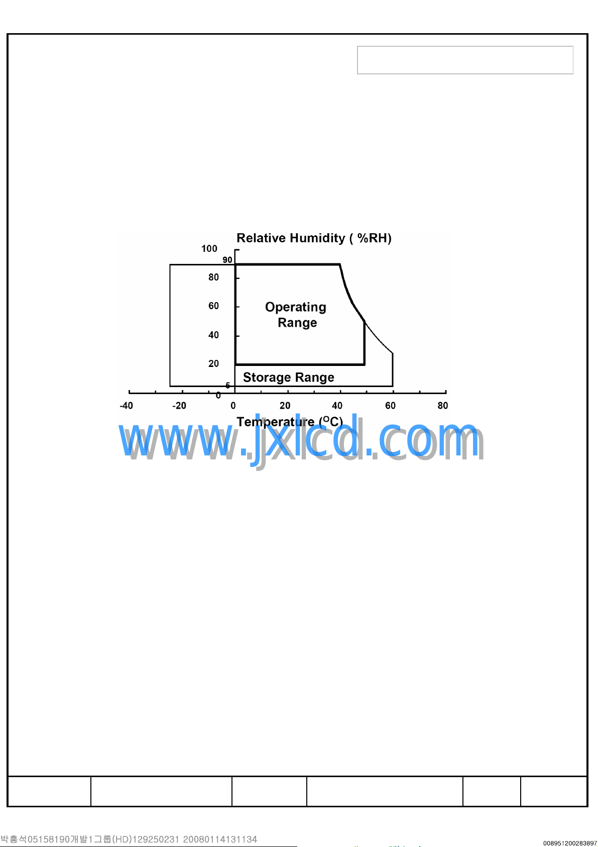
(1) Temperature and relative humidity range are shown in the figure below.
a. 90 % RH Max. (Ta ≤ 39 °C)
b. Maximum wet-bulb temperature at 39 °C or less. (Ta ≤ 39 °C)
c. No condensation
(2) 11ms, sine wave, one time for ±X, ±Y, ±Z axis
(3) 10-300 Hz, Sweep rate 10min, 30min for X,Y,Z axis
(39,90)
(39,90)
(39,90)
(39,90)
(50,50.4)
(50,50.4)
(50,50.4)
(50,50.4)
(60,27.7)
(60,27.7)
(60,27.7)
(60,27.7)
25,5)
25,5)
((--25,5)
((--25,5)
www.jxlcd.com
www.jxlcd.com
Fig. Temperature and Relative humidity range
000_G_080114Doc No 5/34PageLTM190EP01MODEL
PRODUCT INFORMATION
2. Optical Characteristics
PRODUCT INFORMATION
The optical characteristics should be measured in a dark room or equivalent.
Measuring equipment : TOPCON RD-80S,SPECTRORADIOMETER SR-3
(Ta = 25 ± 2°C, VDD=5V, fv= 60Hz, fDCLK=54MHz, IL = 6.5mArms)
NoteUnitMax.Typ.Min.ConditionSymbolItem
Contrast Ratio
(Center of screen)
Response
Time
Luminance of White
(Center of screen)
Green
Color
Chromaticity
(CIE 1931)
www.jxlcd.com
White
Color
Chromaticity
(CIE 1976)
Green
-1,5001,000C/R
128-Tg-g.avrG-to-G
L
Rx
Red
-0.030
Blue
www.jxlcd.com
Normal
θ
=0
L,R
θ
=0
U,D
Red
Blue
Viewing
Angle
0.640
0.330Ry
0.300Gx
0.600Gy
+0.030
0.150Bx
0.060By
0.313Wx
0.329Wy
-0.451-Ru'
-0.523-Rv'
-0.125-Gu'
-0.563-Gv'
-0.175-Bu'
-0.158-Bv'
msec
cd/m2-300250Y
(3)
SR-3
(5)
RD-80S
(6)
SR-3
(7),(8)
SR-3
-0.198-Wu'
White
-0.468-Wv'
C.G.L
* C.G.L : Color Grayscale Linearity (continue to the next page)
△u'v'White
(9)0.02--
000_G_080114Doc No 6/34PageLTM190EP01MODEL
PRODUCT INFORMATION
PRODUCT INFORMATION
NoteUnitMax.Typ.Min.ConditionSymbolItem
%-72--Color Gamut
K-6500--Color Temperature
θ
Hor.
Viewing
Angle
Ver.
Brightness Uniformity
(9 Points)
Note (1) Test Equipment Setup
The measurement should be executed in a stable, windless and dark room between
30min after lighting the back light at the given temperature for stabilization
of the back light. This should be measured in the center of screen.
Single lamp current : 6.5mA
Environment condition : Ta = 25 ± 2 °C
www.jxlcd.com
www.jxlcd.com
L
θ
R
θ
U
θ
D
uni
CR≥10
-8980
-8980
Degrees
-8980
-8980
%25--B
(8)
EZ-
Contrast
(4)
SR-3
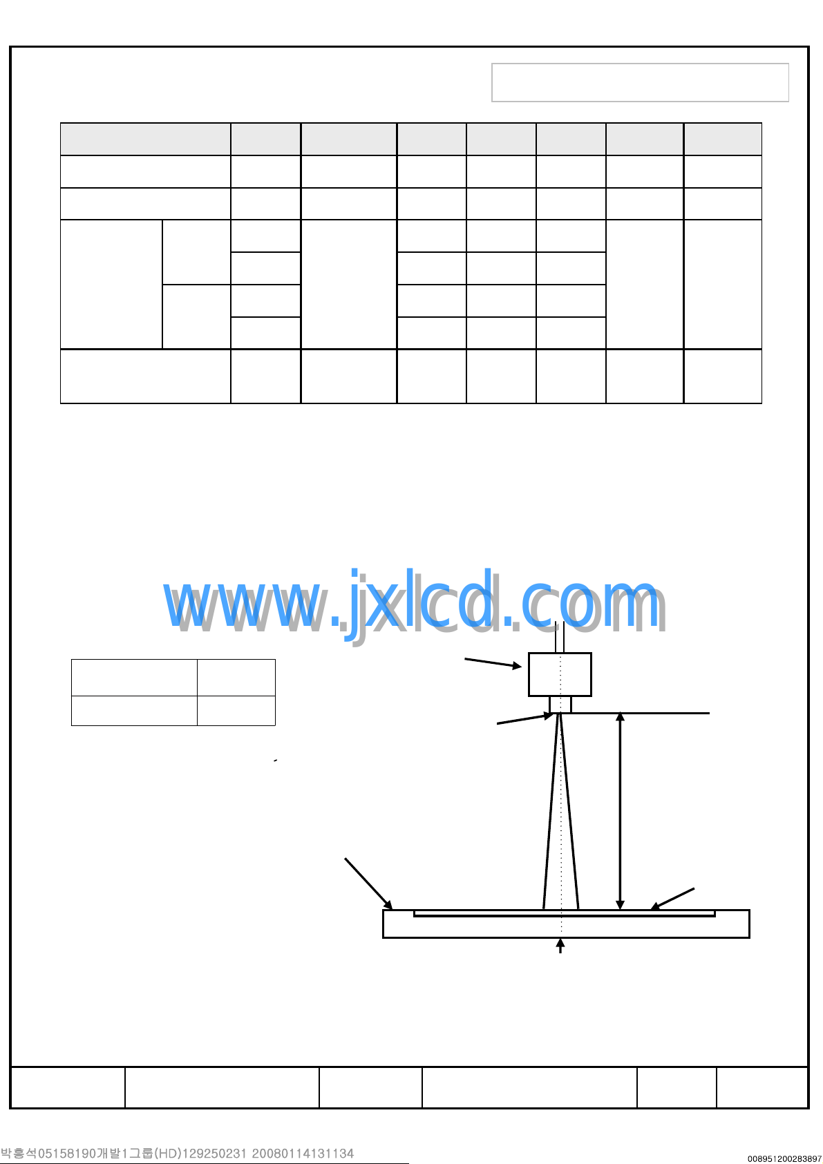
Field Photo detector
2°SR-3
TFT - LCD Module
Photo detector
Field
SR-3 : 40㎝
RD-80S : 50㎝
LCD Panel
The center of the screen
000_G_080114Doc No 7/34PageLTM190EP01MODEL
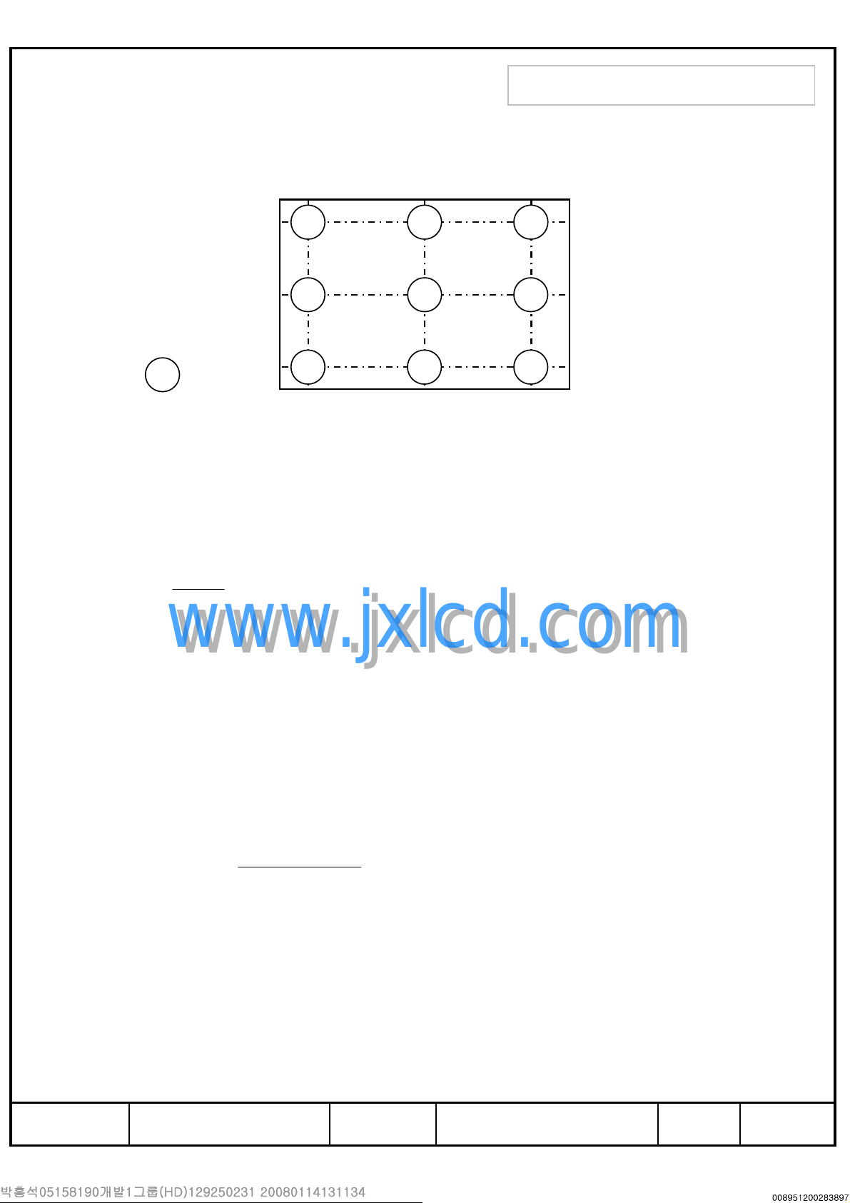
Note (2) Definition of test point
B
−
max
G
min
128 640 1152
PRODUCT INFORMATION
PRODUCT INFORMATION
Active Area
6
: Test Point
Note (3) Definition of Contrast Ratio (C/R)
: Ratio of gray max (Gmax) & gray min (Gmin) at the center point⑤ of the panel
G
CR
max
=
3 2 1
8 79
45
102
512
922
www.jxlcd.com
Gmax : Luminance with all pixels white
www.jxlcd.com
Gmin : Luminance with all pixels black
Note (4) Definition of 9 points brightness uniformity
B B
Buni
= ×
100
Bmax : Maximum brightness
Bmin : Minimum brightness
( max min)
000_G_080114Doc No 8/34PageLTM190EP01MODEL
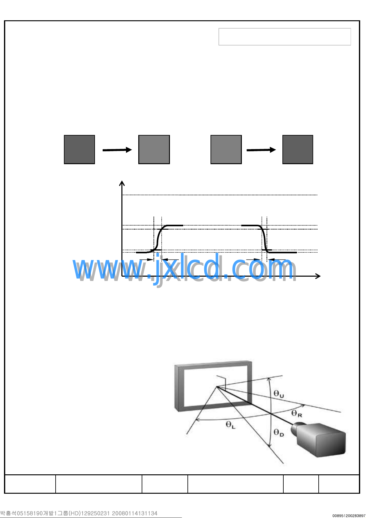
Note (5) Definition of Response time
a. Gray to Gray Response Time
- Measuring gray : 31 63, 63 95,95 127, 127 159, 159 191, 191 223
grays and vice versa
- T
G-G, avg
(Example)
: Average response time of ones between above grays
White
PRODUCT INFORMATION
PRODUCT INFORMATION
96 gray 128 gray95 gray 127 gray
100%
Gray to Gray
Response
www.jxlcd.com
www.jxlcd.com
Note (6) Definition of Luminance of White : Luminance of white at center point⑤
Note (7) Definition of Color Chromaticity (CIE 1931, CIE1976)
Color coordinate of Red, Green, Blue & White at center point⑤
Note (8) Definition of Viewing Angle
: Viewing angle range (CR ≥10)
90%
10%
0%
Black
T
r
T
f
000_G_080114Doc No 9/34PageLTM190EP01MODEL
PRODUCT INFORMATION
PRODUCT INFORMATION
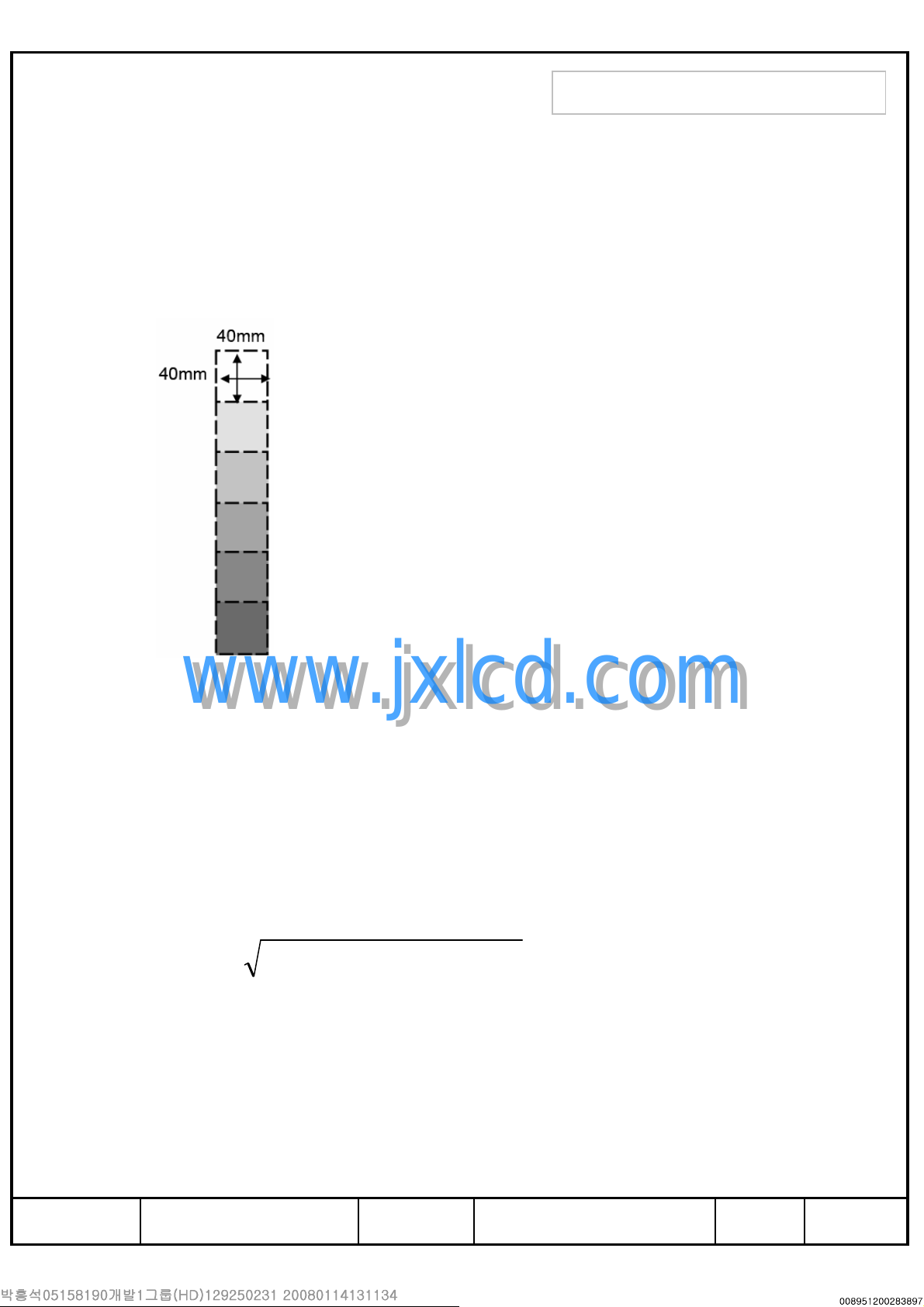
Note (9) Color Grayscale Linearity
a. Test image : 100% full white pattern with a test pattern as below
b. Test pattern : Squares, 40mm by 40mm in size, filled with 255, 225, 195, 165, 135 and
105 grays steps should be arranged at the center⑤ of the screen.
www.jxlcd.com
c. Test method
-1stgray step : move a square of 255 gray level should be moved into the center of the
screen and measure luminance and u’ and v’ coordinates.
- Next gray step : Move a 225 gray square into the center and measure both
luminance and coordinates, too.
d. Test evaluation
Where A, B : 2 gray levels found to have the largest color differences between them
i.e. get the largest Δu’ and Δv’ of each 6 pair of u’ and v’ and calculate the Δu’v’.
www.jxlcd.com
∆u'v'= (u' -u' ) +(v' -v' )
A B
2
A B
2
000_G_080114Doc No 10/34PageLTM190EP01MODEL
3. Electrical Characteristics
3.1 TFT LCD Module
The connector for display data & timing signal should be connected.
PRODUCT INFORMATION
PRODUCT INFORMATION
Ta = 25°C
NoteUnitMax.Typ.Min.SymbolItem
Voltage of Power Supply
Differential Input
Voltage for LVDS
Receiver Threshold
LVDS skew
LVDS
Input
Characteri
stics
Current of
Power
Supply
Differential input
voltage
Input voltage range
(single-ended)
Common mode
voltage
(a) Black
www.jxlcd.com
www.jxlcd.com
DD
SKEW
IN
V
CM
I
DD
0+
|VID|/2
1.2
2.4-
|VID|/2
(1)V5.55.04.5V
(2)mV+100--High
mV---100Low
(3)300-300t
(4)mV600200|VID|
(4)V2.40V
(4)V
mA1000900mA12001100-(b) White
mA14001200-(c) 1-dot
(5),(6)
Vsync Frequency
Hsync Frequency
Main Frequency
Rush Current
V
H
DCLK
RUSH
Note (1) The ripple voltage should be controlled under 10% of VDD.
Hz766049f
kHz856451f
MHz68.45440.9f
(7)A3.5--I
000_G_080114Doc No 11/34PageLTM190EP01MODEL
 Loading...