

Page 1
MODEL
LTA230AN03-W
Doc. No
Page
1 / 38
SAMSUNG Confidential
The Information described in this specification is for the first draft and can be changed without prior notice.
Samsung Display Co., LTD
SAMSUNG TFT-LCD
MODEL: LTA230AN03-W
Page 2
MODEL
LTA230AN03-W
Doc. No
Page
2 / 38
SAMSUNG Confidential
Contents
Revision History
General Description
1. Absolute Maximum Ratings
1.1 Environmental Absolute Ratings
1.2 Electrical Absolute Ratings
1.3 The Others Absolute Ratings
2. Optical Characteristics
3. Electrical Characteristics
3.1 TFT LCD Module
3.2 Backlight Unit
3.3 LED Module Connector
4. Block Diagram
4.1 TFT LCD Module
4.2 Back Light
5. Input Terminal Pin Assignment
5.1 Input Signal & Power
5.2 Converter Input Pin Configuration
5.3 Converter Input Power Sequence
5.4 LVDS Interface
5.5 Input Signals, Basic Display Colors and Gray Scale of Each Color
5.6 Pixel Format in the display
6. Interface Timing
6.1 The parameters of timing
6.2 Timing diagrams of interface signal
6.3 Characteristics of Input data of LVDS
6.4 The sequence of power on and off
7. Outline Dimension
8. Reliability Test
9.Marking & Others
10.General Precaution
10.1 Handling
10.2 Storage
10.3 Operation
10.4 Guide for the Operation Condition
10.5 Others
11. Special Precautions
- - - - - - - - - - - - - - - - - - - ( 3 )
- - - - - - - - - - - - - - - - - - - ( 4 )
- - - - - - - - - - - - - - - - - - - ( 6 )
- - - - - - - - - - - - - - - - - - - ( 7 )
- - - - - - - - - - - - - - - - - - - ( 13 )
- - - - - - - - - - - - - - - - - - - ( 16 )
- - - - - - - - - - - - - - - - - - - ( 17 )
- - - - - - - - - - - - - - - - - - - ( 23 )
- - - - - - - - - - - - - - - - - - - ( 32 )
- - - - - - - - - - - - - - - - - - - ( 33 )
- - - - - - - - - - - - - - - - - - - ( 35 )
- - - - - - - - - - - - - - - - - - - ( 36 )
- - - - - - - - - - - - - - - - - - - ( 39 )
Page 3
MODEL
LTA230AN03-W
Doc. No
Page
3 / 38
SAMSUNG Confidential
Date
Rev. No
Page
Summary
22. Fab. 2012
000
all
First Issued (First Draft)
The revision history
Page 4
MODEL
LTA230AN03-W
Doc. No
Page
4 / 38
SAMSUNG Confidential
General Description
Description
LTA230AN03 is a color active matrix liquid crystal display (LCD) that uses amorphous silicon TFT(Thin Film
Transistor) as switching components. This model is composed of a TFT LCD panel, a driver circuit, and a
back-light unit. This 23.0” model has a resolution of 1366 x 768 pixels (16:9) can display up to
16.7 Million colors with the wide viewing angle of 89° or higher in all directions. This panel is intended to
support applications by providing an excellent performance for the display products with a flat panel such as
Home-alone Multimedia TFT-LCD TV and a High Definition TV.
General Information
Features
High contrast ratio & aperture ratio with the wide color gamut
PVA(Patterned Vertical Align) mode
Wide viewing angle (±178°)
High speed response (with DCC circuit)
Wide XGA (1,366 x 768 pixels, 16:9)
Edge LED BLU Unit
DE (Data enable) mode
The interface (1 pixel/clock) of LVDS serial interface
Items
Specification
Unit
Note
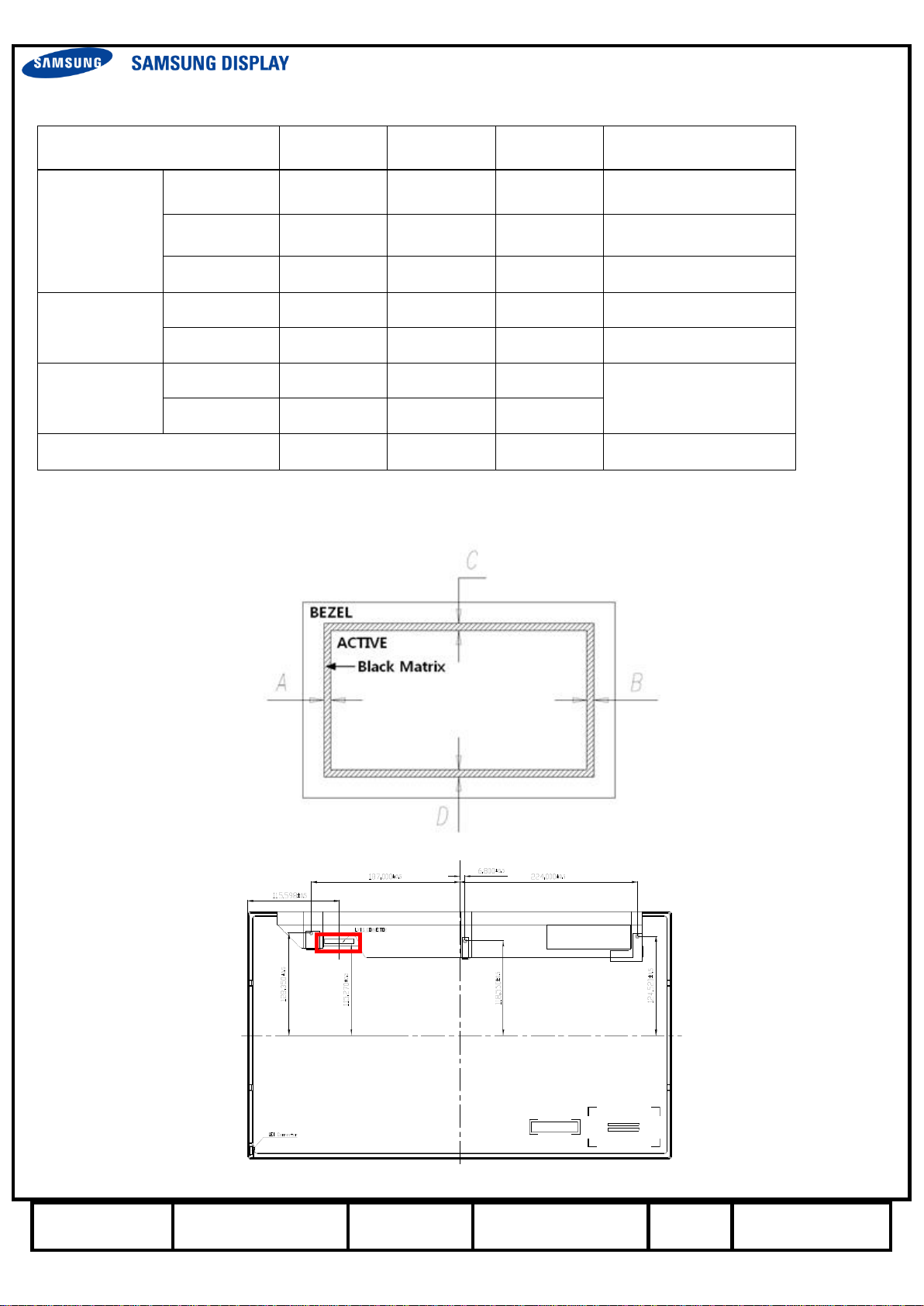
Module Size
534.0(H) x 311.8(V)
㎜
Max
11(D)
Max
Weight
1700
g
Typ
Pixel Pitch
0.372(H) x 0.124(W)
㎜
Active Display Area
508.152(H) x 285.696(V)
㎜
Surface Treatment
Anti-glare
Haze
2.3
%
Hardness
Hard coating 2H
Display Colors
16.7 Million colors (8 bits)
colors
Number of Pixels
1366 x 768
pixel
16 : 9
Pixel Arrangement
RGB horizontal stripe
Display Mode
Normally Black
Luminance of White
250
cd/m
2
Page 5
MODEL
LTA230AN03-W
Doc. No
Page
5 / 38
SAMSUNG Confidential
Item
Min.
Typ.
Max.
Note
Module size
Horizontal(H)
533.5
534.0
534.5
mm
Vertical(V)
311.3
311.8
312.3
mm
Depth(D)
10.5
11
11.5
mm(connector 위치)
Bezel Open
Horizontal(H)
513.3
513.8
514.3
mm
Vertical(V)
290.3
290.8
291.3
mm
Black Matrix
Shift
Horizontal(H)
2
mm
(1)
Vertical(V)
2
Weight
1700
g
NOTE (1) Measure the figure for Black Matrix shift to be recorded on the spec. with referring to the drawings.
| A - B | ≤ Horizontal Spec
| C - D | ≤ Vertical Spec
<Module Depth Measure Point : Chassis bottom Base Surface>
MECHANICAL INFORMATION
Page 6
MODEL
LTA230AN03-W
Doc. No
Page
6 / 38
SAMSUNG Confidential
1. ABSOLUTE MAXIMUM RATINGS
1.1 Environmental Absolute Ratings
Item
Symbol
Min.
Max.
Unit
Note
Storage temperature
TSTG
-20
65
C
(1)
Operating temperature
TOPR 0 50
C
(1)
Humidity for storagure
HSTG 5 90
%RH
Operating humidity
HOPR
20
90
%RG
Endurance on static electricity
150
V
(5)
Shock (non-operating)
Snop(X,Y)
50
G
(2),(4)
Snop(Z)
-
50
Vibration (non-operating)
Vnop - 1.5
G
(3),(4)
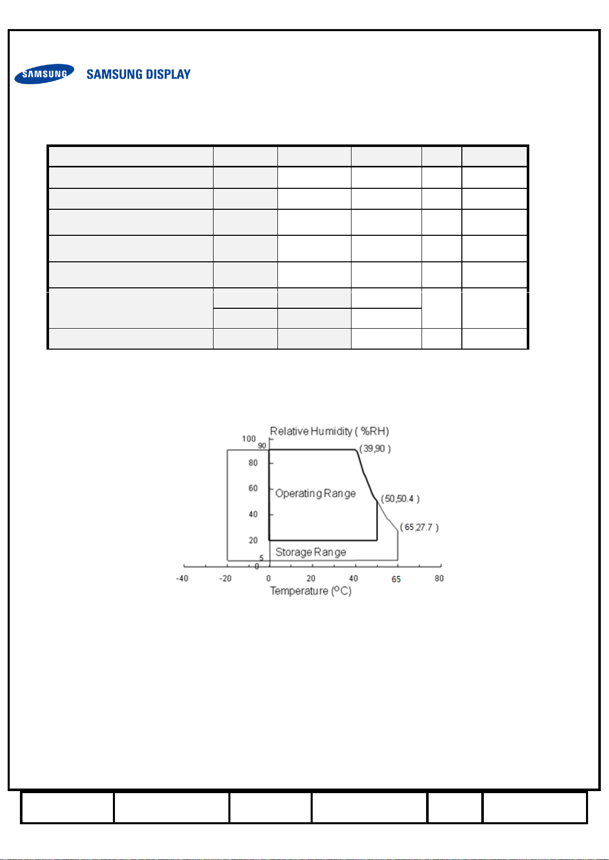
Note (1) The ranges of temperature and relative humidity are shown in the graph below. 90% RH Max.
(The temperature of Ta shall be over 39℃.)
The maximum temperature of wet–bulb shall be less than 39℃.
No condensation
Note (2) 11ms, half sine wave, one time for X, Y, Z axis
Note (3) 10 ~ 300 Hz, Swap rate for X, Y, Z axis one time*
Note (4) The fixture for the test of the vibration and shock, which holds the module to be tested shall be hard and
rigid in order for the module not to be twisted or bent by the fixture.
Note (5) Keep the static electricity under 50V in Polarizer attaching process.(Open Cell)
Page 7
MODEL
LTA230AN03-W
Doc. No
Page
7 / 38
SAMSUNG Confidential
Item
Symbol
Min.
Typ.
Max.
Unit
Note
Input Supply
Voltage /
Converter
Vcc
-
- - V
Without Converter
LED Current(2D)
ILED,2D
- - 180
mAmean
120mA/sting
, 1string
1.2 Electrical Absolute Ratings
(1) TFT LCD MODULE
1.3 The Others Absolute Ratings
STATIC ELECTRICITY PRESSURE RESISTANCE
Item
Symbol
Min.
Typ.
Max.
Unit
Note
Power Supply Voltage
VDD
10.8
12
13.2
V
(1)
Item
Test Conditions
Remark
CONTACT DISCHARGE
150pF, 330, 10kV, 210points, 1 time/point
Operating
AIR DISCHARGE
150pF, 330, 20kV, 210points, 1 time/point
Operating
(2) BACK-LIGHT UNIT
Note (1) Within Ta (25 2 C)
The permanent damage or defect to the device may occur if the panel is operated at the figure set, which exceeds a limit
of maximum value stated in the former spec.
The functional operation should be limited to the conditions described above under normal operating conditions.
Ta (25 2 C)
Page 8
MODEL
LTA230AN03-W
Doc. No
Page
8 / 38
SAMSUNG Confidential
2. Optical characteristics
The optical characteristics should be measured in the dark room or the space surrounded by the similar setting.
Measuring equipment : TOPCON RD-80S, TOPCON SR-3 ,ELDIM EZ-Contrast
(Ta = 25 ± 2°C, VDD=12.0V, fv=60Hz, f
DCLK
=148.5MHz, Light source: D65 Standard light)
Item
Symbol
Condition
Min.
Typ.
Max.
Unit
Note
Contrast ratio
(At the center of screen)
C/R
3000
4000
-
(1)
SR-3
Response
time
G-to-G
Tg
T
PAN,SUR
=29.9℃
- 8 16
msec
(3)
RD-80S
Luminance of white
(At the center of screen)
YL
Normal
qL,R=0
qU,D=0
Viewing
Angle
200
250
-
cd/m2
(4)
SR-3
Chromaticity
(CIE 1931)
Red
Rx
TYP.
-0.03
0.645
TYP.
+0.03
(5),(6)
SR-3
Ry
0.338
Green
Gx
0.302
Gy
0.603
Blue
Bx
0.149
By
0.067
White
Wx
0.285
Wy
0.311
sRGB Concordance
-
97
%
(5)
SR-3
Color gamut
- - 68 - %
Color
- -
8,500 - K
Viewing
Angle
Hor.
qL
C/R≥10
70
89
-
Degree
(6)
SR-3
EZ-Contrast
qR
70
89
-
Ver.
qU
70
89
-
qD
70
89
-
Brightness uniformity
(9 Points)
B
uni
-
-
25
%
(2)
SR-3
Transmissivity
T 5.3
5.7 - %
(7)
D65/SR3
Transmissivity Uniformity
T
uni
- - 10
%
(8)
D65/SR3
Gamma Value
GMA
(@20G~200G)
1.95
2.2
2.45
(9)
SR-3
Gamma variation
Gdiff
(@20G~128G)
-0.14 - 0.14
(11)
SR-3
ACC Linearity
ACC_lin
-0.015
-
0.015
(12)
SR-3
5nit Uniformity
(38G/255G)
Buni_5nit
-30 - 30
%
(10)
SR-3
White Color Coordinate
Uniformity
Wx uni
-
-
0.012
(13)
SR-3
Wy uni
0.012
Notice
Page 9
MODEL
LTA230AN03-W
Doc. No
Page
9 / 38
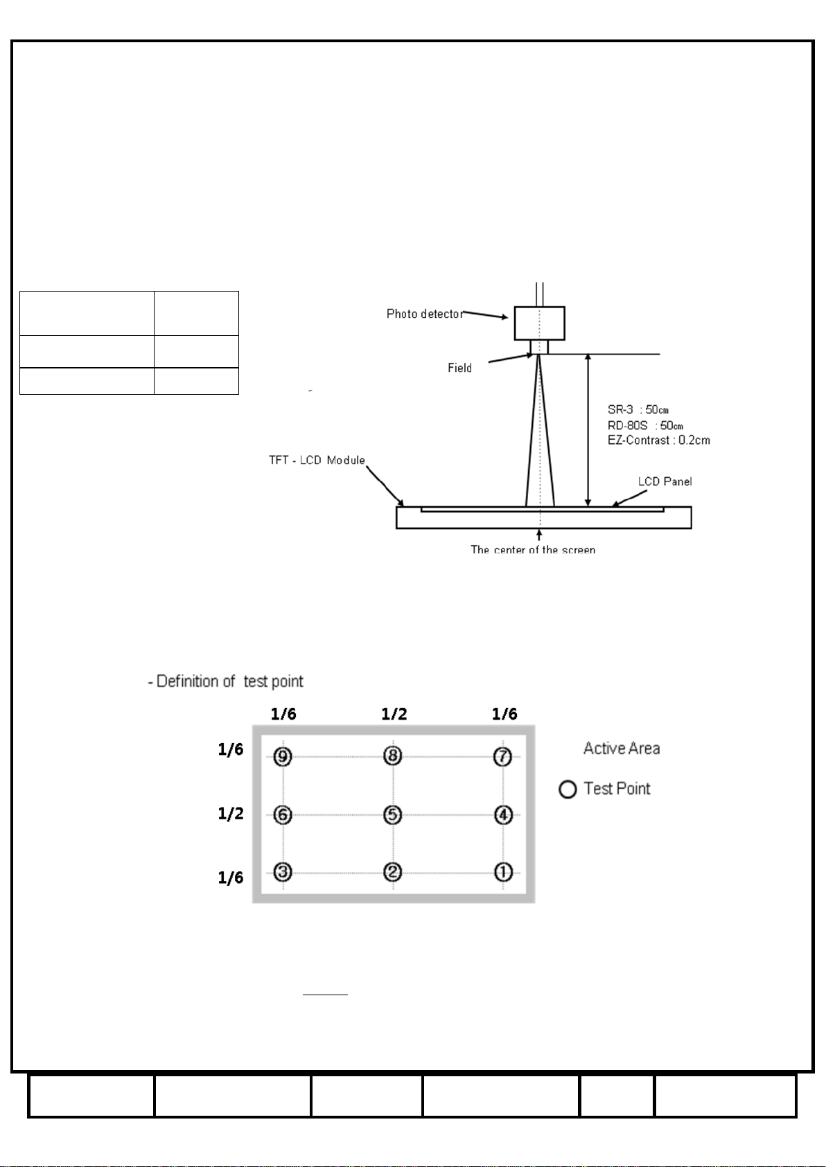
(a) Setup for test equipment
The measurement should be executed in a stable, windless, and dark room for 40min and 60min after
operating the panel at the given temperature for stabilization of the standard light. (SDC uses the standard
luminance of the D65 media).
This measurement should be measured at the center of screen.
The environment condition: Ta = 25 ± 2 °C
(b) D65 media has the general light source.
The temperature of color is 6847K. The coordinate of color is Wx 0.313, Wy 0.329
The luminance of this product is 7217cd/㎡.
Photo detector
Field
SR-3
2°/1°
RD-80S
1°
(c) The CIE positions D65 as the standard daylight illuminant:
[D65] is intended to represent average daylight and has a correlated color temperature of approximately
6500 K. CIE standard illuminant D65 should be used in all colorimetric calculations requiring
representative daylight, unless there are specific reasons for using a different illuminant.
Note (1) Definition of contrast ratio (C/R)
: The ratio of gray max (Gmax) & gray min (Gmin) at the center point ⑤ of the panel
The measurement goes in D65 Standard light source
Gmax : The luminance with all white pixels
C R
G
G
/
max
min
Page 10
MODEL
LTA230AN03-W
Doc. No
Page
10 / 38
Gmin : The luminance with all black pixels
Note (2) Definition of the brightness uniformity of 9 points (Test pattern : The full white)
The measurement shall be executed with the standard light source of D65 .
Bmax : The maximum brightness
Bmin : The minimum brightness
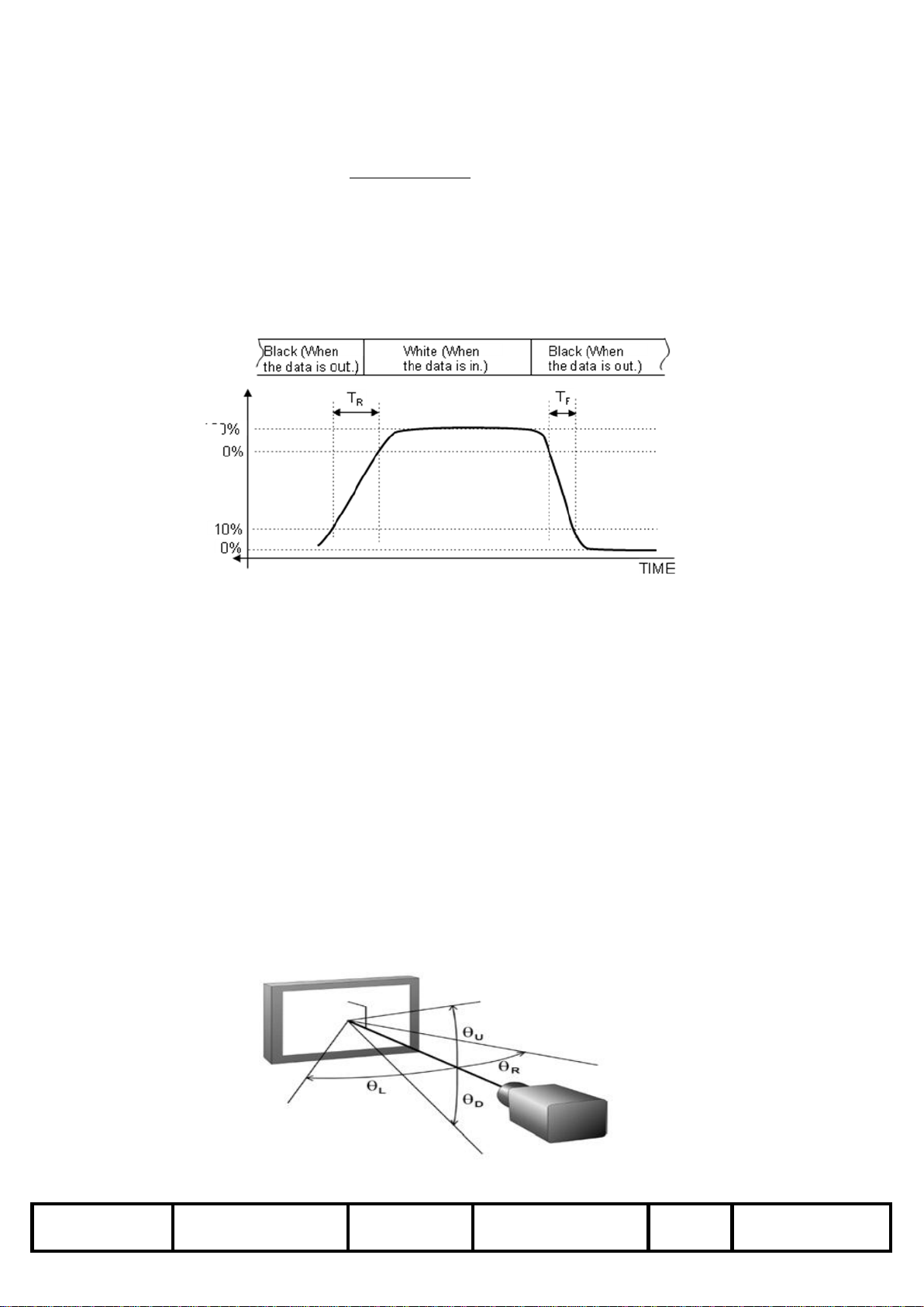
Note (3) Definition of the response time : Sum of Tr, Tf
※ G-to-G : Average response time between whole gray scale to whole gray scale.
The response time is the value that was measured after it was operated in Samsung's standard BLU for
one hour.( at room temperature)
Note (4) The definition of luminance of white: The luminance of white at the center point ⑤
The measurement shall be executed with the standard light source of D65.
Note (5) The definition of chromaticity (CIE 1931)
The color coordinate of red, green, blue and white at the center point ⑤
The measurement shall be executed with the standard light source of D65.
Note (6) Definition of viewing angle
: The range of viewing angle (C/R ≥10)
The measurement shall be executed with the standard light source of D65.
The response
Of optical instruments
Buni
B B
B
100
( max min)
max
Display data
Page 11
MODEL
LTA230AN03-W
Doc. No
Page
11 / 38
SAMSUNG Confidential
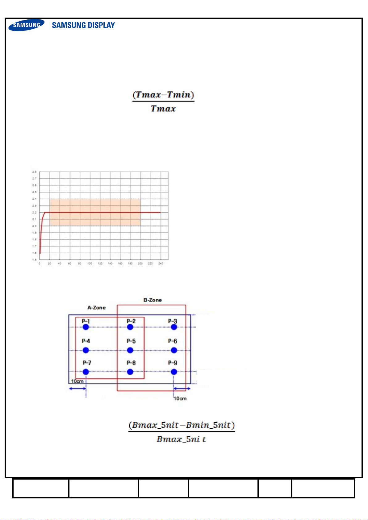
Note (7) Definition of transmissivity
The measurement shall be executed with the standard light source of D65.
Note (8) Definition of the Transmissivity uniformity of 9 points (Test pattern: The full white)
The measurement shall be executed with the standard light source of D65.
Tmax : The maximum Transmissivity
Tmin : The minimum Transmissivity
Note (9) Management Criteria of Gamma Value
Note (10) 5nit Low Gray Uniformity
Tuni
= 100*
Gamma Value :
20 ~ 200Gray : 2.0 ~ 2.4 (Typ. 2.2)
Buni_5nit
= 100*
Bmax_5nit : The maximum brightness at 5nit Gray
Bmin_5nit : The minimum brightness at 5nit Gray
Vertical 1/6 Point
[Panel Measure Point]
Vertical 1/6 Point
Page 12
MODEL
LTA230AN03-W
Doc. No
Page
12 / 38
Note (11) Gamma Variation between Center and Left (or Right)
Gamma measured at 10cm point from the left & right side is more less than 0.1 than Gamma measured
at Center
(Gamma measured at 10cm of the P-4 & P-6 is more less than 0.1 than Gamma measured at P-5)
Note (12) Management Criteria of ACC Linearity
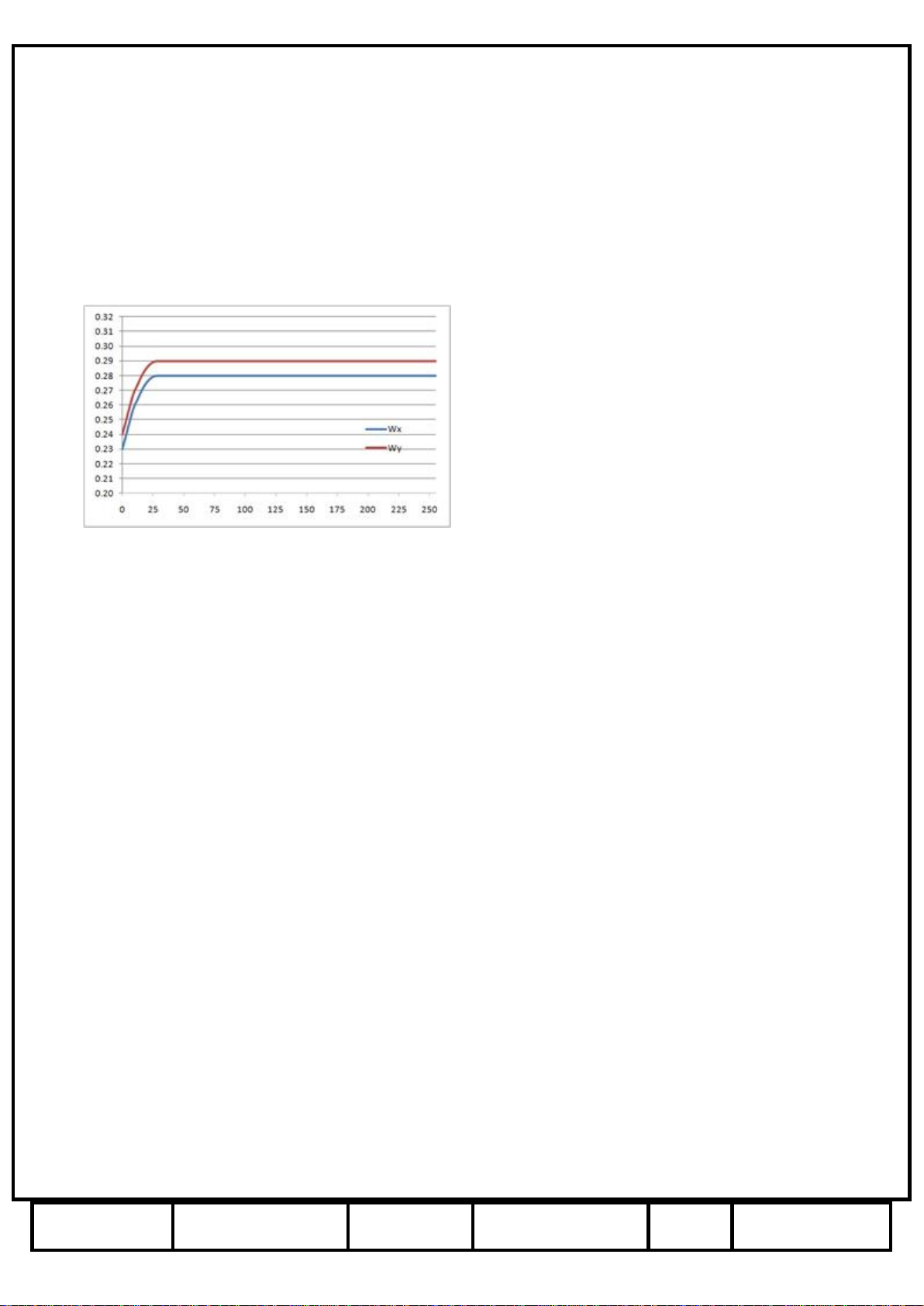
Note (13) White Color Coordinate Uniformity of 9 points (Test pattern: The full white)
< Frame Inversion >
255Gray Wx/Wy value basis (a module unit basis)
a. Color coordinate differences are less than 15/1,000 at
Any Point above 30Gray and 255Gray
b. When Wx/Wy coordinates reverse at 0Gray, it permits
an once intersection under, 30Gray
Wy, uni
= Wy max-Wy min
Wy max: The maximum Wy
Wy min: The minimum Wy
Page 13

MODEL
LTA230AN03-W
Doc. No
Page
13 / 38
SAMSUNG Confidential
3. Electrical characteristics
The connector to transmit a display data and a timing signal shall be connected.
Ta = 25°C ± 2 °C
Item
Symbol
Min.
Typ.
Max.
Unit
Note
Voltage of power supply
V
DD
10.8
12.0
13.2
V
(1)
Current
of power
supply
(a) Black
I
DD
-
201
301
mA
(2),(3)
(b) White
-
216
316
mA
(c) V-stripe
-
368
524
mA
Vsync frequency
f
V
48
60
66
Hz Hsync frequency
f
H
44
48
53
kHz Main frequency
f
dclk
72
78
85
MHz Rush current
I
RUSH
- - 4
A
(4)
Note (1) The voltage for ripple shall be controlled under the range of fewer than 10% of V
DD
voltage.
(2) fV=60Hz, f
DCLK
=78MHz, VDD = 12.0V, DC Current.
(3) The pattern for checking the power dissipation (LCD module only)
(4) Conditions for measurement
3.1 TFT_LCD Module
a) Black pattern b) White pattern c) V-stripe
Page 14

MODEL
LTA230AN03-W
Doc. No
Page
14 / 38
* The temperature range for component of the some major part of operating module
3.2 BACK-LIGHT UNIT
* Back light unit is composed of 1–LED bars .(33 pcs of LEDs).
Item
Symbol
Min.
Typ.
Max.
Unit
Note
LED Operating
Temperature range
Top
-30 - 85
℃
LED unit
LED Storage
Temperature range
Tstg
-40
-
100
℃
LED Junction
Temperature
Tj - -
145
℃
LED Forward Current
IF - 120
126
mA
1 channel
IFP
-
N/A - mA
N/A
LED Forward Voltage
VF
96.4
103.6
110.9
V
VFP
-
N/A - V
N/A
Thermal Resistance
Junction to PCB
Rth, JS
- - 18
K/W
Power Consumption
P
11.6
12.4
13.3
W
IF X VF X 1CH
Operating Life Time
Hr
>30,000
Hour
LED Counts
Q - 33 - EA
Part
Spec
Ambient Operating
Temperature
Junction Operating
Temperature
Timing Controller
LAXC021T2B-Q1
-20℃ ~ 75℃
~ 125℃
Ta=25℃
Page 15

MODEL
LTA230AN03-W
Doc. No
Page
15 / 38
* Pin Description (Connector : 104086-0410, Molex)
pin
name
description
1
Vin
LED power input
2
-
-
3
-
-
4
RTN
LED Bar return channel
3.3 LED Module Connector
Page 16

MODEL
LTA230AN03-W
Doc. No
Page
16 / 38
4. Block diagram
without converter, 33 LEDs
** Vin 120mA current supply
** I1 = 120mA(typ)
4.1 TFT LCD MODULE
4.2 Back Light
Page 17

MODEL
LTA230AN03-W
Doc. No
Page
17 / 38
SAMSUNG Confidential
5. The Pin assignment in the input terminal
connector : PTW (30Pin,SMD-A)
No
Signal
REMARK
1
WPN
WPN
2
SCL
I2C interface
3
SDA
4
GND
GND
5
LV0_N
negative LVDS differential data input (0)
6
LV0_P
positive LVDS differential data input (0)
7
GND
GND
8
LV1_N
negative LVDS differential data input (1)
9
LV1_P
positive LVDS differential data input (1)
10
GND
GND
11
LV2_N
negative LVDS differential data input (2)
12
LV2_P
positive LVDS differential data input (2)
13
GND
GND
14
LVCLK_N
negative LVDS differential data input (Clock)
15
LVCLK_P
positive LVDS differential data input (Clock)
16
GND
GND
17
LV3_N
negative LVDS differential data input (3)
18
LV3_P
positive LVDS differential data input (3)
19
GND
GND
20
N.C
21
LVDS_SEL
LVDS OPTION (Low: JEIDA, High: VESA)
22
WPN
WPN
23
GND
GND
24
GND
25
N.C
26
VIN
Power Supply : +12V
27
VIN
28
VIN
29
VIN
30
VIN
5.1 Input Signal & Power
Page 18

MODEL
LTA230AN03-W
Doc. No
Page
18 / 38
SAMSUNG Confidential
Note(1) : Pin number, which starts from the left side.
a. Pins for power GND shall be connected to the LCD’s metal chassis.
b. All input pins for power shall be connected together.
c. All NC pins shall be designed with being separated from other signal or power.
Fig . The diagram of connector
Page 19

MODEL
LTA230AN03-W
Doc. No
Page
19 / 38
Without converter product
Without converter product
5.2 Configuration of Input pin of Converter
5.3 The power sequence for inputting the Converter
Page 20

MODEL
LTA230AN03-W
Doc. No
Page
20 / 38
SAMSUNG Confidential
5.4 LVDS Interface
- LVDS Receiver : T-CON (merged)
- Data Format(Normal)
LVDS pin
JEIDA -DATA
Normal -DATA
TxOUT/RxIN0
TxIN/RxOUT0
R2
R0
TxIN/RxOUT1
R3
R1
TxIN/RxOUT2
R4
R2
TxIN/RxOUT3
R5
R3
TxIN/RxOUT4
R6
R4
TxIN/RxOUT6
R7
R5
TxIN/RxOUT7
G2
G0
TxOUT/RxIN1
TxIN/RxOUT8
G3
G1
TxIN/RxOUT9
G4
G2
TxIN/RxOUT12
G5
G3
TxIN/RxOUT13
G6
G4
TxIN/RxOUT14
G7
G5
TxIN/RxOUT15
B2
B0
TxIN/RxOUT18
B3
B1
TxOUT/RxIN2
TxIN/RxOUT19
B4
B2
TxIN/RxOUT20
B5
B3
TxIN/RxOUT21
B6
B4
TxIN/RxOUT22
B7
B5
TxIN/RxOUT24
HSYNC
HSYNC
TxIN/RxOUT25
VSYNC
VSYNC
TxIN/RxOUT26
DEN
DEN
TxOUT/RxIN3
TxIN/RxOUT27
R0
R6
TxIN/RxOUT5
R1
R7
TxIN/RxOUT10
G0
G6
TxIN/RxOUT11
G1
G7
TxIN/RxOUT16
B0
B6
TxIN/RxOUT17
B1
B7
TxIN/RxOUT23
RESERVED
RESERVED
LVDS OPTION( input : pin45 ) : IF THIS PIN : LOW (GND) → JEIDA LVDS FORMAT
OTHERWISE : HIGH (3.3V) OR OPEN(NC) → NORMAL NS LVDS FORMAT
Page 21

MODEL
LTA230AN03-W
Doc. No
Page
21 / 38
SAMSUNG Confidential
COLOR
DISPLAY
DATA SIGNAL
GRAY
SCALE
LEVEL
RED
GREEN
BLUE
R0
R1
R2
R3
R4
R5
R6
R7
G0
G1
G2
G3
G4
G5
G6
G7
B0
B1
B2
B3
B4
B5
B6
B7
BASIC
COLOR
BLACK
0 0 0 0 0 0 0 0 0 0 0 0 0 0 0 0 0 0 0 0 0 0 0 0 -
BLUE
0 0 0 0 0 0 0 0 0 0 0 0 0 0 0 0 1 1 1 1 1 1 1 1 -
GREEN
0 0 0 0 0 0 0 0 1 1 1 1 1 1 1 1 0 0 0 0 0 0 0 0 -
CYAN
0 0 0 0 0 0 0 0 1 1 1 1 1 1 1 1 1 1 1 1 1 1 1 1 -
RED
1 1 1 1 1 1 1 1 0 0 0 0 0 0 0 0 0 0 0 0 0 0 0 0 -
MAGENTA
1 1 1 1 1 1 1 1 0 0 0 0 0 0 0 0 1 1 1 1 1 1 1 1 -
YELLOW
1 1 1 1 1 1 1 1 1 1 1 1 1 1 1 1 0 0 0 0 0 0 0 0 -
WHITE
1 1 1 1 1 1 1 1 1 1 1 1 1 1 1 1 1 1 1 1 1 1 1 1 -
GRAY
SCALE
OF RED
BLACK
0 0 0 0 0 0 0 0 0 0 0 0 0 0 0 0 0 0 0 0 0 0 0 0 R0
DARK
↑
↓
LIGHT
1 0 0 0 0 0 0 0 0 0 0 0 0 0 0 0 0 0 0 0 0 0 0 0 R1
0 1 0 0 0 0 0 0 0 0 0 0 0 0 0 0 0 0 0 0 0 0 0 0 R2 : : : : : : : : : : : : : : : : : : : : : : : :
R3~
R252
: : : : : : : : : : : : : : : : : : : : : : :
:
1 0 1 1 1 1 1 1 0 0 0 0 0 0 0 0 0 0 0 0 0 0 0 0 R253
0 1 1 1 1 1 1 1 0 0 0 0 0 0 0 0 0 0 0 0 0 0 0 0 R254
RED
1 1 1 1 1 1 1 1 0 0 0 0 0 0 0 0 0 0 0 0 0 0 0 0 R255
GRAY
SCALE
OF
GREEN
BLACK
0 0 0 0 0 0 0 0 0 0 0 0 0 0 0 0 0 0 0 0 0 0 0 0 G0
DARK
↑
↓
LIGHT
0 0 0 0 0 0 0 0 1 0 0 0 0 0 0 0 0 0 0 0 0 0 0 0 G1
0 0 0 0 0 0 0 0 0 1 0 0 0 0 0 0 0 0 0 0 0 0 0 0 G2
: : : : : : : : : : : : : : : : : : : : : : :
:
G3~
G252
: : : : : : : : : : : : : : : : : : : : : : : : 0 0 0 0 0 0 0 0 1 0 1 1 1 1 1 1 0 0 0 0 0 0 0 0 G253
0 0 0 0 0 0 0 0 0 1 1 1 1 1 1 1 0 0 0 0 0 0 0 0 G254
GREEN
0 0 0 0 0 0 0 0 1 1 1 1 1 1 1 1 0 0 0 0 0 0 0 0 G255
GRAY
SCALE
OF
BLUE
BLACK
0 0 0 0 0 0 0 0 0 0 0 0 0 0 0 0 0 0 0 0 0 0 0 0 B0
DARK
↑
↓
LIGHT
0 0 0 0 0 0 0 0 0 0 0 0 0 0 0 0 1 0 0 0 0 0 0 0 B1
0 0 0 0 0 0 0 0 0 0 0 0 0 0 0 0 0 1 0 0 0 0 0 0 B2
: : : : : : : : : : : : : : : : : : : : : : :
:
B3~
B252
: : : : : : : : : : : : : : : : : : : : : : :
:
0 0 0 0 0 0 0 0 0 0 0 0 0 0 0 0 1 0 1 1 1 1 1 1 B253
0 0 0 0 0 0 0 0 0 0 0 0 0 0 0 0 0 1 1 1 1 1 1 1 B254
BLUE
0 0 0 0 0 0 0 0 0 0 0 0 0 0 0 0 1 1 1 1 1 1 1 1 B255
Note ) Definition of Gra
Rn : Red Gray, Gn : Green Gray, Bn : Blue Gray (n = Gray level)
Input Signal : 0 = Low level voltage, 1 = High voltage
5.5 Input Signals, Basic display colors and Gray Scale of Each Color
Page 22

MODEL
LTA230AN03-W
Doc. No
Page
22 / 38
SAMSUNG Confidential
5.6 Pixel Format in the display
Line 1
Line 768
1
1366
Page 23

MODEL
LTA230AN03-W
Doc. No
Page
23 / 38
6. Interface timing
6.1 The parameters of timing ( DE mode )
SIGNAL
ITEM
SMBOL
MIN.
TYP.
MAX.
Unit
NOTE
Clock
Frequency
1/T
C
72
78
85
MHz
-
Hsync
F
H
44
48
53
KHz
-
Vsync
F
V
48
60
66
Hz
-
Term for the
vertical
display
Active
display
period
T
VD
-
768
-
Lines
-
Total vertical
T
V
780
802
1200
Lines
-
Term for the
horizontal
display
Active
display
period
T
HD
-
1366
-
Clocks
-
Total
Horizontal
T
H
1460
1624
2000
clocks
-
Note) The signals of Hsync and Vsync must be inputted even though this T-con is operated at DE mode.
(1) Test Point: TTL controls signal and CLK at LVDS Tx at the input terminal of system.
(2) Internal VDD = 3.3V
(3) The spread spectrum
- The limit of spread spectrum's range of SET in which the LCD module is assembled should be within ± 3 %
- Frequency for modulation : Min 30KHz
Parameter
Symbol
Value
Unit
Note
Min
Typ
Max
CMOS
Interface
Input High
Threshold
Voltage
VIH (High)
2.5
-
3.3 V
Input Low
Threshold
Voltage
VIL (Low)
0 - 0.5 V
Page 24

MODEL
LTA230AN03-W
Doc. No
Page
24 / 38
SAMSUNG Confidential
6.2 Timing diagrams of interface signal (Only DE mode)
Page 25

MODEL
LTA230AN03-W
Doc. No
Page
25 / 38
R03
RxOUT26 RxOUT25 RxOUT22
RxOUT24
RxOUT21 RxOUT20 RxOUT19
RxOUT18 RxOUT15 RxOUT13RxOUT14 RxOUT12 RxOUT9 RxOUT8
RxOUT7 RxOUT6 RxOUT3RxOUT4 RxOUT2 RxOUT1 RxOUT0
T
DE Vsync B02Hsync B05 B03 B04
G04 B01 G05 B00 G03 G02 G01
G00 R04 R05 R02 R01 R00
TxCLK OUT
RxCK IN
Rx IN1
Rx IN0
Rx IN2
RxOUT23 RxOUT17 RxOUT11
RxOUT16
RxOUT10 RxOUT5 RxOUT27
T/7
B07 R06B06 G07 R07 G06
Rx IN3
RESERVED
RECOMMENDED TRANSMITTER INPUT CHARACTERISTICS
SYMBOL
PARAMETER
MIN.
TPY.
MAX.
UNITS.
TCIT
TxCLK IN TRANSITION TIME (FIG2)
1.0
-
6.0
ns
TCIP
TxCLK IN PERIOD (FIG3)
11.76
T
50
ns
TCIH
TxCLK IN HIGH TIME (FIG3)
0.35T
0.5T
0.65T
ns
TCIL
TxCLK IN LOW TIME (FIG3)
0.35T
0.5T
0.65T
ns
TXIT
TxCLK TRANSITION TIME
1.5
-
6.0
ns
Page 26

MODEL
LTA230AN03-W
Doc. No
Page
26 / 38
TRANSMITTER SWITCHING CHARACTERISTICS
-OVER RECOMMENDED OPERATING SUPPLY AND TEMPERATURE RANGES UNLESS OTHERWISE SPECIFIED.
SYMBOL
PARAMETER
MIN.
TPY.
MAX.
UNITS.
LLHT
LVDS LOW TO HIGH TRANSITION TIME (FIG1)
-
0.75
1.5
ns
LHLT
LVDS HIGH TO LOW TRANSITION TIME (FIG1)
-
0.75
1.5
ns
TPPos0
TRANSMITTER OUTPUT PULSE POSITION FOR BIT 0 (FIG 7)
NOTE 1
F = 40MHZ
-0.25 0 0.25
ns
TPPos1
TRANSMITTER OUTPUT PULSE POSITION FOR BIT 1
3.32
3.57
3.82
ns
TPPos2
TRANSMITTER OUTPUT PULSE POSITION FOR BIT 2
6.89
7.14
7.39
ns
TPPos3
TRANSMITTER OUTPUT PULSE POSITION FOR BIT 3
10.46
10.71
10.96
ns
TPPos4
TRANSMITTER OUTPUT PULSE POSITION FOR BIT 4
14.04
14.29
14.54
ns
TPPos5
TRANSMITTER OUTPUT PULSE POSITION FOR BIT 5
17.61
17.86
18.11
ns
TPPos6
TRANSMITTER OUTPUT PULSE POSITION FOR BIT 6
21.18
21.43
21.68
ns
TPPos0
TRANSMITTER OUTPUT PULSE POSITION FOR BIT 0 (FIG 7)
NOTE 1
F = 65MHZ
-0.20 0 0.20
ns
TPPos1
TRANSMITTER OUTPUT PULSE POSITION FOR BIT 1
2.00
2.20
2.40
ns
TPPos2
TRANSMITTER OUTPUT PULSE POSITION FOR BIT 2
4.20
4.40
4.60
ns
TPPos3
TRANSMITTER OUTPUT PULSE POSITION FOR BIT 3
6.39
6.59
6.79
ns
TPPos4
TRANSMITTER OUTPUT PULSE POSITION FOR BIT 4
8.59
8.79
8.99
ns
TPPos5
TRANSMITTER OUTPUT PULSE POSITION FOR BIT 5
10.79
10.99
11.19
ns
TPPos6
TRANSMITTER OUTPUT PULSE POSITION FOR BIT 6
12.99
13.19
13.39
ns
TPPos0
TRANSMITTER OUTPUT PULSE POSITION FOR BIT 0 (FIG 7)
NOTE 1
F = 85MHZ
-0.20 0 0.20
ns
TPPos1
TRANSMITTER OUTPUT PULSE POSITION FOR BIT 1
1.48
1.68
1.88
ns
TPPos2
TRANSMITTER OUTPUT PULSE POSITION FOR BIT 2
3.16
3.36
3.56
ns
TPPos3
TRANSMITTER OUTPUT PULSE POSITION FOR BIT 3
4.84
5.04
5.24
ns
TPPos4
TRANSMITTER OUTPUT PULSE POSITION FOR BIT 4
6.52
6.72
6.92
ns
TPPos5
TRANSMITTER OUTPUT PULSE POSITION FOR BIT 5
8.20
8.40
8.60
ns
TPPos6
TRANSMITTER OUTPUT PULSE POSITION FOR BIT 6
9.88
10.08
10.28
ns
TSTC
TxIN SETUP TO TxCLK IN (FIG 3)
2.5 - -
ns
THTC
TxIN HOLD TO TxCLK IN (FIG 3)
0 - -
ns
TCCD
TxCLK IN TO TxCLK OUT DELAY (FIG4)
Ta = 25 ℃, Vcc = 3.3
V
3.8 - 6.3
ns
TxCLK IN TO TxCLK OUT DELAY (FIG4)
2.8 - 7.1
ns
TJCC
TRANSMITTER JITTER CYCLE TO CYCLE (FIG 8,9)
F=85 MHZ
-
110
150
ps
F=65 MHZ
-
210
230
ps
F=40 MHZ
-
350
370
ps
TPLLS
TRANSMITTER PHASE LOCK LOOP SET (FIG 5)
- - 10
ms
TPDD
TRANSMITTER POWER DOWN DELAY (FIG 6)
- - 100
ns
Page 27

MODEL
LTA230AN03-W
Doc. No
Page
27 / 38
note1)The minimum and maximum limits are based on statistical analysis of the device performance over process, voltage, and temperature
ranges. this parameter is functionality tested only on automatic test equipment (ATE)
note2)The limits are based onbench charaterization of the device's jitter response over the power supply voltage range. output clock jitter is
measured with a cycle to cycle jitter of ± 3ns applied to the input clock signal while data inputs are switching (fig8,9).A jitter event of 3 ns,
represents worse case jump in the clock edge from most graphics controller VGA Cihps currently available. this parameter is used when calculating
system margin as descrbed in AN-1059
Page 28

MODEL
LTA230AN03-W
Doc. No
Page
28 / 38
Page 29

MODEL
LTA230AN03-W
Doc. No
Page
29 / 38
Page 30

MODEL
LTA230AN03-W
Doc. No
Page
30 / 38
SAMSUNG Confidential
6.3 Characteristics of Input data of LVDS (S64V 기준)
(1) DC Specification
(2) AC Specification
Page 31

MODEL
LTA230AN03-W
Doc. No
Page
31 / 38
Page 32

MODEL
LTA230AN03-W
Doc. No
Page
32 / 38
SAMSUNG Confidential
6.4 The sequence of power on and off
To prevent a latch-up phenomena or the DC operation of the LCD Module, the power on/off sequence should be
accorded with the settings described in the diagram below.
T1 SPEC : 0.5 msec<T1≤10msec
T2 SPEC : 10 msec<T2≤50msec
T3 SELC : 0msec<T3≤50msec
T4 SELC : 1000msec≤T4
T5 SELC : 1000msec≤T5 (BLU ON TIME : Converter ENA Signal(ON))
T6 SELC : 100msec≤T6 (BLU OFF TIME : Converter ENA Signal(OFF))
T1 : The time, during which the level of VDD is rising from 10% to 90%.
T2 : The change for the time, during which the V
DD
start rising the level above 90% until the valid data of signal started coming in.
T3 : The change for the time, during which the valid data of signal started coming until the VDD started coming out.
T4 : The time, during which the V
DD
start coming out to restart the Windows.
T5 : The time, during which the valid data starts coming in until the power of B/L exceed 50%.
T6 : The time, during which the level of B/L’s power falls below 50% until the valid data of signal starts coming out.
The inputted V
DD
’s value for supply voltage, BLU, and signal to the external system of the module shall be
computed in observance of the former mentioned value.
The method to apply the voltage to the lamp within the range, which the LCD operates. When the back-
light is turned on before the LCD is operated or the power of LCD is turned off before the back-light is
turned off, the abnormal display on the screen may be shown momentarily.
Please keep the level of input signal low or keep the level of impedance high when the V
DD
is off.
The value shall be measured after the module has been fully discharged between the periods when the
power is on and off during the T4.
Page 33

MODEL
LTA230AN03-W
Doc. No
Page
33 / 38
SAMSUNG Confidential
7. Outline dimension
Page 34

MODEL
LTA230AN03-W
Doc. No
Page
34 / 38
SAMSUNG Confidential
8. Reliability test
Items to be evaluated
Condition for the evaluation
Quantity
Standard for evaluation
HTOL
50 ℃
4
60 ℃
8
LTOL
-5℃
4
THB
Evaluate the whole cell in the panel when examining the
panel, which is over 32" at 50℃ and 90 %RH.*
10
Margin on the operation
of ASG at a low
temperature.
(Optional)
Check the temperature when the noise occurs under the
conditions, the max. frequency and between the 40℃ and 25℃.
Each cell
Applied to products with
ASG only.
Margin on the operation
of ASG at a high
temperature. (Optional)
Examine the panel operated under the conditions, the
min. frequency and the 60℃ for 96hrs.
Each cell
Applied to products with
ASG only.
Residual image at a
normal temp.
Repeat the exam. to examine the mosaic pattern(9"*10")
of panel at 25 ℃ for 12hrs followed by the exam for the
rolling pattern at 25 ℃ for 12hrs three times.
8
New decompression
Examine the panel, which is in the temp. range of 40℃ to 50℃ between the
0m(0ft) and 13,700m(45,000ft) for
72 and half hrs.
4
HTS
Store at the 70 ℃.
4
LTS
Store at the -25 ℃.
4
Residual image at the
high temperature
(optional)
Examine the mosaic pattern(9"*10") of DID at
50℃ for 336hrs.
8
Only for DID product
Evaluation for the
panel on the pallet
Dropping(20cm)->Set the temp. and humidity(30℃~60℃ / 40℃~90%RH)->Pressurizing-
> Vibrating(Vibrate the panel within the frequency range
between 5hz and 200hz for 2hrs at the sine wave of 1.05
g.)->Dropping(20cm)
1 Pallet
Vibration
Vibrate the panel within the frequency range between
10hz and 300hz for 10min at the sine wave at 1.5G
Vibrate the panel in the direction of X, Y, and Z axis for
30min.
3
Shock
If the screen size of panel is below 40", drop the panel
with applying the 50G one time toward the direction of
±X, Y, and Z axis from the spot where the panel is
placed respectively for 11msec. (±XYZ), If the screen size
is 46“, apply the 40G for ±X and Y axis or the 30G for ±
Z. If the screen size is over 52", apply the 30G.
3
TSS
Test the TV between the -20℃ and 65℃ 440 times. Test
the DID between the -20℃ and 65℃ 220 times.
4
WHTS
Store the module at 60 ℃ and 75 %RH.
4
TS
Execute the exam for TV at -20℃ for 30 min. and at
60℃ for 30min 100 times. / Execute the exam for the
DID at -20℃ for 30 min. and at 60℃ for 30min 200
times.
4
Dust
Execute the test to observe the status of falling dust for
2
Page 35

MODEL
LTA230AN03-W
Doc. No
Page
35 / 38
5 min. after spraying the dust in the air for 5 sec. at a
normal temperature and normal humidity for 5 hrs.
Turn the panel on and off at the interval of 10 min.
Execute the test for the DID for 10hrs.
Twist
Examine the 52”-sized module by pushing the one point
of panel by 10 degrees forward and backward with
fixing other three points for 0.9s 500 times respectively.,
Examine the 46”-sized module by pushing the one point
of panel by 10 degrees forward and backward with
fixing other three points for 0.7s 500 times respectively.
Examine the 40"-sized module by pushing the one point
of panel by 20 degrees forward and backward with
fixing other three points for 0.85s 250 times
respectively., Examine the 32”-sized module by pushing
the one point of panel by 20 degrees forward and
backward with fixing other three points for 0.7s 250
times respectively.
Examine the 26”-sized module by pushing the one point
of panel by 20 degrees forward and backward with
fixing other three points for 0.6s 250 times respectively.
4
Noise
Noise occurred when the frame of instrument is
expanded as the operating module emits the heat.: Max
50dB (Below the 10 times when the level of sound is
over 36dB.)
2
Noise
Noise from machine : Under the 23dB on average.
2
The new compound
stress
Repeat the exam, which stresses the panel under the
temp. range of -20℃ to 60℃ and the humidity range
of 0%RH to 90%RH two times.
4
ESD
Shoot the ESD with the measuring gun,
which is operated at ±10 kV to the 210 points with
contacting the panel.
3
Shoot the ESD with the measuring gun, which is
operated at ±20 kV to the 210 points without
contacting the panel.
3
Input pin for inverter and converter (optional): Apply ±
15kV three times.
3
Only for the attached part
of inverter and converter.
[ Criteria on evaluation]
The components of product, which may affect to the function of display shall not be changed when the display
quality test is executed under the normal operating condition.
* HTOL/ LTOL : The operating at the high and low temperature*
* THB : The slant of temperature and humidity
* HTS/LTS : The storage at the high and low temperature
* WHTS : The storage condition at the high temperature with the high humidity
Page 36

MODEL
LTA230AN03-W
Doc. No
Page
36 / 38
SAMSUNG Confidential
10.2 Storage
ITEM
Unit
Min.
Max.
Storage
Temperature
(℃)
5
40
Storage
Humidity
(%rH)
35
75
Storage life
12 months
Storage
Condition
- The storage room shall be equipped with a good ventilation facility, which has
a temperature controlling system.
- Products shall be placed on the pallet, which is away from the wall not on the floor.
- Prevent products from being exposed to the direct sunlight, moisture, and water.;
Be cautious not to pile the products up.
- Avoid storing products in the environment where other hazardous material is placed.
- If products are delivered or kept in the storage facility more than 3 months, we recommend
you to leave products under the condition including a 20℃ temperature and a humidity of
50% for 24 hours.
10.3 Operation
(1) Do not connect or disconnect the cable to the module at the "Power On" condition.
(2) The power shall be always turned on/off by the item 6.4. "Power on/off sequence"
(3) The module has a circuit with a high frequency. The electromagnetic interference shall be suppressed by
system manufacturers sufficiently. The methods to ground and shield is important to minimize the
interference.
(4) Design the length of cable to connect between the connector for back-light and the inverter as short as possible
and the shorter cable shall be connected directly.
The cable between the back light connector and its converter power supply should be connected directly with
a minimized length. A longer cable between the back light and the converter may cause lower luminance of
LED package and may require higher startup voltage(Vs).
Page 37

MODEL
LTA230AN03-W
Doc. No
Page
37 / 38
SAMSUNG Confidential
10.4 Operation condition guide
(a) The LCD product shall be operated under normal conditions.
The normal condition is defined as below;
- Temperature : 20±15℃
- Humidity : 55±20%
- Display pattern : continually changing pattern (Not stationary)
(b) If the product will be used under extreme conditions such as under the high temperature, humidity,
display patterns or the operation time etc.., it is strongly recommended to contact SDC for the
advice about the application of engineering . Otherwise, its reliability and the function may not
be guaranteed. Extreme conditions are commonly found at airports, transit stations, banks, stock markets, and
controlling systems.
10.5 Others
(a) The ultra-violet ray filter is necessary for the outdoor operation.
(b) Avoid the condensation of water which may result in the improper operation of product or the
disconnection of electrode.
(c) Do not exceed the limit on the absolute maximum rating. (For example, the supply voltage
variation, the input voltage variation, the variation in content of parts and environmental temperature,
and so on) If not, the module may be damaged.
(d) If the module keeps displaying the same pattern for a long period of time, the image may be
remained to the screen. To avoid the image sticking, it is recommended to use a screen saver.
(e) This module has its circuitry of PCB's on the rear side and should be handled carefully in order for
a force not to be applied.
(f) Please contact the SDC in advance when the same pattern is displayed for a long time
Page 38

MODEL
LTA230AN03-W
Doc. No
Page
38 / 38
SAMSUNG Confidential
11. Special precautions
No.
Component
Expected cause
1
Upholding part for
panel
Prevent the panel from breaking by assigning gaps between the panel and the upholding part for panel on the drawing
for the upholding part for panel.
Refer to the (a), (b), (c) of 3-1 for the design of BLU.
2
The shape of the
upholding part for
panel
Design the upholding part for panel to fit to the panel appropriately when designing the BLU since the shape of the
upholding part for panel may damage the panel.
Refer to the (a), (b), (c) of 3-1 for the design of BLU.
3
The edge of
upholding part for
panel
Design the edge of panel to have a sufficient space with the upholding part for panel when designing the BLU since the
edge of the upholding part for panel may damage the panel when assembling the panel and BLU.
Refer to the (a), (b), (c) of 3-1 for the design of BLU.
4
Upholding part for
panel
Place the upholding part for the panel in order for the shape of mold, which contacts
with the panel not to interfere with the area of panel.
Refer to the (a), (b), (c) of 3-1 for the design of BLU.
5
Drive IC
Design the BLU in order for the COF not to contain the lead crack resulted from the tensioned COF created when the
product is twisted if the space between the D-IC COF and the middle mold isn't sufficient.
Refer to the (a), (b), (c),(d),(e),(f), and (g)of 3-2 for the design of BLU.
6
Drive IC
Design the BLU in order for the product not to contain the lead crack resulted from the tensioned COF caused under
the condition, which the product is twisted by fixing the source PCB.
Refer to the (a), (b), (c),(d),(e),(f), and (g)of 3-2 for the design of BLU.
7
IC
component
1) The temperature of each part of product suggested by our company and the second vendor shall meet the standard
of temperature, which is recommended not to be exceeded by our company when the product is affected under the
various temperature ranges.
Apply over 1mm long separation distance stated in the safety standard between the electric part and each conductor.
(Apply the rated separation distance when insulating.)
8
Thermal pad
Apply the thermal pad in a designated size to the product as a measure to lower the temperature of heat in order for
each part to use the rated temperature.
9
POL
The surrounding area of the POL shall be treated with an electrification treatment since the external ESD may cause a
phenomenon, which the POL is coming off.
In addition, the GND portion of source PBA shall be grounded.
10
PBA
The GND portion of each PBA shall be contacted with the GND portion of BLU.
Refer to the (a) and (b) of 3-3 for the design of BLU.
11
Circuit
The standardized approval from the client is required since the EMI is executed by a client.
Our company can only measure the reference since the client measures the BLU.
12
The height of
component
Design the BLU with considering the maximum height of parts, which our company suggests.
13
Between the FFC
and the C-PBA
Design the instrument with considering the length between the FFC and the control PBA.
(The marginal minimum length of 5mm or 8mm is required.)
14
Panel
The surface temperature of panel shall be maintained within 0℃ and 45℃ when the external ambient temperature is at
25℃. (Design the BLU with considering the increase of the temperature in the panel by the LED, CCFL, and etc.)
15
Aging
Recommend to age for over 1 hour at least in the state, which the product is driving initially to stabilize the
characteristic of the initial TFT.
16
The attachment of
gasket
The additional confirmation by our company is required If the attachment of gasket to the S-PBA of our company is
required.(To fix the S-PBA or the EMI)
17
Drive IC
Design the top chassis and the driver IC to be contacted by placing the shape of emboss inside the top chassis as a
measure to prevent the driver IC from heating. The size of emboss shall be designed in larger size than the size of IC
inside the film of the driver IC.
Refer to the (a), (b), (c),(d),(e),(f), and (g)of 3-2 for the design of BLU.
18
The prohibited
bandwidth
Design the BLU in order for the BLU not to interfere with the area, where the control PBA and the source PBA are
located densely according to the drawing for the BLU from our company.
19
S-PBA
The material, which contacts with the bottom side of S-PBA which has a pattern shall be non-conducting material or
shall be insulated.
 Loading...