

Page 1
Customer: Sony
SAMSUNG TFT-LCD
DATE: 19.December.2012
MODEL: LSY320AN02-A
(LCD Panel + Driver Ass’y O/C)
The Information described in this specification is for the first draft and can be changed without prior notice
Samsung Display Co., LTD
MODEL LSY320AN02-A Doc. No Page 1 / 45
Page 2

Contents
Revision History ……………………………………………………………………………………………….(3)
General Description ……………………………………………………………………………………………(4)
General Information ……………………………………………………………………………………………(4)
1. Absolute Maximum Ratings ……………………………………………………………………………….(5)
2. Optical Characteristics ……………………………………………………………………….....................(6)
3. Electrical Characteristics …………………………………………………………………………………….(10)
3.1 TFT LCD Module
4. Block Diagram ………………………………………………………………………………………………(11)
5. Pin Assignment of Input Terminal…………………………………………………………………………….(12)
5.1 Input Signal & Power
5.2 LVDS Interface
5.3 Input Signals, Basic Display Colors and Gray Scale of Each Color
6. Interface Timing …………………………………………………………………………….……………………..(16)
6.1 Timing Parameters (DE only mode)
6.2 Timing Diagrams of interface Signal (DE only mode
6.3 Characteristics of LVDS Input data
6.4 Power ON/OFF Sequence
7. Outline Dimension ………………………………………………………………….…………………….…..(20)
7.1 The adhesive size of POL
7.2 The drawing sheet for the size of the OLB bonding
8. Reliability Test ………………………………………………………………………….…………………..…(21)
9. General Precaution ………………………………………………………………………………..….…..….(22)
9.1 Handling
9.2 Storage
9.3 Operation
9.4 Guide for the Operation Condition
9.5 Others
10. Special Precautions………………………………………………………………………………….……...(26)
11. EDID Information….………………………………………………………………………………..……….……..(27)
11.1EEPROM Data Forma
11.2 EEPROM Data Table
Appendix1 ……………………………………………………………………………………………….…….(29)
Appendix2 ……………………………………………………………………………………………………(33)
Appendix3 ……………………………………………………………………………………………………(36)
Appendix4 ……………………………………………………………………………………………………(38)
Appendix5 ……………………………………………………………………………………………………(42)
Appendix6…………………………………………..………………………………………………………..(44)
MODEL LSY320AN02-A Doc. No Page 2 / 45
Page 3
The revision history
Date Rev. No Page Summary
4. Sep. 2012 000 all First Issue (First Draft)
Luminance , CR, Response Time Spec Revision
6~8Page
14.Sep. 2012 001
30Page
Light source Revision(LTY320AN05-A BLU)
Source PCB Top View Revision
12.Oct.2012 002
19.Oct.2012 003
5.Dec.2012 004
6Page
9Page
11Page
12 Page
32Page
33~35P
36P~37P
38P~41P
42P~43P
6Page
19Page
19Page
39Page
44Page
Optical Characteristics revision
Note (9) Update
Block Diagram revision
Note (2) Update
FFC Cable Update
Appendix (2) Update
Appendix 3 Update
Appendix 4 Update
Appendix 5 Update
Optical characteristics revision
The sequence of power on and off revision
Spread spectrum specification update
Panel Kit Packing revision
Caution Update
4Page
Note revision.
19.Dec.2012 005
9Page
Transmissivity Uniformity Update.
MODEL LSY320AN02-A Doc. No Page 3 / 45
Page 4
General Description
Description
This model uses a liquid crystal display (LCD) of amorphous silicon TFT as switching components. This
model is composed of a TFT LCD panel, a driver circuit, and an ass’y KIT of source PBA. This 32.0”
model has a resolution of a 1366*768(16:9) and can display up to 16.7 million colors with the wide
viewing angle of 89° or a higher degree in all directions. This panel is designed to support applications by
providing a excellent performance function of the flat panel display such as home-alone multimedia TFTLCD TV and a high definition TV.
General Information
Features
RoHS compliance (Pb-free)
High contrast ratio & aperture ratio with the wide color gamut
SVA(Super vertical align) mode
Wide viewing angle (±178°)
High speed response
HD resolution (16:9)
Low power consumption
DE (Data enable) mode
The interface (1pixel/clock) of 2ch LVDS (Low voltage differential signaling)
Items Specification Unit Note
Active Display Area 697.6845 (H) ×392.256 (V) ㎜
Switching Components a-Si TFT Active matrix
Glass Size
TFT : : 713.0000(H) X 410.500(V)
CF : 713.0000(H) X 408.200(V)
mm
713.0000(H) X 410.500(V) mm
Panel Size
1.80(D) mm
Weight 1200 g ± 10%
Display Colors 16.7M (8bits True Display) color
Number of Pixels 1366 X 768 pixel 16 : 9
Pixel Arrangement RGB Horizontal Stripe
Display Mode Normally Black
Surface Treatment Anti -Glare
Haze 2.3% ± 2.1%
Hardness 2H
MODEL LSY320AN02-A Doc. No Page 4 / 45
Page 5
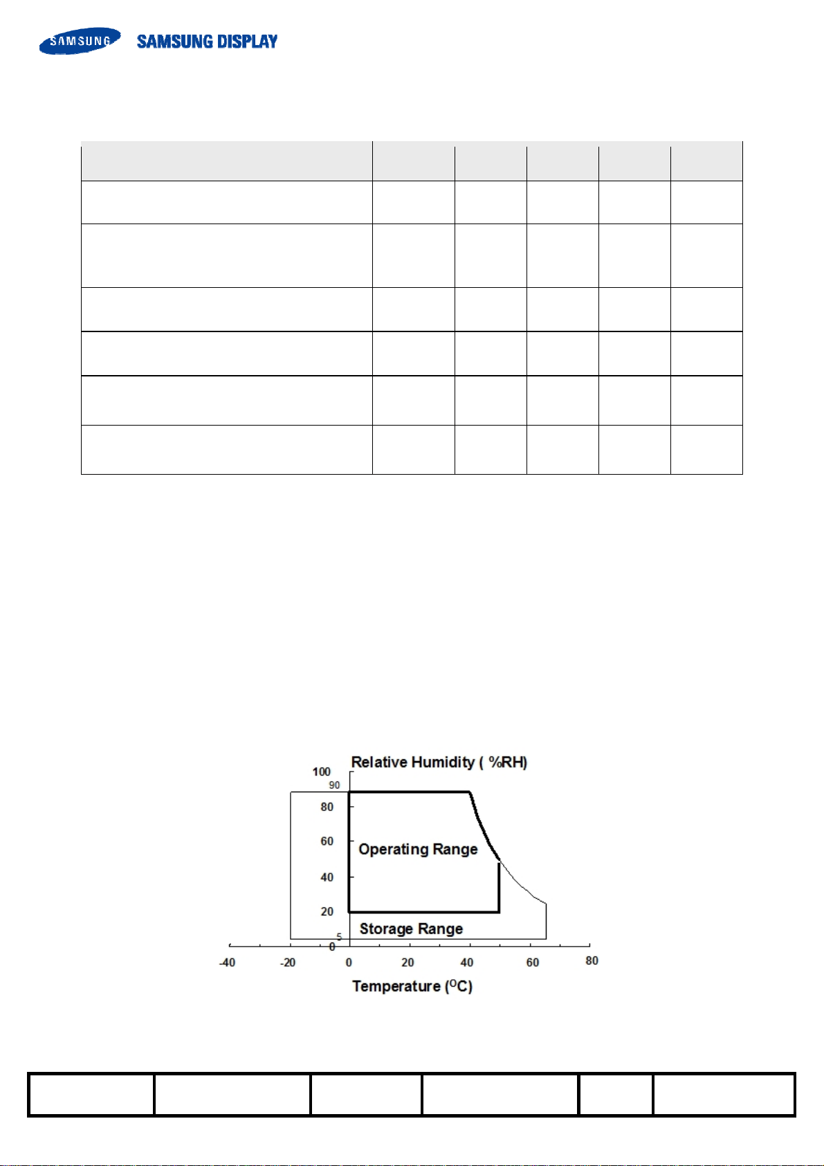
1. Absolute Maximum Ratings
If the figures on measuring instruments exceed maximum ratings, it can cause the malfunction or the
unrecoverable damage on the device.
Item Symbol Min. Max. Unit Note
T
T
H
H
V
DD
STG
OPR
STG
STG
11 13 V (1)
-20 65 ℃ (2),(4)
0 50 ℃ (2),(5)
5 90 %RH (2),(4)
20 90 %RG (2),(5)
Power supply voltage
Temperature for storage
(Temperature of glass surface)
Operating temperature
Humidity for storage
Operating humidity
Endurance on static electricity 150 V (3)
Note (1) The power supply voltage at Ta= 25 ± 2 °C
(2) Temperature and the range of relative humidity are shown in the figure below.
a. 90 % RH Max. (Ta ≤ 39 °C)
b. The relative humidity is 90% or less. (Ta >39 °C)
c. No condensation
(3) Keep the static electricity under 150V in Polarizer attaching process.
(4) Operating condition with source PCB
(5) Storage temperature condition including glass
(6) Condition without packing. (Unpacking condition)
Fig. Range for temperature and relative humidity
MODEL LSY320AN02-A Doc. No Page 5 / 45
Page 6

t
Light S
S
BLU
D6
x
x
D65
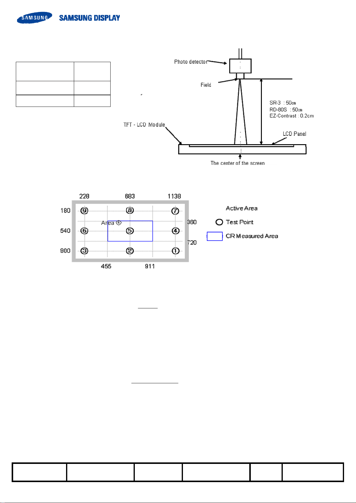
2. Optical characteristics
The optical characteristics should be measured in the dark room or the space surrounded by the similar
setting.
Measuring equipment : TOPCON RD-80S, TOPCON SR-3 ,ELDIM EZ-Contrast,
(Ta = 25 ± 2°C, VDD=12.0V, fv=60Hz, f
Item Symbol Condition Min. Typ. Max. Uni
=148.5MHz, Light source: SONY BLU (LTY320AN05-A BLU)
DCLK
ource
Note
Contrast Ratio
(At the Center of screen)
Response
time
Luminance of White
(At the Center of screen)
Transmissivity
(At the center of screen)
Color
Chromaticity
(CIE 1931)
Color Gamut - - 76 - %
Color Temperature - - 10000 - K
G-to-G
[AVE]
Red
Green
Blue
White
C/R*
Tg
Y
L
Tr 5.7 6.4
R
Ry 0.329
Gx 0.299
Gy 0.622
0.156
B
By 0.051
Wx 0.272
Wy 0.282
TPAN,SUR
=25°C
Normal
qL,R=0
qU,D=0
Viewing
Angle
3000 5000 -
- 20 30 msec
330 400 - cd/㎡
0.645
TYP.
-0.03
TYP.
+0.03
%
Sony BLU
(LTY320AN05)
ony
(LTY320AN05)
Sony BLU
(LTY320AN05)
Standard light
source
Sony BLU
(LTY320AN05)
Simulation with
Sony BLU
Spectrum
Or
5
(1)
SR-3
(3)
RD-80S
(4)
SR-3
(7)
(5),(6),(9)
SR-3
(Appendix2)
(5)
SR-3
79 89 -
79 89 -
Degree
79 89 -
79 89 -
20 %
- - 30 %
1.7 2.2 2.7
(LTY320AN05)
(LTY320AN05)
(LTY320AN05)
Sony BLU
Standard light
source
Sony BLU
Sony BLU
EZ-Contrast
Hor.
Viewing
Angle
Ver.
Transmissivity Uniformity
(9 Points)
Brightness Uniformity
(9 Points)
2Point Gamma γ
q
qR
q
qD
T
B
L
U
uni
uni
C/R≥10
7G ~ 57G
(Full = 64G)
Notice
(a) Setup for test equipment
The measurement should be executed in a stable, windless, and dark room for 40min and 60min after
operating the panel at the given temperature for stabilization of the standard light. (SDC uses the standard
luminance of the LTY320AN05-A BLU).
This measurement should be measured at the center of screen.
The environment condition: Ta = 25 ± 2 °C
(b) LTY320AN05-A BLU is consist of three diffuser sheets and LED light source.
(c) D65 Standard Light Source.
(6)
SR-3
(10)
(2)
SR-3
(8)
SR-3
The temperature of color is 6487K. The coordinate of color is Wx 0.313, Wy 0.329. The luminance of this
product is 7217.3cd/m2
MODEL LSY320AN02-A Doc. No Page 6 / 45
Page 7
−
Photo detector Field
SR-3 2°/1°
RD-80S 1°
- Definition of the test point
Note (1) Definition of contrast ratio (C/R)
: The ratio of gray max (Gmax) & gray min (Gmin) at the center point ⑤ of the panel
The measurement goes in LTY320AN05-A BLU
Gmax : The luminance with all white pixels
Gmin : The luminance with all black pixels
Note (2) Definition of the Brightness uniformity of 9 points (Test pattern : The full white)
The measurement shall be executed with the LTY320AN05-A BLU
Buni
Bmax : The maximum brightness
Bmin : The minimum brightness
CR
=∗
100
G
/
max
=
G
min
BB
(max min)
B
max
MODEL LSY320AN02-A Doc. No Page 7 / 45
Page 8
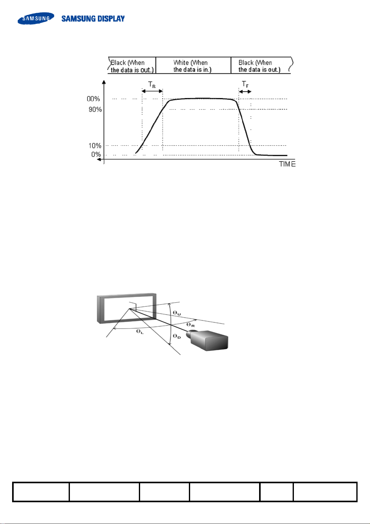
Note (3) Definition of the response time : Sum of Tr, Tf
Display data
The response
Of optical instruments
※ G-to-G : Average response time between whole gray scale to whole gray scale.
The response time is the value that was measured after it was operated in LTY320AN05-A BLU for one
hour.( at room temperature)
Note (4) The definition of luminance of white: The luminance of white at the center point ⑤
The measurement shall be executed with the LTY320AN05-A BLU.
Note (5) The definition of chromaticity (CIE 1931)
The color coordinate of red, green, blue and white at the center point ⑤
The measurement shall be executed with the LTY320AN05-A BLU.
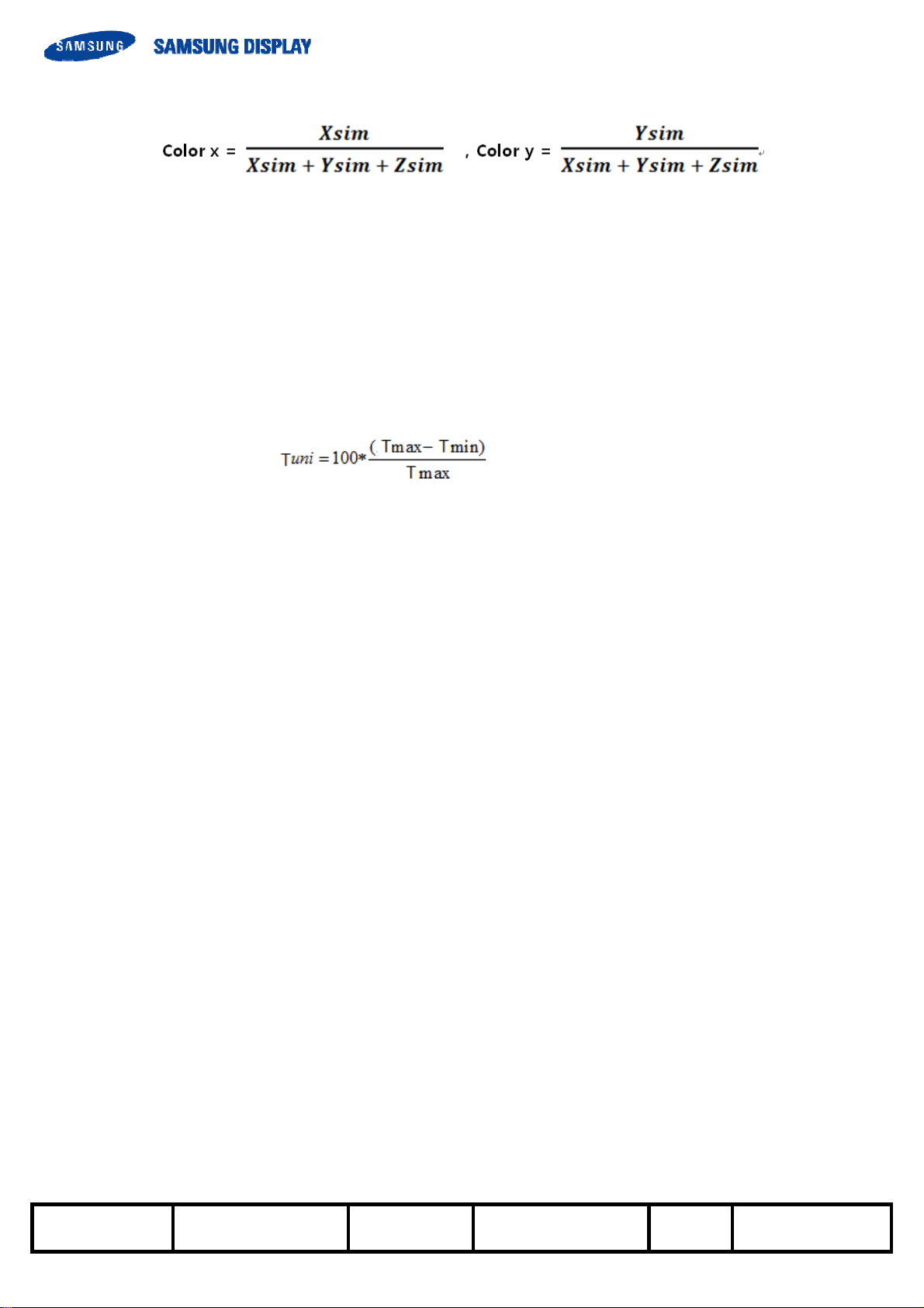
Note (6) Definition of viewing angle
: The range of viewing angle (C/R ≥10)
The measurement shall be executed with the LTY320AN05-A BLU.
Note (7) Definition of transmissivity
: The measurement shall be executed with the D65 Standard Light Source
Note (8) Definition of Gamma
Gamma X Y
XZBBB
lum
Y: Measurement Level / Z: Measurement Brightness
B
max
=
log( / ) / log( / )
=− − ×
()/( )
: Maximum Brightness / B
min max min
100 100
lum
100
: Minimum Brightness
min
MODEL LSY320AN02-A Doc. No Page 8 / 45
Page 9
Note (9) Definition of Simulation with BLU Spectrum
Simulated color Chromaticity
Xsim = Simulated Spectrum X CIE Color Matching Function x
Ysim = Simulated Spectrum X CIE Color Matching Function y
Zsim = Simulated Spectrum X CIE Color Matching Function z
Simulated Spectrum = Panel Transmittance Spectrum X Standard BLU Spectrum(Appendix2)
Note (10) Definition of the Transmissivity uniformity of 9 points
The measurement shall be executed with the D65 Standard Light Source
Tmax : The maximum transmissivity
Tmin : The minimum transmissivity
MODEL LSY320AN02-A Doc. No Page 9 / 45
Page 10
3. Electrical characteristics
3.1 TFT LCD Module
The connector for the display data & timing signal should be connected.
Ta = 25°C ± 2 °C
Item Symbol Min. Typ. Max. Unit Note
Voltage of Power Supply
(a) Black
Current
of Power
Supply
(b) White - 340 440
(c) Mosaic - 335 -
(4) Max Pattern
(V-stripe)
Vsync Frequency
Hsync Frequency
Main Frequency
Rush Current
VDD
I
DD
fV
fH
f
DCLK
I
RUSH
11 12 13 V
- 325 -
- 650 750
47 60 63
45 48.6 53
65 80 86
- - 3 A
Note (1) The ripple voltage should be controlled fewer than 10% of V
(2) fV=60Hz, fDCLK =80MHz, V
= 12.0V, DC Current.
DD
(Typ.) voltage.
DD
(1)
mA
Hz
kHz
MHz
(4)
(2),(3)
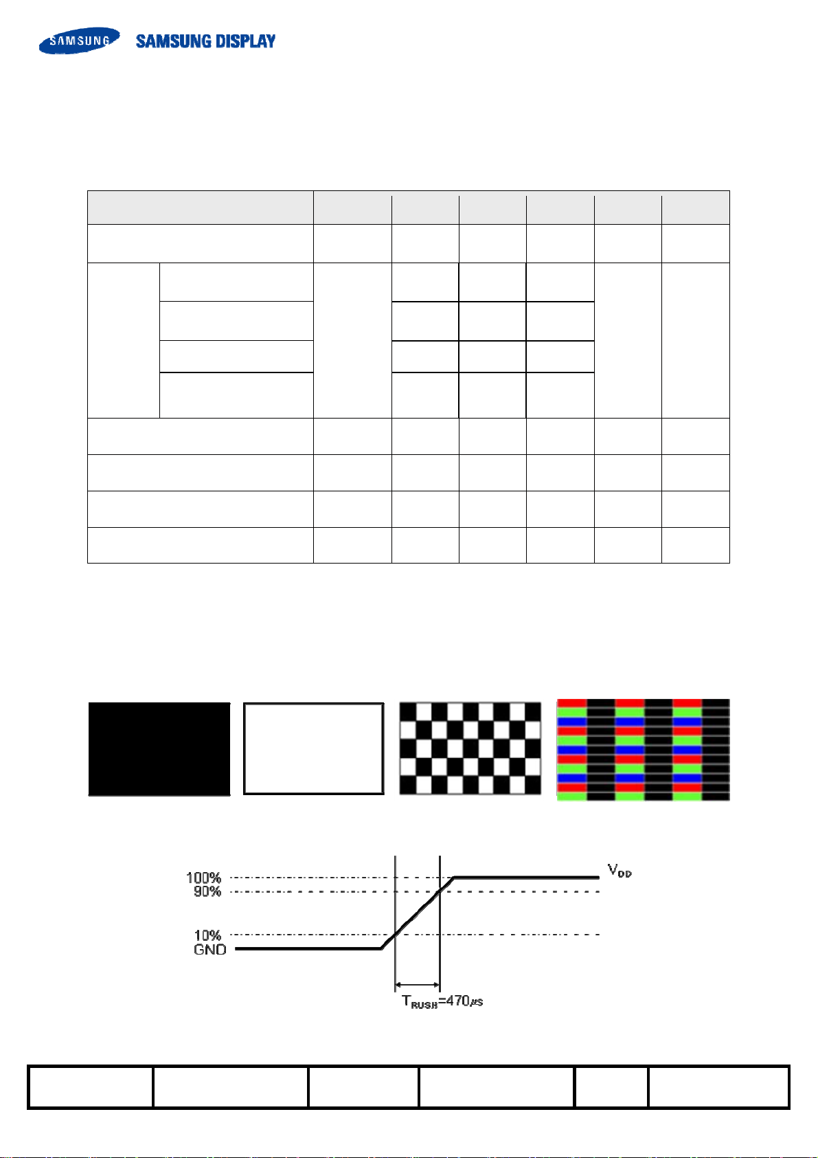
(3) Power dissipation check pattern (LCD Module only)
a) Black pattern b) White pattern c) Mosaic d) Max Pattern(V-Stripe)
(4) Conditions for measurement
The rush current, I
can be measured during T
RUSH
RUSH
is 470us
MODEL LSY320AN02-A Doc. No Page 10 / 45
Page 11
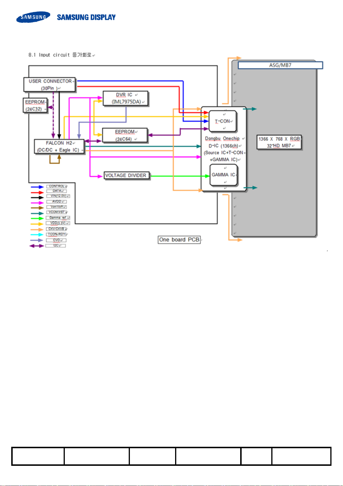
4. Block diagram
MODEL LSY320AN02-A Doc. No Page 11 / 45
Page 12
5. The Pin assignment in the input terminal
5.1. Input signal & power Connector : 196260-30041 (P-TWO Industries)
Pin Symbol Description Pin Symbol Description
1
2
3
4
5
6
7
8
9
10
11
12
NC NOTE1
SCL_I
SDA_I
GND
LV0_NI
LV0_PI
GND
LV1_NI
LV1_PI
GND
LV2_NI
LV2_PI
I2C SCL
I2C SDA
Ground
LV0_NI
LV0_PI
Ground
LV1_NI
LV1_PI
Ground
LV2_NI
LV2_PI
16 GND
17 LV3_NI
18 LV3_PI
19 GND
20
21 LVDS_SEL
22 WPN(B_INT)
23 GND
24 GND
25
26 VDD
27 VDD
NC NOTE1
NC NOTE1
Ground
LV3_NI
LV3_PI
Ground
LVDS_SEL
WPN(B_INT)
Ground
Ground
Vdd
Vdd
13
14
15
GND
LVCLK_NI
LVCLK_PI
Ground +
LVCLK_NI
LVCLK_PI
28 VDD
29 VDD
30 VDD
Note (1) No connection: These PINS are used only for the product of SAMSUNG.
(DO NOT CONNECT the input device to these pins.)
■ Option Pin Description
These pins are CMOS interface.
Please use within the range of the following restriction.
VIH:2.4V(min) / 3.5V(max)
VIL:0.0V(min) / 0.4V(max))
■SCL : Pull up 22Ω/ 4.7kΩ
■SDA : Pull up 22Ω/ 4.7kΩ
■LVDS_SEL : Pull up - Normal(VESA)
Pull down – JEIDA
Vdd
Vdd
Vdd
Note (2) WPN,SCL_I and SDA_I shouldn’t be communicated with I2C device whose output level is 5V
MODEL LSY320AN02-A Doc. No Page 12 / 45
Page 13
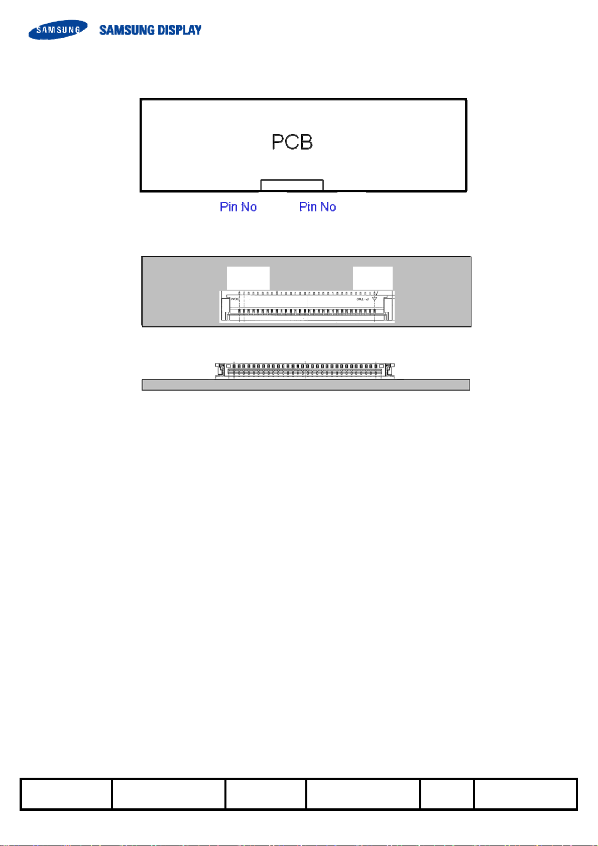
Note (3) Pin number which starts from the left side.
30
1
▼
30
#30#1
#30#1
a. Power GND pins should be connected to the LCD’s metal chassis.
b. All power input pins should be connected together.
c. All NC pins should be separated from other signal or power.
Note(4) LVDS OPTION : IF THIS PIN : LOW (GND V)/ NC → JEIDA LVDS FORMAT
OTHERWISE : HIGH (3.3V) → NORMAL NS LVDS FORMAT
MODEL LSY320AN02-A Doc. No Page 13 / 45
Page 14
5.2 LVDS Interface
- LVDS receiver : T-con (merged) ( 8Bit)
- Data format
LVDS pin JEIDA -DATA Normal-DATA
TxOUT/RxIN0
TxOUT/RxIN1
TxIN/RxOUT0 R2
TxIN/RxOUT1 R3
TxIN/RxOUT2 R4
TxIN/RxOUT3 R5
TxIN/RxOUT4 R6
TxIN/RxOUT6 R7
TxIN/RxOUT7 G2
TxIN/RxOUT8 G3
TxIN/RxOUT9 G4
TxIN/RxOUT12 G5
TxIN/RxOUT13 G6
TxIN/RxOUT14 G7
TxIN/RxOUT15 B2
R0
R1
R2
R3
R4
R5
G0
G1
G2
G3
G4
G5
B0
TxOUT/RxIN2
TxOUT/RxIN3
TxIN/RxOUT18 B3
TxIN/RxOUT19 B4
TxIN/RxOUT20 B5
TxIN/RxOUT21 B6
TxIN/RxOUT22 B7
TxIN/RxOUT24 HSYNC
TxIN/RxOUT25 VSYNC
TxIN/RxOUT26 DEN
TxIN/RxOUT27 R0
TxIN/RxOUT5 R1
TxIN/RxOUT10 G0
TxIN/RxOUT11 G1
TxIN/RxOUT16 B0
B1
B2
B3
B4
B5
HSYNC
VSYNC
DE
R6
R7
G6
G7
B6
TxIN/RxOUT17 B1
TxIN/RxOUT23 RESERVED
B7
RESERVED
MODEL LSY320AN02-A Doc. No Page 14 / 45
Page 15

5.3 Input signals, basic display colors and the gray scale of each color. (8bit))
COLOR
BASIC
COLOR
GRAY
SCALE
OF
RED
DATA SIGNAL
DISPLAY
(8bit)
R0 R1 R2 R3 R4 R5 R6 R7 G0 G1 G2 G3 G4 G5 G6 G7 B0 B1 B2 B3 B4 B5 B6 B7
BLACK 0 0 0 0 0 0 0 0 0 0 0 0 0 0 0 0 0 0 0 0 0 0 0 0 -
BLUE 0 0 0 0 0 0 0 0 0 0 0 0 0 0 0 0 1 1 1 1 1 1 1 1 -
GREEN 0 0 0 0 0 0 0 0 1 1 1 1 1 1 1 1 0 0 0 0 0 0 0 0 -
CYAN 0 0 0 0 0 0 0 0 1 1 1 1 1 1 1 1 1 1 1 1 1 1 1 1 -
RED 1 1 1 1 1 1 1 1 0 0 0 0 0 0 0 0 0 0 0 0 0 0 0 0 -
MAGENTA 1 1 1 1 1 1 1 1 0 0 0 0 0 0 0 0 1 1 1 1 1 1 1 1 -
YELLOW 1 1 1 1 1 1 1 1 1 1 1 1 1 1 1 1 0 0 0 0 0 0 0 0 -
WHITE 1 1 1 1 1 1 1 1 1 1 1 1 1 1 1 1 1 1 1 1 1 1 1 1 -
BLACK 0 0 0 0 0 0 0 0 0 0 0 0 0 0 0 0 0 0 0 0 0 0 0 0 R0
1 0 0 0 0 0 0 0 0 0 0 0 0 0 0 0 0 0 0 0 0 0 0 0 R1
DARK
↑
↓
LIGHT
0 1 0 0 0 0 0 0 0 0 0 0 0 0 0 0 0 0 0 0 0 0 0 0 R2
: : : : : : : : : : : : : : : : : :
: : : : : : : : : : : : : : : : : :
1 0 1 1 1 1 1 1 0 0 0 0 0 0 0 0 0 0 0 0 0 0 0 0 R253
0 1 1 1 1 1 1 1 0 0 0 0 0 0 0 0 0 0 0 0 0 0 0 0 R254
RED GREEN BLUE
GRAY
SCALE
LEVEL
R3~
R252
GRAY
SCALE
OF
GREEN
GRAY
SCALE
OF
BLUE
RED 1 1 1 1 1 1 1 1 0 0 0 0 0 0 0 0 0 0 0 0 0 0 0 0 R255
BLACK 0 0 0 0 0 0 0 0 0 0 0 0 0 0 0 0 0 0 0 0 0 0 0 0 G0
0 0 0 0 0 0 0 0 1 0 0 0 0 0 0 0 0 0 0 0 0 0 0 0 G1
DARK
↑
↓
LIGHT
GREEN 0 0 0 0 0 0 0 0 1 1 1 1 1 1 1 1 0 0 0 0 0 0 0 0 G255
BLACK 0 0 0 0 0 0 0 0 0 0 0 0 0 0 0 0 0 0 0 0 0 0 0 0 B0
DARK
↑
↓
LIGHT
BLUE 0 0 0 0 0 0 0 0 0 0 0 0 0 0 0 0 1 1 1 1 1 1 1 1 B255
0 0 0 0 0 0 0 0 0 1 0 0 0 0 0 0 0 0 0 0 0 0 0 0 G2
: : : : : : : : : : : : : : : : : :
: : : : : : : : : : : : : : : : : :
0 0 0 0 0 0 0 0 1 0 1 1 1 1 1 1 0 0 0 0 0 0 0 0 G253
0 0 0 0 0 0 0 0 0 1 1 1 1 1 1 1 0 0 0 0 0 0 0 0 G254
0 0 0 0 0 0 0 0 0 0 0 0 0 0 0 0 1 0 0 0 0 0 0 0 B1
0 0 0 0 0 0 0 0 0 0 0 0 0 0 0 0 0 1 0 0 0 0 0 0 B2
: : : : : : : : : : : : : : : : : :
: : : : : : : : : : : : : : : : : :
0 0 0 0 0 0 0 0 0 0 0 0 0 0 0 0 1 0 1 1 1 1 1 1 B253
0 0 0 0 0 0 0 0 0 0 0 0 0 0 0 0 0 1 1 1 1 1 1 1 B254
G3~
G252
B3~
B252
Note) The definition of gray :
Rn : Red gray, Gn : Green gray, Bn : Blue gray (n = Gray level)
Input signal : 0 = Low level voltage, 1 = High level voltage
MODEL LSY320AN02-A Doc. No Page 15 / 45
Page 16

6. Interface timing
6.1 The parameters of timing ( Only DE mode )
SIGNAL ITEM SMBOL MIN. TYP. MAX. Unit NOTE
Clock
Hsync
Vsync
Term for the
vertical
display
Term for the
horizontal
display
Frequency
Active
display
period
Total vertical
Active
display
period
Horizontal
Total
1/T
F
F
T
T
T
T
VD
HD
C
H
V
V
H
65 80 86 MHz -
45
47 60 63 Hz -
- 768 - Lines -
775 810 1300 Lines -
- 1366 - Clocks -
1450 1648 2000 clocks -
48.6
53
KHz
-
Note) These products don’t have to receive the signal of Hsync & Vsync from the input device.
(1) Key points when testing: TTL controls the signal and the CLK at the input terminal of LVDS Tx of the system.
(2) Internal VDD = 3.3V
(3) Spread spectrum
- The limit of spread spectrum's range of SET in which the LCD module is assembled should be within ± 3 %.
MODEL LSY320AN02-A Doc. No Page 16 / 45
Page 17

6.2 Timing diagrams of interface signal (Only DE mode )
MODEL LSY320AN02-A Doc. No Page 17 / 45
Page 18

6.3 Characteristics of Input data of LVDS
(1) DC Specification
(2) AC Specification
MODEL LSY320AN02-A Doc. No Page 18 / 45
Page 19

6.4 The sequence of power on and off
To prevent a latch-up phenomena or the DC operation of the LCD Module, the power on/off sequence should
be accorded with the settings described in the diagram below.
The supply voltage of the external system for the Module input should be the same as the definition of V
Apply the lamp voltage within the LCD operation range. When the back light turns on before the LCD
operation or the LCD turns off before the back light turns off, the display may momentarily show abnormal
screen.
In case of V
= off level, please keep the level of input signals low or keep a high impedance.
DD
T4 should be measured after the Module has been fully discharged between power off and on period.
Interface signal should not be kept at high impedance when the power is on.
While the V
is off level, please keep the level of input signals low or keep a high impedance condition.
DD
The figure of T4 should be measured after the module has been fully discharged between the periods
when the power is on and off.
6.5 Input spread spectrum specification.
*SET Vender should check waterfall before apply spread spectrum which occurs based on modulation
frequency.
DD
.
MODEL LSY320AN02-A Doc. No Page 19 / 45
Page 20

7. Outline dimension
7.1 The adhesive size of POL
The next figure shows the size of POL on the drawing sheet attached to the panel for BLU design.
<Figure.>
The POL size of CF : 710.7 X 405.6 mm LEFT&RIGHT ± 0.5mm,
The POL size of TFT: 710.7 X 405.6 mm LEFT&RIGHT ± 0.5mm,
The total adhesion allowance of POL is ± 1.15mm
7.2 The drawing sheet for the size of the OLB bonding
MODEL LSY320AN02-A Doc. No Page 20 / 45
Page 21

A
A
8. Reliability test
8.1 Panel
Item Test Condition Quantity Note
HTOL 60 ℃ (Panel change 500hr / circuit change 250hr) 8
LTOL -5 ℃ (Panel change 500hr / circuit change 250hr) 4
THB 50 ℃ / 90 %RH(Panel change 500hr / circuit change 250hr) 10
SG
Low
temperature
SG
High
Temperature
Image sticking
Decompressio
n
HTS 70 ℃, Storage (Panel change 500hr / circuit change 250hr) 4
LTS -25 ℃, Storage(Panel change 500hr / circuit change 250hr) 4
Max. frequency 25℃~-40℃
Min. frequency 60℃operation 96hr
25 ℃ / Mosaic pattern(9*10) 12hrs
Rolling pattern 12hrs / 3cycles
-40~50℃, 0m(0ft) ~ 13,700m(45,000ft), 72.5Hr 4
Each
Cell
Each
Cell
8
ASG Product Only
ASG Product Only
Transportation
condition
WHTS 60 ℃ / 75 %RH , Storage ,500HR 4
Noise Electromagnetic noise: Overall 23dB 이하 2
Complex
stress
ESD S-IC Input ±7KV, Output ±4KV 3
EOS (optional)
drop(20cm) → temperature/humidity(-30~60℃ / 40℃ 90%RH)
→ pressure → vibration(5~200Hz 1.05Grms, 2hr) → drop(20cm)
-20℃~60℃, 0~90%RH, 2cycle 4
Item Test condition
Vin Input
step
Signal Input
step
Surge combination (High impedance)
Pass Condition: 5kV under
Surge combination (High impedance)
Pass Condition: 120V under
1pallet
2
[ Criteria on evaluation]
There should be no change of the product, which may affect to the practical display functions, when the
display quality test is executed under the normal operation setting.
* HTOL/ LTOL : The operating cycle on the high and low temperature
* THB : Temperature humidity slant
* HTS/LTS : The storage at the high and low temperature
* WHTS : The storage in the high temperature with the high humidity
MODEL LSY320AN02-A Doc. No Page 21 / 45
Page 22

9. General precautions
9.1 Handling
(a) When the panel kit and BLU kit are assembled, the panel kit and BLU kit should be attached to the
set system firmly by combining each mounted holes. Be careful not to give the mechanical stress.
(b) Be careful not to give any extra mechanical stress to the panel when designing the set, and BLU kit.
(c) Be cautious not to give any strong mechanical shock and / or any forces to the panel kit.
Applying the any forces to the panel may cause the abnormal operation or the damage to the panel
kit and the back light unit kit.
(d) Refrain from applying any forces to the source PBA and the drive IC in the process of the handling
or installing to the set. If any forces are applied to the products, it may cause damage or a
malfunction in the panel kit.
(e) Refrain from applying any forces which cause a constant shock to the back side of panel kit, the set
design and BLU kit. If any forces are applied to the products, it may cause an abnormal display, a
functional failure and etc.
(f) Note that polarizer could be damaged easily.
Do not press or scratch the bare surface with the material which is harder than a HB pencil lead.
(g) Wipe off water droplets or oil immediately. If you leave the droplets for a long time on the product, a
staining or the discoloration may occur.
(h) If the surface of the polarizer is dirty, clean it using the absorbent cotton or the soft cloth.
(i) Desirable cleaners are water or IPA (Isopropyl Alcohol).
Do not use Kenton type materials (ex. Acetone), Ethyl alcohol, Toluene, Ethyl acid or Methyl chloride.
These might cause the permanent damage to the polarizer due to chemical reaction.
(j) If the liquid crystal material leaks from the panel, this should be kept away from the eyes or mouth.
If this contacts to hands, legs, or clothes, you must washed it away with soap thoroughly and see a
doctor for the medical examination.
(k) Protect the panel kit and BLU Kit out of the static electricity. Otherwise the circuit IC could be
damaged.
- Reference : Process control standard of SDC
No. Item Control standard
1 Ionizer All Equipment should be controlled under 150V.(Typ. 100V)
2 Carrying Roller Carrying Roller should be controlled under 200V.
Equipment Ground
3
Resistance
All Equipment Ground Should be less than 1ohm.
MODEL LSY320AN02-A Doc. No Page 22 / 45
Page 23

(l) Remove the stains with finger-stalls wearing soft gloves in order to keep the display clean in the
process of the incoming inspection and the assembly process.
(m) Do not pull or fold the source drive IC which connects to the source PBA and the panel or the gate
drive IC.
(n) Do not pull, fold or bend the source drive IC and the gate drive IC in any processes.
If not, the source drive IC could be bent one time in the process of assembling the panel Kit and the
BLU Kit.
(o) Do not adjust the variable resistor located on the panel kit and BLU kit except when adjusting the
flicker.
(p) Do not touch the pins of the interface connector directly with bare hands.
(q) Be cautious not to be peeled off the protection film.
- Make sure to peel off slowly
(It is recommended to peel it off at the speed of more than 8sec.
constantly.)
- The peeling direction is shown at the Fig
- Instruct the ground worker to work with the adequate methods
such as the antistatic wrist band.
- Maker sure to be grounded the source PBA while peeling of the
protection film.
- Ionized air should be blown over during the peeling
- The protection film should not t be contacted to the source drive
IC.
- If the adhesive stains remain on the polarizer after the
protection film is peeled off, please move stains with isopropyl-
alcohol liquid.
(r) The protection film for the polarizer on the panel kit should be slowly peeled off just before using so
that the electrostatic charge can be minimized.
(s) The panel kit and BLU kit have high frequency circuits. The sufficient suppression to the EMI should
be done by the set manufacturers.
(t) The set of which the panel is assembled shall not be twisted. If the product is twisted, it may cause
the damage on the product.
(u) Surface Temp. of IC should be controlled less than 100℃, operating over the Temp. can cause the
damage or decrease of lifetime.
MODEL LSY320AN02-A Doc. No Page 23 / 45
Page 24

9.2 Storage
The storage condition for packing (Not included transportation)
ITEM Unit Min. Max.
Storage
(℃)
Temperature
Storage
(%rH)
Humidity
Storage life 6 months
(1) The storage room should provide good ventilation and temperature control.
(2) Products should not be placed on the floor, but on the Pallet away from a wall.
(3) Prevent products from direct sunlight, moisture nor water; Be cautious of a buildup of
condensation.
Storage
Condition
(4) Avoid other hazardous environment while storing goods.
(5) If products delivered or kept in conditions of the recommended temperature or humidity,
we recommend you leave them at a circumstance which is shown in the following table.
period 1 month 2 months 3 months 4 months 5 months 6 months
Baking
50℃, 10%
No Baking
Condition
24Hr
50℃, 10%, 48Hr
9.3 Operation
(a) Do not connect or disconnect the FFC cable during the "Power On" condition.
(b) Power supply should be always turned on and off by the "Power on/off sequence"
(c) The module has high frequency circuits. The sufficient suppression to the electromagnetic interference
should be done by the system manufacturers. The grounding and shielding methods is important to
minimize the interference.
(d) The cables between TV SET connector and Control PBA interface cable should be connected directly
to have a minimized length. A longer cable between TV SET connector and Control PBA interface
cable maybe operate abnormal display
(e) Recommend to age for over 1 hour at least in the state, which the product is driving initially to stabilize
the characteristic of the initial TFT.
(f) Response time depends on the temperature.( In Lower temperature, it becomes longer)
MODEL LSY320AN02-A Doc. No Page 24 / 45
Page 25

9.4 Operation condition guide
(a) The LCD product shall be operated under normal conditions.
The normal condition is defined as below;
- Temperature : 20±15℃
- Humidity : 55±20%
- Display pattern : continually changing pattern (Not stationary)
(b) If the product will be used under extreme conditions such as under the high temperature, humidity,
display patterns or the operation time etc.., it is strongly recommended to contact SDC for the
advice about the application of engineering . Otherwise, its reliability and the function may not be
guaranteed. Extreme conditions are commonly found at airports, transit stations, banks, stock
markets, and controlling systems.
9.5 Others
(a) The ultra-violet ray filter is necessary for the outdoor operation.
(b) Avoid the condensation of water which may result in the improper operation of product or the
disconnection of electrode.
(c) Do not exceed the limit on the absolute maximum rating. (For example, the supply voltage
variation, the input voltage variation, the variation in content of parts and environmental
temperature, and so on) If not, panel may be damaged.
(d) If the module keeps displaying the same pattern for a long period of time, the image may be
remained to the screen. To avoid the image sticking, it is recommended to use a screen saver.
(e) This Panel has its circuitry of PCB's on the rear side, so it should be handled carefully in order for a
force not to be applied.
(f) Please contact the SDC in advance when the same pattern is displayed for a long time
MODEL LSY320AN02-A Doc. No Page 25 / 45
Page 26

r
10. Special precautions
10.1 Lists to be cautious when executing the design process
No. Component Expected cause
Upholding part for
1
2
3
4
5 Drive IC
6 Drive IC
7
panel
The shape of the
upholding part for
panel
The edge of
upholding part for
panel
Upholding part for
panel
IC
component
Prevent the panel from breaking by assigning gaps between the panel and the upholding part for panel on the drawing
for the upholding part for panel.
Refer to the (a), (b), (c) of 3-1 for the design of BLU.
Design the upholding part for panel to fit to the panel appropriately when designing the BLU since the shape of the
upholding part for panel may damage the panel.
Refer to the (a), (b), (c) of 3-1 for the design of BLU.
Design the edge of panel to have a sufficient space with the upholding part for panel when designing the BLU since the
edge of the upholding part for panel may damage the panel when assembling the panel and BLU.
Refer to the (a), (b), (c) of 3-1 for the design of BLU.
Place the upholding part for the panel in order for the shape of mold, which contacts with the panel not to interfere with
the area of panel.
Refer to the (a), (b), (c) of 3-1 for the design of BLU.
Design the BLU in order for the COF not to contain the lead crack resulted from the tensioned COF created when the
product is twisted if the space between the D-IC COF and the middle mold isn't sufficient.
Refer to the (a), (b), (c),(d),(e),(f), and (g)of 3-2 for the design of BLU.
Design the BLU in order for the product not to contain the lead crack resulted from the tensioned COF caused under the
condition, which the product is twisted by fixing the source PCB.
Refer to the (a), (b), (c),(d),(e),(f), and (g)of 3-2 for the design of BLU.
1) The temperature of each part of product suggested by our company and the second vendor shall meet the standard
of temperature, which is recommended not to be exceeded by our company when the product is affected under the
various temperature ranges.
Apply over 1mm long separation distance stated in the safety standard between the electric part and each conductor.
(Apply the rated separation distance when insulating.)
8 Thermal pad
9 POL
10 PBA
11 Circuit
The height of
12
component
Between the FFC
13
and the C-PBA
14 Panel
15 Aging
The attachment of
16
17 Drive IC
18
19 S-PBA
gasket
The prohibited
bandwidth
Apply the thermal pad in a designated size to the product as a measure to lower the temperature of heat in order for
each part to use the rated temperature.
The surrounding area of the POL shall be treated with an electrification treatment since the external ESD may cause a
phenomenon, which the POL is coming off.
In addition, the GND portion of source PBA shall be grounded.
The GND portion of each PBA shall be contacted with the GND portion of BLU.
Refer to the (a) and (b) of 3-3 for the design of BLU.
The standardized approval from the client is required since the EMI is executed by a client.
Our company can only measure the reference since the client measures the BLU.
Design the BLU with considering the maximum height of parts, which our company suggests.
Design the instrument with considering the length between the FFC and the control PBA.
(The marginal minimum length of 5mm or 8mm is required.)
The surface temperature of panel shall be maintained within 0℃ and 45℃ when the external ambient temperature is at
25℃. (Design the BLU with considering the increase of the temperature in the panel by the LED, CCFL, and etc.)
Recommend to age for over 1 hour at least in the state, which the product is driving initially to stabilize the characteristic
of the initial TFT.
The additional confirmation by our company is required If the attachment of gasket to the S-PBA of our company is
required.(To fix the S-PBA or the EMI)
Design the top chassis and the driver IC to be contacted by placing the shape of emboss inside the top chassis as a
measure to prevent the driver IC from heating. The size of emboss shall be designed in larger size than the size of IC
inside the film of the driver IC.
Refer to the (a), (b), (c),(d),(e),(f), and (g)of 3-2 for the design of BLU.
Design the BLU in order for the BLU not to interfere with the area, where the control PBA and the sou
located densely according to the drawing for the BLU from our company.
The material, which contacts with the bottom side of S-PBA which has a pattern shall be non-conducting material or
shall be insulated.
ce PBA are
MODEL LSY320AN02-A Doc. No Page 26 / 45
Page 27

11. EDID Information
11.1 EEPROM Data Format
No Item Spec Address Data Remark
1 Panel Product Vender HDLCD 000 00
EEPROM Data
SONY
Choice
- Note 1
2 Screen Size 32 001 20
3 H-Resolution 1366 002,003 05,56
4 V-Resolution 768 004,005 03,00
5 Vertical Frequency 50/60Hz 006 00 - Note 2
6 Data Format 8bit 007 01 - Note 3
7 FRC Revision Information
8 Part Number
st
1
LSY320AN
0210
0ED 00
0E0~0EB
4C,53,59,33,32,30,
41,4E,30,32,31,30
Note1) Note2) Note3)
Data Panel Vender Code
00 HDLCD(SEC)
Data V-Frequency
00 50/60Hz
Data Data Format
00 6Bit
01 Others
01 100/120HZ
01 8Bit
16
Hexadecimal
16
Hexadecimal
16
Hexadecimal
ASCII
- Note 4
ASCII
- Note 5, 6
02 Others
02 200/240Hz
02 10Bit
03 Others
04 Others
05 Others
Note4) FRC Revision Code will be Changed from “00” to “41” (A) When FRC IC is changed.
At First MP. This Code will be “00”
Note 5) LSY[Z]XXXXXXX Only for SDC Model
Note 6) Rest of them must be “00” (Null)
MODEL LSY320AN02-A Doc. No Page 27 / 45
Page 28

11.2 EEPROM Data Table
0 1 2 3 4 5 6 7 8 9 A B C D E F
0 00 20 05 56 03 00 00 01
00 00 00 00 00 00 00 00 00 00 00 00 00 00 00 00
1
00 00 00 00 00 00 00 00 00 00 00 00 00 00 00 00
2
00 00 00 00 00 00 00 00 00 00 00 00 00 00 00 00
3
00 00 00 00 00 00 00 00 00 00 00 00 00 00 00 00
4
00 00 00 00 00 00 00 00 00 00 00 00 00 00 00 00
5
00 00 00 00 00 00 00 00 00 00 00 00 00 00 00 00
6
00 00 00 00 00 00 00 00 00 00 00 00 00 00 00 00
7
00 00 00 00 00 00 00 00 00 00 00 00 00 00 00 00
8
00 00 00 00
00 00 00 00
00 00 00 00 00 00 00 00 00 00 00 00 00 00 00 00
9
00 00 00 00 00 00 00 00 00 00 00 00 00 00 00 00
A
00 00 00 00 00 00 00 00 00 00 00 00 00 00 00 00
B
00 00 00 00 00 00 00 00 00 00 00 00 00 00 00 00
C
00 00 00 00 00 00 00 00 00 00 00 00 00 00 00 00
D
00
E 4C 53 59 33 32 30 41 4E 30 32 31 30
00 00 00 00 00 00 00 00 00 00 00 00 00 00 00 00
F
00 00 00
Note) EDID Data are written in Sub address 0000h ~ 00FFh.
Other area (Sub address 0100h ~ 0FFFh) of EEPROM data are managed by Sony.
MODEL LSY320AN02-A Doc. No Page 28 / 45
Page 29

Appendix1
Reference of each Panel size
MODEL LSY320AN02-A Doc. No Page 29 / 45
Page 30

1. Amount of beveling of panel
A
2. Cross Section of cell
0.7 ± 0.040 mm
C/F
TFT
Protector film included
0.253 ± 0.040 mm
0.248 ± 0.040 mm
Protector film included
MODEL LSY320AN02-A Doc. No Page 30 / 45
Page 31

3. Source PCB
MODEL LSY320AN02-A Doc. No Page 31 / 45
Page 32

4. FFC Cable
MODEL LSY320AN02-A Doc. No Page 32 / 45
Page 33

Appendix2
Spectrum Data of SONY BLU
(LTY320AN05-A)
MODEL LSY320AN02-A Doc. No Page 33 / 45
Page 34

1. Spectrum Data of SONY BLU (LTY320AN05-A)
WL(nm) Watts/sr/msr WL(nm) Watts/sr/msr WL(nm) Watts/sr/msr WL(nm) Watts/sr/msr WL(nm) Watts/sr/msr
380
381
382
383
384
385
386
387
388
389
390
391
392
393
394
395
396
397
398
399
400
401
402
403
404
405
406
407
408
409
410
411
412
413
414
415
416
417
418
419
420
421
422
423
424
425
426
427
428
429
6.12E-03
6.62E-03
6.05E-03
6.05E-03
5.51E-03
5.44E-03
4.65E-03
4.21E-03
3.78E-03
3.72E-03
3.14E-03
2.79E-03
2.54E-03
2.34E-03
2.20E-03
1.96E-03
1.82E-03
1.73E-03
1.58E-03
1.54E-03
1.49E-03
1.53E-03
1.48E-03
1.58E-03
1.64E-03
1.82E-03
2.01E-03
2.35E-03
2.58E-03
2.99E-03
3.57E-03
4.28E-03
5.01E-03
6.03E-03
7.26E-03
8.72E-03
1.06E-02
1.28E-02
1.56E-02
1.89E-02
2.27E-02
2.72E-02
3.28E-02
3.90E-02
4.65E-02
5.47E-02
6.48E-02
7.62E-02
8.94E-02
1.03E-01
430
431
432
433
434
435
436
437
438
439
440
441
442
443
444
445
446
447
448
449
450
451
452
453
454
455
456
457
458
459
460
461
462
463
464
465
466
467
468
469
470
471
472
473
474
475
476
477
478
479
1.20E-01
1.38E-01
1.60E-01
1.81E-01
2.07E-01
2.33E-01
2.61E-01
2.91E-01
3.25E-01
3.56E-01
3.85E-01
4.14E-01
4.33E-01
4.53E-01
4.61E-01
4.58E-01
4.50E-01
4.36E-01
4.14E-01
3.87E-01
3.57E-01
3.29E-01
2.98E-01
2.70E-01
2.47E-01
2.22E-01
2.03E-01
1.85E-01
1.69E-01
1.55E-01
1.42E-01
1.29E-01
1.18E-01
1.07E-01
9.61E-02
8.64E-02
7.78E-02
6.97E-02
6.28E-02
5.66E-02
5.09E-02
4.62E-02
4.18E-02
3.81E-02
3.49E-02
3.20E-02
2.92E-02
2.67E-02
2.45E-02
2.26E-02
480
481
482
483
484
485
486
487
488
489
490
491
492
493
494
495
496
497
498
499
500
501
502
503
504
505
506
507
508
509
510
511
512
513
514
515
516
517
518
519
520
521
522
523
524
525
526
527
528
529
2.07E-02
1.90E-02
1.76E-02
1.63E-02
1.52E-02
1.42E-02
1.35E-02
1.30E-02
1.26E-02
1.23E-02
1.21E-02
1.21E-02
1.23E-02
1.26E-02
1.31E-02
1.36E-02
1.44E-02
1.54E-02
1.64E-02
1.78E-02
1.93E-02
2.09E-02
2.28E-02
2.48E-02
2.69E-02
2.95E-02
3.21E-02
3.50E-02
3.82E-02
4.14E-02
4.48E-02
4.83E-02
5.21E-02
5.61E-02
6.01E-02
6.42E-02
6.81E-02
7.21E-02
7.57E-02
7.97E-02
8.36E-02
8.74E-02
9.12E-02
9.50E-02
9.85E-02
1.02E-01
1.06E-01
1.10E-01
1.13E-01
1.16E-01
530
531
532
533
534
535
536
537
538
539
540
541
542
543
544
545
546
547
548
549
550
551
552
553
554
555
556
557
558
559
560
561
562
563
564
565
566
567
568
569
570
571
572
573
574
575
576
577
578
579
1.18E-01
1.20E-01
1.22E-01
1.23E-01
1.24E-01
1.26E-01
1.27E-01
1.28E-01
1.28E-01
1.29E-01
1.29E-01
1.29E-01
1.29E-01
1.28E-01
1.28E-01
1.27E-01
1.26E-01
1.25E-01
1.24E-01
1.22E-01
1.21E-01
1.20E-01
1.19E-01
1.17E-01
1.16E-01
1.14E-01
1.13E-01
1.11E-01
1.09E-01
1.08E-01
1.06E-01
1.04E-01
1.03E-01
1.02E-01
1.00E-01
9.87E-02
9.73E-02
9.60E-02
9.45E-02
9.32E-02
9.19E-02
9.07E-02
8.94E-02
8.83E-02
8.74E-02
8.64E-02
8.56E-02
8.48E-02
8.39E-02
8.31E-02
580
581
582
583
584
585
586
587
588
589
590
591
592
593
594
595
596
597
598
599
600
601
602
603
604
605
606
607
608
609
610
611
612
613
614
615
616
617
618
619
620
621
622
623
624
625
626
627
628
629
< 380nm ~ 629nm >
8.24E-02
8.17E-02
8.12E-02
8.05E-02
8.02E-02
7.97E-02
7.92E-02
7.86E-02
7.82E-02
7.80E-02
7.78E-02
7.77E-02
7.72E-02
7.71E-02
7.70E-02
7.69E-02
7.64E-02
7.65E-02
7.63E-02
7.61E-02
7.60E-02
7.59E-02
7.58E-02
7.54E-02
7.54E-02
7.53E-02
7.49E-02
7.48E-02
7.45E-02
7.41E-02
7.41E-02
7.36E-02
7.33E-02
7.31E-02
7.26E-02
7.23E-02
7.19E-02
7.15E-02
7.11E-02
7.05E-02
7.03E-02
6.97E-02
6.92E-02
6.87E-02
6.84E-02
6.78E-02
6.73E-02
6.69E-02
6.62E-02
6.56E-02
MODEL LSY320AN02-A Doc. No Page 34 / 45
Page 35

WL(nm) Watts/sr/msr WL(nm) Watts/sr/msr WL(nm) Watts/sr/msr WL(nm) Watts/sr/msr
630
631
632
633
634
635
636
637
638
639
640
641
642
643
644
645
646
647
648
649
650
651
652
653
654
655
656
657
658
659
660
661
662
663
664
665
666
667
668
669
670
671
672
673
674
675
676
677
678
679
6.51E-02
6.48E-02
6.41E-02
6.35E-02
6.30E-02
6.25E-02
6.20E-02
6.12E-02
6.05E-02
5.98E-02
5.91E-02
5.83E-02
5.74E-02
5.67E-02
5.60E-02
5.51E-02
5.45E-02
5.36E-02
5.28E-02
5.21E-02
5.13E-02
5.04E-02
4.96E-02
4.87E-02
4.79E-02
4.69E-02
4.61E-02
4.53E-02
4.44E-02
4.36E-02
4.28E-02
4.19E-02
4.09E-02
4.01E-02
3.93E-02
3.84E-02
3.76E-02
3.68E-02
3.60E-02
3.52E-02
3.44E-02
3.36E-02
3.29E-02
3.21E-02
3.14E-02
3.07E-02
3.01E-02
2.93E-02
2.86E-02
2.80E-02
680
681
682
683
684
685
686
687
688
689
690
691
692
693
694
695
696
697
698
699
700
701
702
703
704
705
706
707
708
709
710
711
712
713
714
715
716
717
718
719
720
721
722
723
724
725
726
727
728
729
2.73E-02
2.66E-02
2.60E-02
2.53E-02
2.46E-02
2.40E-02
2.34E-02
2.28E-02
2.23E-02
2.17E-02
2.11E-02
2.06E-02
2.00E-02
1.95E-02
1.90E-02
1.85E-02
1.80E-02
1.74E-02
1.68E-02
1.64E-02
1.58E-02
1.54E-02
1.49E-02
1.44E-02
1.40E-02
1.36E-02
1.32E-02
1.28E-02
1.24E-02
1.20E-02
1.16E-02
1.13E-02
1.09E-02
1.05E-02
1.01E-02
9.81E-03
9.46E-03
9.11E-03
8.78E-03
8.47E-03
8.14E-03
7.81E-03
7.53E-03
7.22E-03
6.94E-03
6.66E-03
6.40E-03
6.18E-03
5.95E-03
5.71E-03
730
731
732
733
734
735
736
737
738
739
740
741
742
743
744
745
746
747
748
749
750
751
752
753
754
755
756
757
758
759
760
761
762
763
764
765
766
767
768
769
770
771
772
773
774
775
776
777
778
779
5.49E-03
5.32E-03
5.14E-03
5.02E-03
4.85E-03
4.72E-03
4.57E-03
4.46E-03
4.36E-03
4.24E-03
4.13E-03
4.05E-03
3.97E-03
3.89E-03
3.79E-03
3.72E-03
3.64E-03
3.56E-03
3.49E-03
3.41E-03
3.35E-03
3.29E-03
3.22E-03
3.14E-03
3.06E-03
2.99E-03
2.92E-03
2.86E-03
2.77E-03
2.72E-03
2.65E-03
2.57E-03
2.49E-03
2.45E-03
2.37E-03
2.30E-03
2.22E-03
2.17E-03
2.12E-03
2.06E-03
1.98E-03
1.93E-03
1.89E-03
1.82E-03
1.77E-03
1.71E-03
1.67E-03
1.61E-03
1.57E-03
1.52E-03
780 1.48E-03
< 630nm ~ 780nm >
Spectrum data
MODEL LSY320AN02-A Doc. No Page 35 / 45
Page 36

Appendix3
Driver IC ESD Specification
MODEL LSY320AN02-A Doc. No Page 36 / 45
Page 37

1. D-IC ESD Specification
D-IC FFC PIN INPUT D-IC Ouput
DB7501 ±7kV ±4kV
MODEL LSY320AN02-A Doc. No Page 37 / 45
Page 38

Appendix4
Packing Information
MODEL LSY320AN02-A Doc. No Page 38 / 45
Page 39

1. Panel Kit Packing
Dimension Weight Q’ty / PLT Total Weight
Item
W x L x H (mm) g pcs Kg
Packing Tray 894 x 634 x 112 968 20
Pallet 1150 x 1270 x 125 18080 1
Panel
-
Tray Top 894 x 634 x 40 620 2
1200 200
292.4
Cushion Pad 717 x 452.3 x 2.5 26 220
Silica gel - 40 80
Paper Box 908 x 1282 x 1045 4845 1
Stack Layer max 2 Pallet
Total Size 1150 x 1282 x 1170 -
NOTE) The Cushion PAD is worked out for antistatic device.
MODEL LSY320AN02-A Doc. No Page 39 / 45
Page 40

2. Panel Kit Marking & Others
A nameplate bearing followed by is affixed to a shipped product at the specified
location on each product.
(1) Cell Label
MODEL LSY320AN02-A Doc. No Page 40 / 45
Page 41

(2) Tray Label
A
LSY320AN02
AXX
(3) Box Label
LSY320AN02
XX
200
MODEL LSY320AN02-A Doc. No Page 41 / 45
Page 42

Appendix5
Mechanical Information
MODEL LSY320AN02-A Doc. No Page 42 / 45
Page 43

1. Mechanical Information
Item
Cell size
(TFT glass)
Cell size
(CF glass)
Polarizer size
(TFT side)
Polarizer size
(CF side)
Specification
unit Notes
Min Typ Max
H - 713.0 -
mm
V - 410.5 -
T 660 700 740 μm
H - 713.0 -
mm
V - 408.2 -
T 660 700 740 μm
H 710.20 710.70 711.20
mm
V 405.10 405.60 406.10
T 208 248 288 μm
H 710.20 710.70 711.20
mm
V 405.10 405.60 406.10
T 213 253 293 μm
Surface hardness of
polarizer
Warp of Cell Ass’y -1 +1 mm (1)
2H - -
Note (1) Measurement Method
a. Measurement Timing : After OLB Process at SDC Line
b. Measure a gap on surface plate by using thickness gauge.
Measure 4point(a,b,c,d) as Fig 1.
MODEL LSY320AN02-A Doc. No Page 43 / 45
Page 44

Appendix6
Caution
MODEL LSY320AN02-A Doc. No Page 44 / 45
Page 45

(1) When using BLU PWM(Pulse Width Modulation), PWM frequency is recommended to be 1.5 times of
Frame Frequency(Fv) for preventing waterfall phenomenon.
(2) SDC recommends that operating time as open-cell should not over 10min and during operating, D-IC’s Tj
shouldn’t be over 125℃.
MODEL LSY320AN02-A Doc. No Page 45 / 45
 Loading...