

Page 1
SEC CODE
VD사업부
승 인 서
Ver.
품명
(Description)
규격
(Specification)
LCD-Panel
55inch, FHD, 120Hz
Maker P/N LSC550HJ02-
적용기종
(적용모델)
특기사항
기안
(DRAWING)
심사
(CHECK)
합의
(AGREEMENT)
승인
(APPROVAL)
2011. . 2011. . 2011. . 2011. .
승인기간 승인일로부터
Maker
ADDRESS
URL http://www.samsungdisplay.com
MODEL LSC550HJ02 Doc. No 07-000-S-120104 Page
삼성디스플레이
336-841 충남 아산시 탕정면 명암리 200번지
Tel. 041-535-1114
1/28
Page 2
Approval Spec.
Customer :Visual Display Division DATE : 4. Jan. 2012
MODEL:LSC550HJ02
Any Modification of Specification is not allowed without SDC's Permission.
APPROVED BY
Customer’s Approval
SIGNATURE
DATE
PREPARED BY
4. Jan. 2011
4. Jan. 2011
Samsung Display Co . , LTD.
MODEL LSC550HJ02 Doc. No 07-000-S-120104 Page
DATE
DATE
2/28
Page 3
Contents
Revision History -------------------------------------------------------------------------------------------- (4)
General Description --------------------------------------------------------------------------------------- (5)
General Information --------------------------------------------------------------------------------------- (5)
1. Absolute Maximum Ratings -------------------------------------------------------------------------- (6)
2. Optical Characteristics --------------------------------------------------------------------------------- (7)
3. Electrical Characteristics ------------------------------------------------------------------------------ (10)
3.1 TFT LCD Module
4. Block Diagram ------------------------------------------------------------------------------------------- (11)
5. Input Terminal Pin Assignment --------------------------------------------------------------------- (12)
5.1. Input Signal & Power
5.2 LVDS Interface
5.3 Input Signals, Basic Display Colors and Gray Scale of Each Color
6. Interface Timing ---------------------------------------------------------------------------------------- (16)
6.1 Timing Parameters
6.2 Timing Diagrams of interface Signal
6.3 Power ON/OFF Sequence
7. Outline Dimension -------------------------------------------------------------------------------------- (19)
8. Reliability Test ------------------------------------------------------------------------------------------- (20)
9. Packing --------------------------------------------------------------------------------------------------(21)
9.1 CARTON(Internal Package)
9.2 Packing Specification
9.3 Middle Sheet Specification
9.4 Middle Sheet Outline Dimension
10. Marking & Others ------------------------------------------------------------------------------------- (23)
11. General Precaution ----------------------------------------------------------------------------------- (25)
11.1 Handling
11.2 Storage
11.3 Operation
11.4 Operation Condition Guide
11.5 Others
MODEL LSC550HJ02 Doc. No 07-000-S-120104 Page
3/28
Page 4
Revision History
Date Rev. No Page Summary
9.Nov.2011
22.Dec.2011
22.Dec.2011
22.Dec.2011
22.Dec.2011
27.Dec.2011
28.Dec.2011
4.Jan.2012
000 all First issued
001 5 Display Colors 10bit 8bit
002 10 TFT LCD Module
003 16 Interface Parameter
004 16 Frame Frequency
005 7 Transmittance
006 7 Color Chromaticity (CIE 1931) Ry 0.340 0.330
007 27 Storage Condition
MODEL LSC550HJ02 Doc. No 07-000-S-120104 Page
4/28
Page 5
General Description
Description
LSC550HJ02 is a color active matrix liquid crystal display(LCD) that uses amorphous
silicon TFT( Thin Film Transistor) as switching components. This model is composed of a
TFT LCD panel, a driver circuit. The resolution of a 55“ is 1920 x 1080 and this model can
display up to 16.7 million colors with wide viewing angle of 89° or higher in all directions.
This panel is intended to support applications to provide a excellent performance for Flat
Panel Display such as Home-alone Multimedia TFT-LCD TV and High Definition TV.
Features
High contrast & aperture ratio with wide color gamut
SVA (Super Vertical Align) mode
Wide viewing angle (±178°)
High speed response
FHD resolution (16:9)
4Ch LVDS (Low Voltage Differential Signaling) interface
General Information
Items Specification Unit Note
1227.6(H) x 700.5(V)
Panel Size
1.76(D)
Weight 3.15(Max) kg
Pixel Pitch 0.210(H) X 0.630(V) mm
Active Display Area 1209.6(H) X 680.4(V) mm
Surface Treatment Haze 2%, Hard-coating (2H)
Display Colors 16.7M (8Bits Dithering) colors
Number of Pixels 1920 x 1080 pixel
Pixel Arrangement RGB vertical stripe
Display Mode Normally Black
±1.0mm
mm
Max
MODEL LSC550HJ02 Doc. No 07-000-S-120104 Page
5/28
Page 6
1. Absolute Maximum Ratings
If the condition exceeds maximum ratings, it can cause malfunction or unrecoverable
damage to the device.
(VSS = 0 V)
Item Symbol Min. Max. Unit Note
Power Supply Voltage V
Storage temperature T
DD
STG
10.8 13.2 V (1)
-20 65
Glass surface
temperature
Center T
OPR
0 50
(Operation)
Note (1) Ta= 25 ± 2 °C
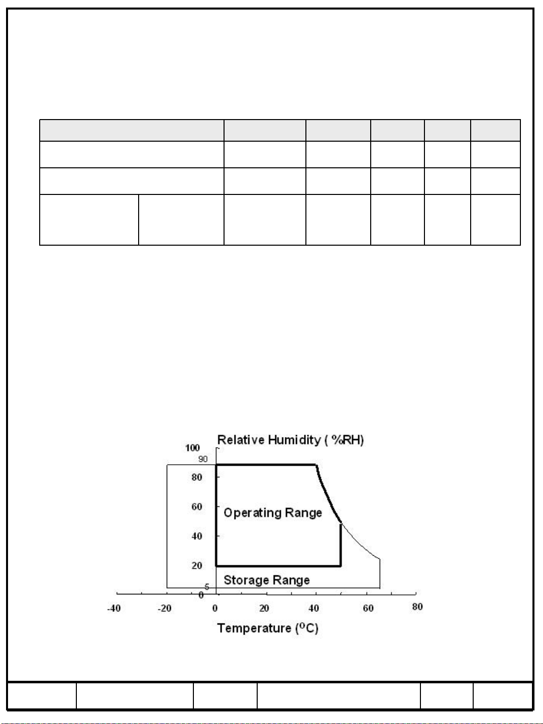
(2) Temperature and relative humidity range are shown in the figure below.
a. 90 % RH Max. (Ta ≤ 39 °C)
b. Relative Humidity is 90% or less. (Ta > 39 °C)
c. No condensation
℃
℃
(2)
(2)
MODEL LSC550HJ02 Doc. No 07-000-S-120104 Page
6/28
Page 7
2. Optical Characteristics
The optical characteristics should be measured in a dark room or equivalent.
Measuring equipment : D65,RD-80S,EZ-Contrast
(Ta = 25 ± 2°C, VDD=12V)
Item Symbol Condition Min. Typ. Max. Unit Note
Contrast Ratio
(Center of screen)
Response
Time
Transmittance T 6.045 6.5 - %
Color
Chromaticity
(CIE 1931)
sRGB Concordance - - 98.5 - %
Color Temperature - - 10,000 - K
Viewing
Angle
Transmittance
Uniformity
(9 Points)
G-to-G Tg - 8 15 msec
Red
Green
Blue
White
Hor.
Ver.
C/R
Normal
Rx
Ry 0.330
Gx 0.300
Gy 0.600
Bx 0.150
By 0.060
Wx 0.280
Wy 0.290
q
L
q
R
q
U
q
D
T
uni
qL,R=0
qU,D=0
Viewing
Angle
C/R≥10
3,000 5,000 -
0.640
TYP.
-0.03
75 89 75 89 75 89 75 89 -
- -
TYP.
+0.03
Degree
10
%
(1)
D65
(3)
RD-80S
(4)
D65
(5),(6)
D65
(5)
D65
(6)
EZ-
Contrast
(2)
D65
Notice
(a) Test Equipment Setup
The measurement should be executed in a stable, windless and dark room between
40min and 60min after operating the Panel at the given temperature for stabilization
of the standard light(SEC use standard illuminant D65 Media).
This should be measured in the center of screen. Environment condition : Ta = 25 ± 2 °C
(b) D65 Media means general available light source.
Color Temperature is 6504K , a color coordinate is Wx 0.2948, Wy 0.322,
Luminance is 3389cd/㎡
MODEL LSC550HJ02 Doc. No 07-000-S-120104 Page
7/28
Page 8
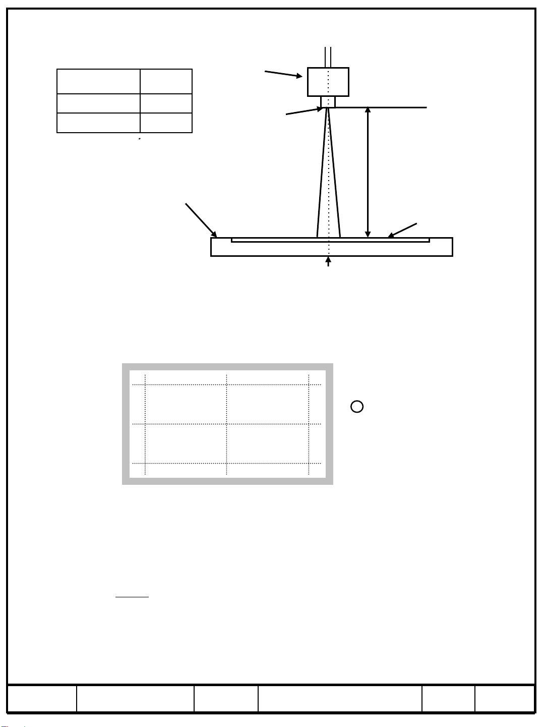
Photo detector Field
Photo detector
SR3
RD-80S
TFT - LCD Module
- Definition of test point
320 960 1600
180
⑨
1°
2°
⑧
Field
The center of the screen
⑦
BM-5A : 50㎝
RD-80S : 50㎝
EZ-Contrast:0㎝
LCD Panel
Active Area
Test Point
540
900
Note (1) Definition of Contrast Ratio (C/R)
: Ratio of gray max (Gmax) & gray min (Gmin) at the center point ⑤ of the panel
: The measurement goes in D65 Standard Light Source
/
C R
⑥
⑤ ④
②③
max
G
min
G
Gmax : Luminance with all pixels white
Gmin : Luminance with all pixels black
①
MODEL LSC550HJ02 Doc. No 07-000-S-120104 Page
8/28
Page 9
Note (2) Definition of 9 points Transmittance uniformity (Test pattern : Full White)
The measurement goes in D65 Standard Light Source
T T
Tuni
( max min)
T
max
100
Tmax : Maximum Transmittance
Tmin : Minimum Transmittance
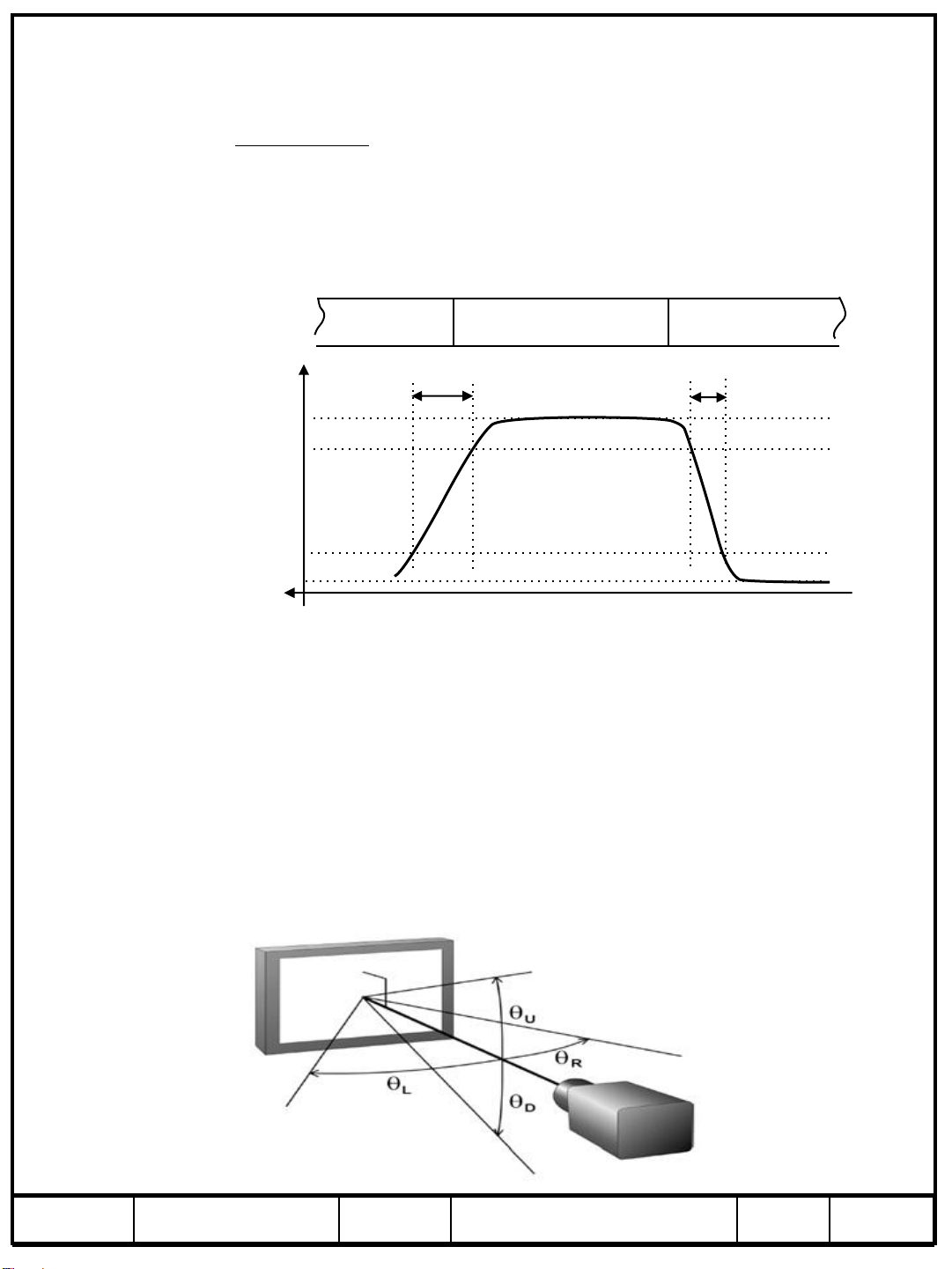
Note (3) Definition of Response time : Sum of Tr, Tf
Display data
Optical Instruments
Response
100%
Black (data off)
T
R
White (data on)
90%
10%
0%
※ G-to-G : Average response time between Gray to Gray (Scale)
Note (4) Definition of Transmittance : Transmittance at center point ⑤
The measurement goes in D65 Standard Light Source
Note (5) Definition of Color Chromaticity (CIE 1931)
Color coordinate of Red, Green, Blue & White at center point ⑤
The measurement goes in D65 Standard Light Source
Black (data off)
T
F
TIME
Note (6) Definition of Viewing Angle
: Viewing angle range (C/R ≥10)
The measurement goes in D65 Standard Light Source
MODEL LSC550HJ02 Doc. No 07-000-S-120104 Page
9/28
Page 10

3. Electrical Characteristics
3.1 TFT LCD Module
The connector for display data & timing signal should be connected.
Ta = 25°C ± 2 °C
Item Symbol Min. Typ. Max. Unit Note
Voltage of Power Supply VDD 10.8 12.0 13.2 V (1)
Current
of Power
Supply
(a) Black
IDD
(c) N-pattern - 1700 1800 mA
- 1100 1200 mA
(2),(3)(b) White - 1100 1200 mA
Vsync Frequency fV - 60 - Hz
Hsync Frequency fH - 67.5 - kHz
Main Frequency Fdclk - 148.5 - MHz
Rush Current IRUSH - 4 6 A (4)
Note (1) The ripple voltage should be controlled under 10% of VDD.
(2) fV= 120 Hz, fDCLK = 297 MHz, VDD= 12.0V, DC Current.
(3) Power dissipation check pattern (LCD Module only)
a) Black Pattern b) White Pattern c) N-pattern
(4) Measurement Conditions
V
100%
DD
90%
10%
GND
T
=470㎲
RUSH
Rush Current I
can be measured when T
RUSH
. is 470㎲.
RUSH
MODEL LSC550HJ02 Doc. No 07-000-S-120104 Page
10/28
Page 11

4. Block Diagram
S
Control PCB
(149*75,4L)
I2C
Vin
LVDS 4Ch
10bit input
Vin
MERGE IC
(Gamma/DVR/OPAMP/
RESET/I2C Analog S/W)
EEPROM
TCON
3.3V
(AVDD/hAVDD/VSS1/V
SS2/VDD3.3/VDD1.2/V
LDO
DC/DC IC
ONE/Scan driver)
1.8V
1.2V
Push-
Pull
Gamma
Aipi ++ signal
Control Signal
Aipi ++ signal
Control Signal
AVDD
1.2V / AVDD/ ASG Scan
hAVDD / VSS1/ VSS2
Vcom
O
U
R
C
E
P
C
B
4L
68 Pin
68 Pin
S
O
U
R
C
E
P
C
B
MB3 ASG2
SOURCE IC
MB4 966Ch,
AP++
3EA
PANEL : 1920 x 1080 , RD
SOURCE IC
MB4 966Ch,
AP++
3EA
4L
MODEL LSC550HJ02 Doc. No 07-000-S-120104 Page
MB3 ASG2
11/28
Page 12

5. Input Terminal Pin Assignment
5.1. Input Signal & Power
Pin Description Pin Description
1 Vdd (12V) 26
2 Vdd (12V) 27 Rx4[1]N
3 Vdd (12V) 28 Rx4[1]P
4 Vdd (12V) 29 Rx4[2]N
5 Vdd (12V) 30 Rx4[2]P
6 N.C 31 GND
7 GND 32 Rx4CLK8 GND 33 Rx4CLK+
9 GND 34 GND
10
11 Rx2[0]P 36 Rx4[3]P
12 Rx2[1]N 37 Rx4[4]N NOTE3
13 Rx2[1]P 38 Rx4[4]P NOTE3
14 Rx2[2]N 39 GND
15 Rx2[2]P 40 No connection
16 GND 41 No connection
17 Rx2CLK- 42 No connection
18 Rx2CLK+ 43 No connection
19 GND 44 No connection
20 Rx2[3]N 45 LVDS_SEL NOTE2
21 Rx2[3]P 46 No connection
22 Rx2[4]N NOTE3 47 No connection
23 Rx2[4]P NOTE3 48 No connection
24 GND 49 No connection
25 Even LVDS Rx4[0]N 50 No connection
Even
LVDS
Signal
Rx2[0]N 35 Rx4[3]N
51 No connection
Even
LVDS
Signal
Rx4[0]P
NOTE1
NOTE1
Note 1) NOT CONNECTED : THIS PINS ARE ONLY USED FOR SEC INTERNAL OPERATIONS.
Note 2) LVDS OPTION : IF THIS PIN : HIGH (3.3 V) → NORMAL NS LVDS FORMAT
OTHERWISE : LOW (GND) OR OPEN(NC) → JEIDA LVDS FORMAT
Note 3) IF LVDS 8Bit Input
MODEL LSC550HJ02 Doc. No 07-000-S-120104 Page
12/28
Page 13

Note(1) Pin number starts from Bottom side
PCB
▼
#1
#1 #8
#8
#1 #51
▼
#1
#51
Fig. Connector diagram
a. Power GND pins should be connected to the LCD’s metal chassis.
b. All power input pins should be connected together.
c. All NC pin should be separated from other signal or power.
MODEL LSC550HJ02 Doc. No 07-000-S-120104 Page
13/28
Page 14

5.2 LVDS Interface
- LVDS Receiver : Tcon (merged) - Data Format (JEIDA)
LVDS pin JEIDA -DATA
TxIN/RxOUT0 R2
TxIN/RxOUT1 R3
TxIN/RxOUT2 R4
TxOUT/RxIN0
TxOUT/RxIN1
TxOUT/RxIN2
TxIN/RxOUT3 R5
TxIN/RxOUT4 R6
TxIN/RxOUT6 R7
TxIN/RxOUT7 G2
TxIN/RxOUT8 G3
TxIN/RxOUT9 G4
TxIN/RxOUT12 G5
TxIN/RxOUT13 G6
TxIN/RxOUT14 G7
TxIN/RxOUT15 B2
TxIN/RxOUT18 B3
TxIN/RxOUT19 B4
TxIN/RxOUT20 B5
TxIN/RxOUT21 B6
TxIN/RxOUT22 B7
TxIN/RxOUT24 HSYNC
TxIN/RxOUT25 VSYNC
TxIN/RxOUT26 DEN
TxIN/RxOUT27 R0
TxIN/RxOUT5 R1
TxIN/RxOUT10 G0
TxOUT/RxIN3
TxIN/RxOUT11 G1
TxIN/RxOUT16 B0
TxIN/RxOUT17 B1
TxIN/RxOUT23 RESERVED
MODEL LSC550HJ02 Doc. No 07-000-S-120104 Page
14/28
Page 15
5.3 Input Signals, Basic Display Colors and Gray Scale of Each Color
COLOR
BASIC
COLOR
GRAY
SCALE
OF
RED
DATA SIGNAL
DISPLAY
(8bit)
R0 R1 R2 R3 R4 R5 R6 R7 R8 R9 G0 G1 G2 G3 G4 G5 G6 G7 G8 G9 B0 B1 B2 B3 B4 B5 B6 B7 B8 B9
BLACK 0 0 0 0 0 0 0 0 0 0 0 0 0 0 0 0 0 0 0 0 0 0 0 0 0 0 0 0 0 0 -
BLUE 0 0 0 0 0 0 0 0 0 0 0 0 0 0 0 0 0 0 0 0 1 1 1 1 1 1 1 1 1 1 -
GREEN 0 0 0 0 0 0 0 0 0 0 1 1 1 1 1 1 1 1 1 1 0 0 0 0 0 0 0 0 0 0 -
CYAN 0 0 0 0 0 0 0 0 0 0 1 1 1 1 1 1 1 1 1 1 1 1 1 1 1 1 1 1 1 1 -
RED 1 1 1 1 1 1 1 1 1 1 0 0 0 0 0 0 0 0 0 0 0 0 0 0 0 0 0 0 0 0 -
MAGENTA 1 1 1 1 1 1 1 1 1 1 0 0 0 0 0 0 0 0 0 0 1 1 1 1 1 1 1 1 1 1 -
YELLOW 1 1 1 1 1 1 1 1 1 1 1 1 1 1 1 1 1 1 1 1 0 0 0 0 0 0 0 0 0 0 -
WHITE 1 1 1 1 1 1 1 1 1 1 1 1 1 1 1 1 1 1 1 1 1 1 1 1 1 1 1 1 1 1 BLACK 0 0 0 0 0 0 0 0 0 0 0 0 0 0 0 0 0 0 0 0 0 0 0 0 0 0 0 0 0 0 R0
1 0 0 0 0 0 0 0 0 0 0 0 0 0 0 0 0 0 0 0 0 0 0 0 0 0 0 0 0 0 R1
DARK
LIGHT
RED 1 1 1 1 1 1 1 1 1 1 0 0 0 0 0 0 0 0 0 0 0 0 0 0 0 0 0 0 0 0 R1023
0 1 0 0 0 0 0 0 0 0 0 0 0 0 0 0 0 0 0 0 0 0 0 0 0 0 0 0 0 0 R2
↑
: : : : : : : : : : : : : : : : : : : : : : : : : : : : : :
: : : : : : : : : : : : : : : : : : : : : : : : : : : : : :
↓
1 0 1 1 1 1 1 1 1 1 0 0 0 0 0 0 0 0 0 0 0 0 0 0 0 0 0 0 0 0 R1021
0 1 1 1 1 1 1 1 1 1 0 0 0 0 0 0 0 0 0 0 0 0 0 0 0 0 0 0 0 0 R1022
RED GREEN BLUE
GRAY
SCALE
LEVEL
R1020
R3~
BLACK 0 0 0 0 0 0 0 0 0 0 0 0 0 0 0 0 0 0 0 0 0 0 0 0 0 0 0 0 0 0 G0
0 0 0 0 0 0 0 0 0 0 1 0 0 0 0 0 0 0 0 0 0 0 0 0 0 0 0 0 0 0 G1
GRAY
DARK
SCALE
OF
GREEN
LIGHT
GREEN 0 0 0 0 0 0 0 0 0 0 1 1 1 1 1 1 1 1 1 1 0 0 0 0 0 0 0 0 0 0 G1023
BLACK 0 0 0 0 0 0 0 0 0 0 0 0 0 0 0 0 0 0 0 0 0 0 0 0 0 0 0 0 0 0 B0
DARK
GRAY
SCALE
OF
BLUE
LIGHT
BLUE 0 0 0 0 0 0 0 0 0 0 0 0 0 0 0 0 0 0 0 0 1 1 1 1 1 1 1 1 1 1 B1023
0 0 0 0 0 0 0 0 0 0 0 1 0 0 0 0 0 0 0 0 0 0 0 0 0 0 0 0 0 0 G2
↑
: : : : : : : : : : : : : : : : : : : : : : : : : : : : : :
: : : : : : : : : : : : : : : : : : : : : : : : : : : : : :
↓
0 0 0 0 0 0 0 0 0 0 1 0 1 1 1 1 1 1 1 1 0 0 0 0 0 0 0 0 0 0 G1021
0 0 0 0 0 0 0 0 0 0 0 1 1 1 1 1 1 1 1 1 0 0 0 0 0 0 0 0 0 0 G1022
0 0 0 0 0 0 0 0 0 0 0 0 0 0 0 0 0 0 0 0 1 0 0 0 0 0 0 0 0 0 B1
0 0 0 0 0 0 0 0 0 0 0 0 0 0 0 0 0 0 0 0 0 1 0 0 0 0 0 0 0 0 B2
↑
: : : : : : : : : : : : : : : : : : : : : : : : : : : : : :
: : : : : : : : : : : : : : : : : : : : : : : : : : : : : :
↓
0 0 0 0 0 0 0 0 0 0 0 0 0 0 0 0 0 0 0 0 1 0 1 1 1 1 1 1 1 1 B1021
0 0 0 0 0 0 0 0 0 0 0 0 0 0 0 0 0 0 0 0 0 1 1 1 1 1 1 1 1 1 B1022
Note) Definition of Gray :
Rn : Red Gray, Gn : Green Gray, Bn : Blue Gray (n = Gray level)
Input Signal : 0 = Low level voltage, 1 = High level voltage
G3~
G1020
B3~
B1020
MODEL LSC550HJ02 Doc. No 07-000-S-120104 Page
15/28
Page 16

6. Interface Timing
6.1 Timing Parameters ( Timing-Controller )
SIGNAL ITEM SYMBOL MIN. TYP. MAX. Unit NOTE
Clock Frequency 1/T
Frame
Frequency
Cycle
Active
Display
Vertical
Period
Display Term
Vertical
Total
Active
Display
Horizontal
Period
Display Term
Horizontal
Total
C
T
V
T
H
T
VD
T
VB
T
HD
T
H
260 297 305
95 120 125
120 135 140 Khz
- 1080 -
1110 1185 1350
- 1920 -
2092 2120 2596
MHz
Hz
Lines
Lines
Clocks
clocks
Note) This product is DE only mode. The input of Hsync & Vsync signal does
not have an effect on normal operation.
(1) Test Point : TTL control signal and CLK at LVDS Tx input terminal in system
(2) Internal VDD = 3.3V
(3) Spread spectrum
- Modulation rate (max) : ± 1.5 %
- Modulation Frequency : 30 ~ 300KHz
MODEL LSC550HJ02 Doc. No 07-000-S-120104 Page
16/28
Page 17

6.2 Timing diagrams of interface signal ( DE only mode )
TV
TVD
DE
TH
THD
DE
DCLK
TC
DATA
SIGNALS
MODEL LSC550HJ02 Doc. No 07-000-S-120104 Page
17/28
Page 18

6.3 Power ON/OFF Sequence
To prevent a latch-up or DC operation of the LCD Module, the power on/off
sequence should be as the diagram below.
0.5ms<T1≤10ms
1ms<T2≤50ms
0ms<T3≤50ms
1000ms≤T4
1000ms≤T5
100ms≤T6
T1 : VDDrising time from 10% to 90%
T2 : The time from VDDto valid data at power ON.
T3 : The time from valid data off to VDDoff at power Off.
T4 : VDDoff time for Windows restart
T5 : The time from valid data to B/L enable at power ON.
T6 : The time from valid data off to B/L disable at power Off.
The supply voltage of the external system for the Module input should be the same
as the definition of VDD.
Apply the lamp voltage within the LCD operation range. When the back light turns on
before the LCD operation or the LCD turns off before the back light turns off,
the display may momentarily show abnormal screen.
In case of VDD= off level,
please keep the level of input signals low or keep a high impedance.
T4 should be measured after the Module has been fully discharged between power off
and on period.
Interface signal should not be kept at high impedance when the power is on.
MODEL LSC550HJ02 Doc. No 07-000-S-120104 Page
18/28
Page 19

7. Outline Dimension
BM Tolerance Spec.
- Real BM Width spec. : ±0.1mm
- Gap between Active Center and BM
up/down/right/left : ±0.1mm (a,a’)
MODEL LSC550HJ02 Doc. No 07-000-S-120104 Page
19/28
Page 20

8. Reliability Test
Item Test condition Quantity
HTOL
HTOL2
LTOL
THB
Temperature
Humidity
Stress
Image Sticking
Altitude
50℃ / 500HR
60℃ / 500HR
-5℃ / 500HR
50℃ / 90%RH / 500HR
-20℃~65℃, 0~90%RH, 2cycle / 194HR
25℃ / Mosaic pattern(9*10) 12hrs
Rolling pattern 12hrs / 3cycles / 72HR
-40℃~50℃, 0m(oft) ~ 13,700m(45,000ft) / 72.5HR
4EA
4EA
4EA
4EA
4EA
4EA
4EA
Open Cell
Complex Test
ESD
[ Result Evaluation Criteria]
Under the display quality test conditions with normal operation state, these should
be no change which may affect practical display functions.
* HTOL/ LTOL : High/Low Temperature Operating Life
** THB : Temperature Humidity Bias
*** HTS/LTS : High/Low Temperature Storage
**** WHTS : Wet High Temperature Storage
MODEL LSC550HJ02 Doc. No 07-000-S-120104 Page
WHTS / HTS / LTS / TRAY FALL / 600HR
Input : ±7kV / Output : ±4kV / 1Time, 1Point
10EA
4EA
20/28
Page 21

9. PACKING
9.1 CARTON (Internal Package)
(1) Packing Form Corrugated fiberboard box and corrugated cardboard as shock absorber
(2) Packing Method
Packing- Upper Box
Pallet Tray
10EA
Pallet-Plastic
9.2 Packing Specification
ITEM Specification Remark
1. 3.35 Kg / LCD (15[ea]/Tray, 150[ea]/Pallet)
LCD Packing 150ea / Box
2. 0.04 Kg / Middle sheet (18[ea]/Tray, 180[ea]/Pallet)
3. 3.04 Kg / Panel tray (10ea/Pallet)
4. 1.82 Kg / Packing Box (1ea)
15EA
Pallet-Wood 1Box / Pallet
Pallet size H x V x height 1,360mm(H) x 940mm(V) x 1,205mm(height)
Pallet weight 566.42 kg
1. Pallet weight = 21 kg
2. 21 Kg / Pallet
Pallet(21kg) + Panel tray(30.4kg) + Panel(502.5kg)
+ Middle sheet(7.2Kg) + Packing Box (5.32kg)
MODEL LSC550HJ02 Doc. No 07-000-S-120104 Page
21/28
Page 22

9.3 Middle Sheet Specification
ITEM Specification
Temperature
Measurement Condition
Humidity 20% ~ 60%
Material Polyethylene
Surface Resistance 106 ~ 10
Static
(No Friction)
Frictional Voltage
Dynamic
(Friction : 5times at once)
9.4 Middle Sheet Outline Dimension
9.9
Ω
Less than 200V
Less than 500V
25℃
MODEL LSC550HJ02 Doc. No 07-000-S-120104 Page
22/28
Page 23

10. MARKING & OTHERS
A nameplate bearing followed by is affixed to a shipped product at the specified
location on each product.
(1) Cell Label
LSC550HJ02
Lot number : X X X X XXX XX X
Cell Position No. (In the Glass)
Glass No. (In the one Lot)
Lot No. (Glass)
Month
Year (Note1)
Product code
Line
MODEL LSC550HJ02 Doc. No 07-000-S-120104 Page
23/28
Page 24

(2) Box Label
LSC550HJ02
xxxx
150
MODEL LSC550HJ02 Doc. No 07-000-S-120104 Page
24/28
Page 25

11. General Precautions
11.1 Handling
(a) When the Module is assembled, it should be attached to the system firmly
using all mounting holes. Be careful not to twist and bend the Module.
(b) Refrain from strong mechanical shock and / or any force to the Module.
In addition to damage, this may cause improper operation or damage to the Module
and CCFL back light.
(c) Note that polarizers are very fragile and could be damage easily.
Do not press or scratch the surface harder than a HB pencil lead.
(d) Wipe off water droplets or oil immediately. If you leave the droplets for a long
time, staining or discoloration may occur.
(e) If the surface of the polarizer is dirty, clean it using absorbent cotton or soft cloth.
(f) Desirable cleaners are water, IPA(Isopropyl Alcohol) or Hexane.
Do not use Ketone type materials(ex. Acetone), Ethyl alcohol, Toluene, Ethyl acid
or Methyl chloride. It might permanent damage to the polarizer due to chemical
reaction.
(g) If the liquid crystal material leaks from the panel, it should be kept away
from the eyes or mouth . In case of contact with hands, legs or clothes, it must
be washed away with soap thoroughly.
(h) Protect the module from Electrostatic discharge. Otherwise the ASIC IC or
Semiconductor would be damaged.
(i) Use finger-stalls with soft gloves in order to keep display clean during the
incoming inspection and assembly process.
(k) Protection film for polarizer on the Module should be slowly peeled off just before use
so that the electrostatic charge can be minimized. Must put on antistatic glove while
handle a module
(l) Pins of I/F connector should not be touched directly with bare hands.
MODEL LSC550HJ02 Doc. No 07-000-S-120104 Page
25/28
Page 26

* Process Control Standard
Item Management standard value and performance standard
1 Anti-static mat (shelf) 1 to 50 [Mohm]
2
3 Ionizer
4 Anti-static wrist band 0.8 to 10 [Mohm]
5
6 Temperature
7 Humidity 60 to 70 [%RH]
Anti-static mat (floor,
desk)
Anti-static wrist band
entry and ground
resistance
1 to 100 [Mohm]
Attenuate from ± 1,000V to ± 100V within 2 sec
Below 1,000 [ohm]
0 ∼ 35℃
MODEL LSC550HJ02 Doc. No 07-000-S-120104 Page
26/28
Page 27

11.2 Storage
We highly recommend to comply with the criteria in the table below
ITEM Unit Min. Max.
Storage
Temperature
Storage
Humidity
Storage life 6 months
- The storage room should provide good ventilation and temperature control.
- Products should not be placed on the floor, but on the Pallet away from
- Prevent products from direct sunlight, moisture nor water; Be cautious of
Storage
Condition
- Avoid other hazardous environment while storing goods.
(℃) 5 40
(%rH) 35 75
a wall.
a build up of condensation.
After 1 month 2 month 3 month 4month 5 month 6month
Baking No backing 50℃ 10% 24Hr 50℃ 10% 48Hr
11.3 Operation
(a) Do not connect or disconnect the Module in the "Power On" condition.
(b) Power supply should always be turned on/off by the "Power on/off sequence"
(c) Module has high frequency circuits. Sufficient suppression to the electromagnetic
interference should be done by system manufacturers. Grounding and shielding methods
may be important to minimize the interference.
(d) The cable between the back light connector and its inverter power supply should
be connected directly with a minimized length. A longer cable between
the back light and the inverter may cause lower luminance of lamp(CCFT) and
may require higher startup voltage(Vs).
MODEL LSC550HJ02 Doc. No 07-000-S-120104 Page
27/28
Page 28

11.4 Operation Condition Guide
(a) The LCD product should be operated under normal conditions.
Normal condition is defined as below;
- Temperature : 20±15℃
- Humidity : 55±20%
- Display pattern : continually changing pattern (Not stationary)
(b) If the product will be used in extreme conditions such as high temperature,
humidity, display patterns or operation time etc.., It is strongly recommended
to contact SEC for Application engineering advice. Otherwise, its reliability and
function may not be guaranteed. Extreme conditions are commonly found at
Airports, Transit Stations, Banks, Stock market, and Controlling systems.
11.5 Others
(a) Ultra-violet ray filter is necessary for outdoor operation.
(b) Avoid condensation of water. It may result in improper operation or disconnection
of electrode.
(c) Do not exceed the absolute maximum rating value. ( supply voltage variation,
input voltage variation, variation in part contents and environmental temperature,
and so on)
Otherwise the Module may be damaged.
(d) If the Module keeps displaying the same pattern for a long period of time,
the image may be "sticked" to the screen.
To avoid image sticking, it is recommended to use a screen saver.
(e) This Module has its circuitry PCB's on the rear side and should be handled
carefully in order not to be stressed.
(f) Please contact SEC in advance when you display the same pattern for a long time.
MODEL LSC550HJ02 Doc. No 07-000-S-120104 Page
28/28
 Loading...