

Samsung KS57C2916, KS57P2916 Datasheet

KS57C2916/P2916 MICROCONTROLLER PRODUCT OVERVIEW
1 PRODUCT OVERVIEW
OVERVIEW
The KS57C2916 single-chip CMOS microcontroller has been designed for high performance using Samsung's
newest 4-bit CPU core, SAM47 (Samsung Arrangeable Microcontrollers).
With an up-to-704-dot LCD direct drive capability, and flexible 8-bit timer/counter, the KS57C2916 offers an
excellent design solution for a mid-end LCD game.
Up to 8 pins of the 80-pin QFP package can be dedicated to I/O. Six vectored interrupts provide fast response to
internal and external events. In addition, the KS57C2916's advanced CMOS technology provides for low power
consumption.
OTP
The KS57C2916 microcontroller is also available in OTP (One Time Programmable) version, KS57P2916.
KS57P2916 microcontroller has an on-chip 16K-byte one-time-programable EPROM instead of masked ROM.
The KS57P2916 is comparable to KS57C2916, both in function and in pin configuration.
1-1

PRODUCT OVERVIEW KS57C2916/P2916 MICROCONTROLLER
FEATURES
Memory
• 256 × 4-bit RAM (excluding LCD display RAM)
• 16,384 × 8-bit ROM
8 I/O Pins
• I/O: 8 pins
LCD Controller/Driver
• 44 segments and 16 common terminals
(8, 12 and 16 common selectable)
• Internal resistor circuit for LCD bias
• Voltage doubler
• All dot can be switched on/off
8-bit Basic Timer
• 4 interval timer functions
• Watch-dog timer
8-bit Timer/Counter
• Programmable 8-bit timer
• Arbitrary clock output (TCLO0)
• Inverted clock output (TCLO0)
Memory-Mapped I/O Structure
• Data memory bank 15
Power-Down Modes
• Idle mode (only CPU clock stops)
• Stop mode (main system oscillation stops)
• Sub system clock stop mode
Oscillation Sources
• Crystal, ceramic, or RC for main system clock
• Crystal oscillator for subsystem clock
• Main system clock frequency: 4.19 MHz
(typical)
• Subsystem clock frequency: 32.768 kHz
• CPU clock divider circuit (by 4, 8, or 64)
Instruction Execution Times
• 0.95, 1.91, 15.3 µs at 4.19 MHz (main)
• 122 µs at 32.768 kHz (subsystem)
Operating Temperature
• – 40 °C to 85 °C
Watch Timer
• Time interval generation: 0.5 s, 3.9 ms
at 32768 Hz
• Four frequency outputs to BUZ pin and BUZ pin
• Clock source generation for LCD
Interrupts
• Two internal vectored interrupts
• Four external vectored interrupts
• Two quasi-interrupts
1-2
Operating Voltage Range
• 2.2 V to 3.4 V (0.4 MHz to 4.19 MHz)
Package Type
• 80-pin QFP or pellet
KS57C2916/P2916 MICROCONTROLLER PRODUCT OVERVIEW
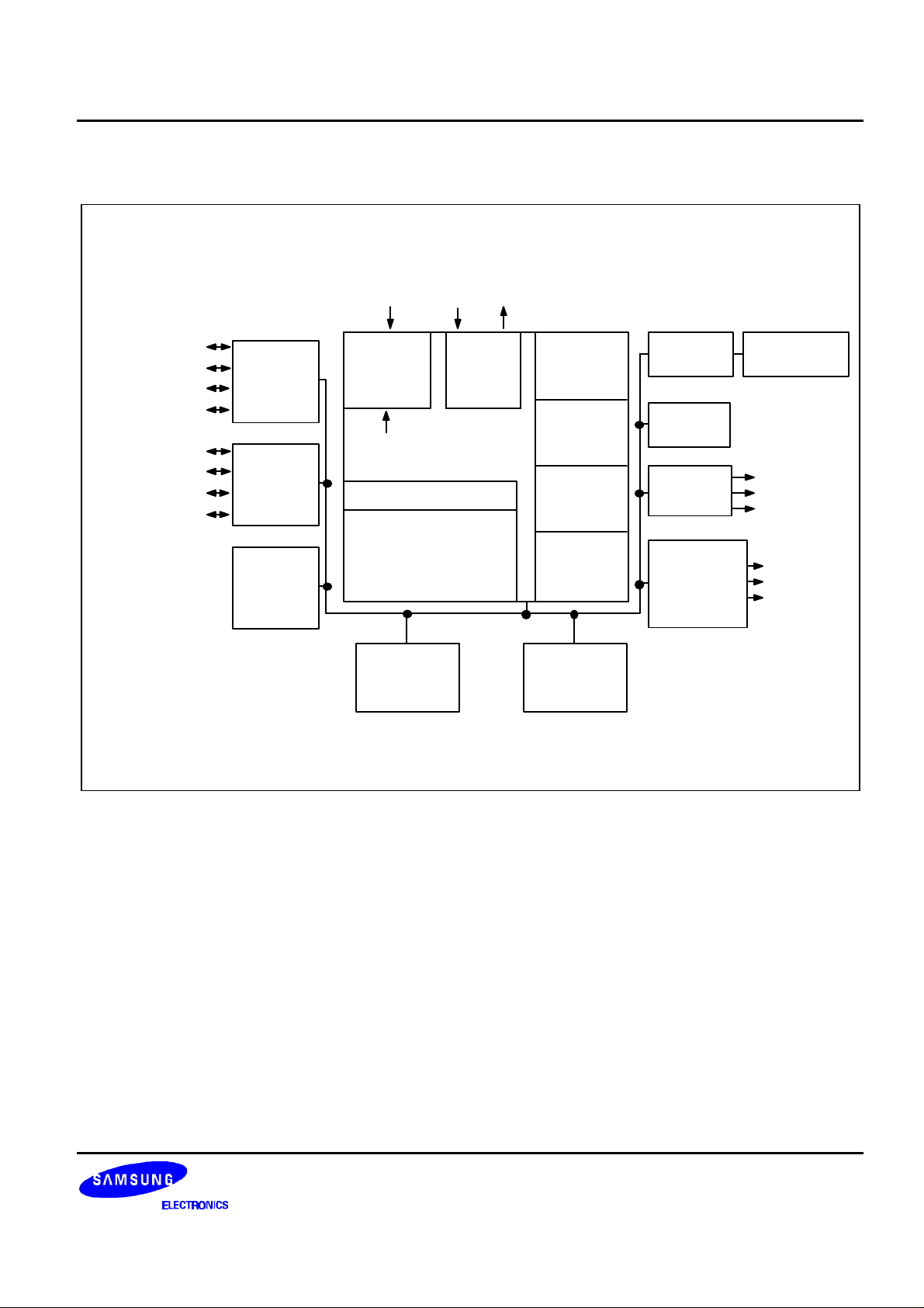
BLOCK DIAGRAM
Xin
RESET
XTin
Xout
XTout
P0.3/BUZ/K3
P0.2/CLO/ /K2
P0.1/ /K1
P0.0/TCLO0/K0
BUZ
TCLO0
P1.3/INT
P1.2/INT2
P1.1/INT1
P1.0/INT0
I/O PORT 0
I/O PORT 1
8-BIT
TIMER/
COUNTER
INTERRUPT
CONTROL
BLOCK
INTERNAL
INTERRUPT
INSTRUCTION DECODER
ARITHMETIC
AND
LOGIC UNIT
256 x 4-BIT
DATA
MEMORY
CLOCK
INSTRUCTION
REGISTER
PROGRAM
COUNTER
PROGRAM
STATUS
WORD
STACK
POINTER
16K BYTES
PROGRAM
MEMORY
BASIC
TIMER
WATCH
TIMER
VOLTAGE
DOUBLER
LCD
DRIVER/
CONTROLLER
WATCH-DOG
TIMER
BIAS
CA
CB
SEG0-SEG43
COM0-COM15
VLC0
Figure 1-1. KS57C2916 Simplified Block Diagram
1-3
PRODUCT OVERVIEW KS57C2916/P2916 MICROCONTROLLER
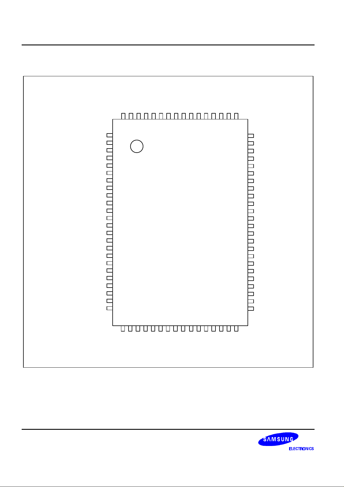
PIN ASSIGNMENTS
SEG40
SEG39
SEG38
SEG37
SEG36
SEG35
SEG34
SEG33
SEG32
SEG31
SEG30
SEG29
SEG28
SEG27
SEG26
SEG25
80
79
78
77
76
75
74
73
72
71
70
69
68
67
66
65
SEG41
SEG42
SEG43
P1.3/INT4
P1.2/INT2
P1.1/INT1
P1.0/INT0
P0.3/BUZ/K3
P0.2/CLO/
P0.1/
P0.0/TCLO0/K0
BUZ
TCLO0
RESET
COM15
/K2
/K1
VDD
VSS
Xout
Xin
TEST
XTin
XTout
CA
CB
VLC0
BIAS
1
2
3
4
5
6
7
8
9
10
11
12
13
14
15
16
17
18
19
20
21
22
23
24
KS57C2916
(TOP VIEW)
64
63
62
61
60
59
58
57
56
55
54
53
52
51
50
49
48
47
46
45
44
43
42
41
SEG24
SEG23
SEG22
SEG21
SEG20
SEG19
SEG18
SEG17
SEG16
SEG15
SEG14
SEG13
SEG12
SEG11
SEG10
SEG9
SEG8
SEG7
SEG6
SEG5
SEG4
SEG3
SEG2
SEG1
1-4
25
26
27
28
29
30
31
32
33
34
35
36
37
38 3940
COM14
COM13
COM12
COM9
COM11
COM10
COM8
COM7
COM6
COM5
COM4
COM3
COM2
COM1
COM0
SEG0
Figure 1-2. KS57C2916 80-QFP Pin Assignment Diagram
KS57C2916/P2916 MICROCONTROLLER PRODUCT OVERVIEW
PIN DESCRIPTIONS
Table 1-1. KS57C2916 Pin Descriptions
Pin Name Pin
Type
P0.0
I/O 4-bit I/O port.
P0.1
P0.2
P0.3
1-bit and 4-bit read/write and test are possible.
Individual pins are software configurable as input or
output.
Individual pins are software configurable as open-
Description Circuit
Type
E-1 11
Number Share Pin
TCLO0/K0
10
9
8
TCLO0/K1
CLO/BUZ/K2
BUZ/K3
drain or push-pull output.
Individual pull-up resistors are software assignable;
pull-up resistors are automatically disabled for
output pins.
P1.0
P1.1
P1.2
P1.3
INT0, INT1 I/O External interrupts. The triggering edge for INT0
I/O Same as port 0. E-1 7
7, 6 P1.0, P1.1
INT0
6
5
4
INT1
INT2
INT4
and INT1 is selectable.
INT2 I/O Quasi-interrupt with detection of rising or falling
5 P1.2
edges
INT4 I/O External interrupt with detection of rising or falling
4 P1.3
edges.
BUZ I/O 2 kHz, 4 kHz, 8 kHz or 16 kHz frequency output for
8 P0.3/K3
buzzer sound.
BUZ
I/O Inverted BUZ signal 9 P0.2/CLO/K2
CLO I/O Clock output 9 P0.2/BUZ/K2
TCLO0
I/O Inverted Timer/counter 0 clock output 10 P0.1/K1
TCLO0 I/O Timer/counter 0 clock output 11 P0.0/K0
COM0–COM15 O LCD common signal output H-6 39–24 –
SEG0–SEG43 O LCD segment signal output H-6 40–80,
1–3
–
1-5
PRODUCT OVERVIEW KS57C2916/P2916 MICROCONTROLLER
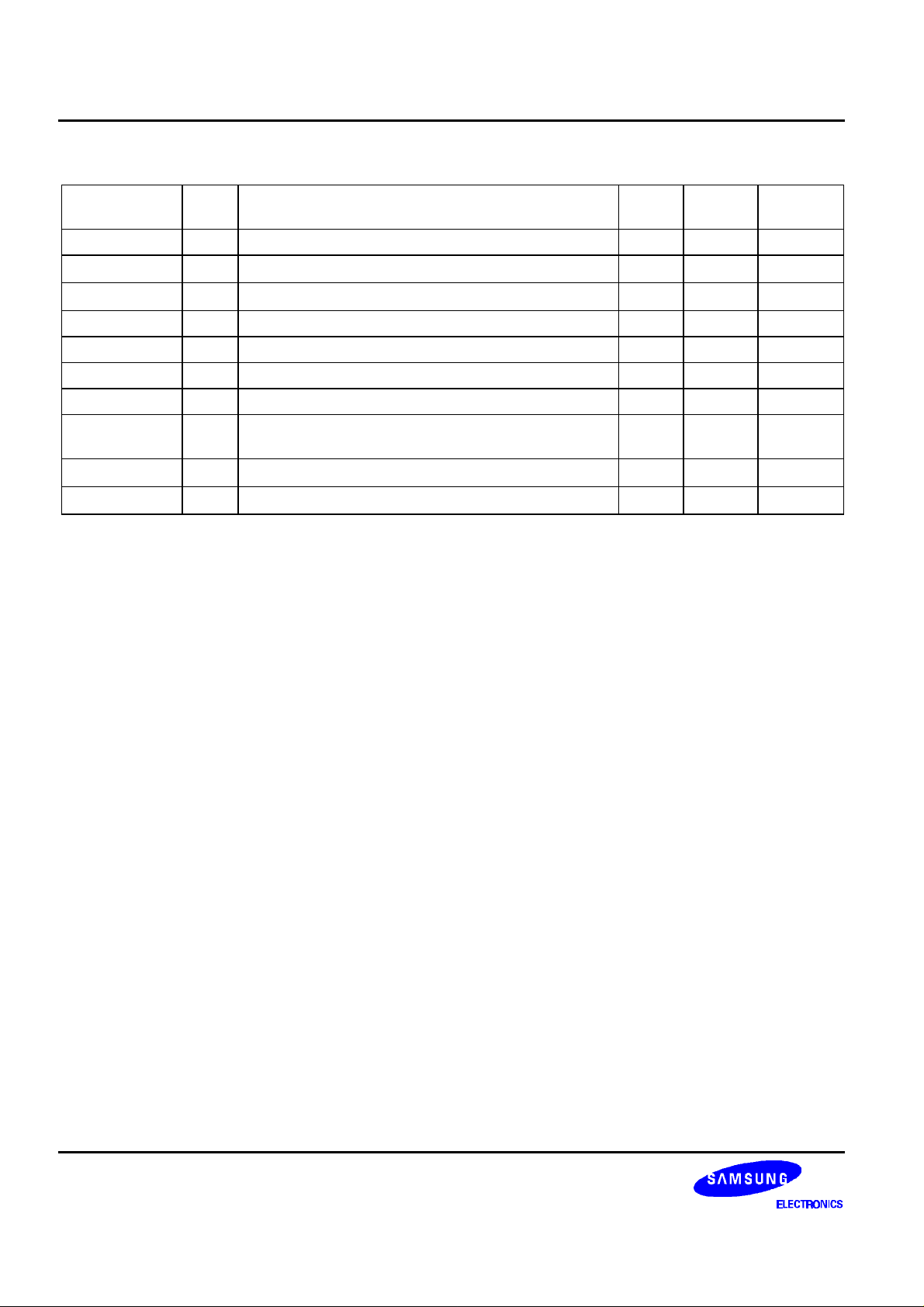
Table 1-1. KS57C2916 Pin Descriptions (Continued)
Pin Name Pin
Type
Description Circuit
Type
Number Share Pin
K0–K3 I/O External interrupt (triggering edge is selectable) E-1 11–8 P0.0–P0.3
V
DD
V
SS
RESET
– Power supply – 12 –
– Ground – 13 –
I Reset input (active low) B 19 –
CA, CB – Capacitor terminal for voltage doubling – 20, 21 –
VCL0 – LCD power supply input – 22 –
BIAS O Doubling voltage level output – 23 –
X
in, Xout
– Crystal, ceramic or RC oscillator pins for system
– 15, 14 –
clock
XT
in, XTout
TEST I
NOTE: Pull-up resistors for all I/O ports are automatically disabled if they are configured to output mode.
– Crystal oscillator pins for subsystem clock – 17, 18 –
Test input (must be connected to VSS)
– 16 –
1-6

KS57C2916/P2916 MICROCONTROLLER PRODUCT OVERVIEW
PIN CIRCUIT DIAGRAMS
V
VDD
PNE
VDD
DD
PULL-UP
RESISTOR
P-CHANNEL
IN
N-CHANNEL
Figure 1-3. Pin Circuit Type A
V
DD
DATA
OUTPUT
DISABLE
V
LC0
V
LC1
P-CH
N-CH
SCHMITT TRIGGER
RESISTOR
ENABLE
Figure 1-5. Pin Circuit Type E-1
I/O
PULL-UP
RESISTOR
IN
SCHMITT TRIGGER
Figure 1-4. Pin Circuit Type B
V
LC2
SEG/COM DATA
V
LC3
V
LC4
V
SS
Figure 1-6. Pin Circuit Type H-6
OUT
1-7

PRODUCT OVERVIEW KS57C2916/P2916 MICROCONTROLLER
NOTES
1-8

KS57C2916/P2916 MICROCONTROLLER ELECTRICAL DATA
13 ELECTRICAL DATA
OVERVIEW
In this section, information on KS57C2916 electrical characteristics is presented as tables and graphics.
The information is arranged in the following order:
Standard Electrical Characteristics
— Absolute maximum ratings
— D.C. electrical characteristics
— Main system clock oscillator characteristics
— Subsystem clock oscillator characteristics
— I/O capacitance
— A.C. electrical characteristics
— Operating voltage range
Miscellaneous Timing Waveforms
— A.C timing measurement point
— Clock timing measurement at X
— Clock timing measurement at XT
— TCL timing
— Input timing for RESET
— Input timing for external interrupts
— Serial data transfer timing
Stop Mode Characteristics and Timing Waveforms
— RAM data retention supply voltage in stop mode
— Stop mode release timing when initiated by RESET
— Stop mode release timing when initiated by an interrupt request
in
in
13-1

ELECTRICAL DATA KS57C2916/P2916 MICROCONTROLLER
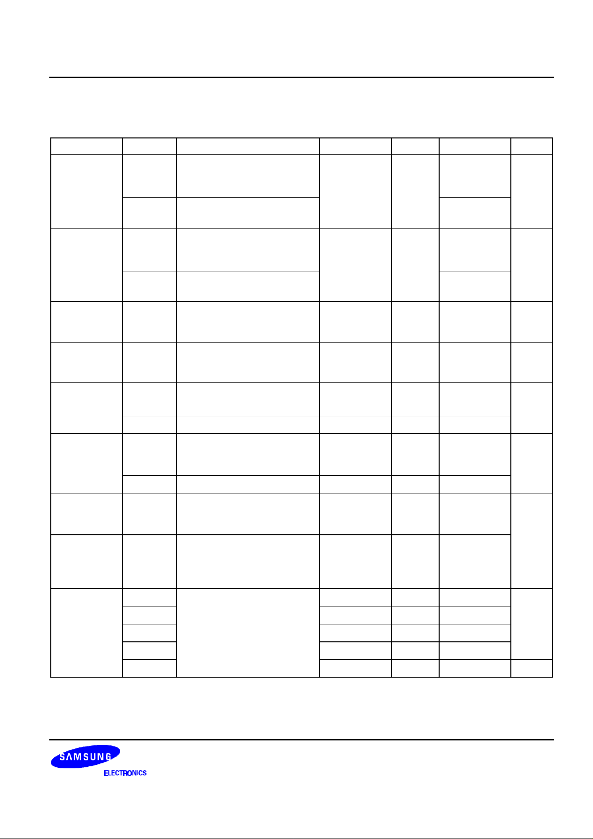
Table 13-1. Absolute Maximum Ratings
(TA = 25 °C)
Parameter Symbol Conditions Rating Units
Supply Voltage
Input Voltage
Output Voltage
Output Current High
V
V
I
DD
V
O
OH
– – 0.3 to + 4.5 V
Ports 0, 1 – 0.3 to VDD + 0.3 V
I
– – 0.3 to VDD + 0.3 V
One I/O pin active – 15 mA
All I/O pins active – 30
Output Current Low
I
OL
One I/O pin active + 30 (Peak value) mA
(note)
+ 15
Total for pins 0, 1 + 100 (Peak value)
(note)
+ 60
Operating Temperature
Storage Temperature
T
A
T
stg
– – 40 to + 85
– – 65 to + 150
°
C
°
C
NOTE: The values for Output Current Low ( IOL ) are calculated as Peak Value × Duty .
Table 13-2. D.C. Electrical Characteristics
(T
= – 40 °C to + 85 °C, VDD = 2.2 V to 3.4 V)
A
Parameter Symbol Conditions Min Typ Max Units
Input High
V
IH1
Ports 0, 1, and RESET
0.8V
DD
–
V
DD
Voltage
Input Low
V
IH2
V
IL1
Xin, X
, and XT
out
in
VDD – 0.1 V
Ports 0, 1, and RESET – –
0.2V
DD
DD
Voltage
Output High
Voltage
V
IL2
V
OH
Xin, X
, and XT
out
in
VDD = 2.2 V to 3.4 V
IOH = – 1 mA
VDD – 1.0
0.1
– – V
Ports 0, 1
Output Low
Voltage
V
OL
V
= 2.2 V to 3.4 V
DD
IOL = 5 mA
– – 1.0 V
Ports 0, 1
V
V
13-2
KS57C2916/P2916 MICROCONTROLLER ELECTRICAL DATA
Table 13-2. D.C. Electrical Characteristics (Continued)
(T
= – 40 °C to + 85 °C, VDD = 2.2 V to 3.4 V)
A
Parameter Symbol Conditions Min Typ Max Units
Input High
Leakage
Current
Input Low
Leakage
Current
Output High
Leakage
I
LIH1
I
LIH2
I
LIL1
I
LIL2
I
LOH
VI = V
DD
All input pins except those
specified below for I
VI = V
DD
Xin, X
V
= 0 V
I
and XT
out
LIH2
in
All input pins except RESET
X
, X
out
= 0 V
and XT
, X
in
DD
in
and XT
out
in
in
V
I
RESET, X
VO = V
All output pins
– – 3 µA
20
– – – 3 µA
– 20
– – 3 µA
Current
Output Low
Leakage
I
LOL
VO = 0 V
All output pins
– – – 3 µA
Current
Pull-Up
Resistor
LCD Voltage
R
R
R
LCD1
L1
L2
V
= 0 V; V
I
DD
Ports 0, 1
V
= 0 V; V
I
DD
Ta = + 25 °C
= 3V
= 3V; RESET
50 100 200
200 450 800
50 100 150
kΩ
kΩ
Dividing
Resistor
V
Voltage Drop
(1)
DD-COMi
R
LCD2
V
DC
Ta = + 25 °C
V
= 3.0 V
LCD
– 15 µA per common pin
25 50 75
– – 120 mV
(i = 0–15)
V
LCD-
SEGx
V
DS
V
LCD
= 3.0 V
– – 120
– 15 µA per common pin
Voltage Drop
(x = 0–43)
Middle Output
Voltage
(2)
V
V
V
V
V
LC0
LC1
LC2
LC3
LC4
V
LC0 =
5.0 V V
-0.2 V
LC0
0.8V
LC0
0.6V
LC0
0.4V
LC0
0.2V
LC0
LC0
-0.2 0.8V
-0.2 0.6V
-0.2 0.4V
-0.2 0.2V
LC0
LC0
LC0
LC0
V
LC0
0.8V
0.6V
0.4V
0.2V
+0.2
LC0
LC0
LC0
LC0
V
+0.2
+0.2
+0.2
+0.2
NOTES:
1. RLCD1 is LCD voltage dividing resistor when LCON.2 = "0", and RLCD2 when LCON.2 = "1".
2. It is middle output voltage when 1/16 duty and 1/5 bias.
13-3
 Loading...