

Samsung KS57P5532, KS57C5532 Datasheet

KS57C5532/P5532 PRODUCT OVERVIEW
1 PRODUCT OVERVIEW
OVERVIEW
The KS57C5532/P5532 single-chip CMOS microcontroller has been designed for high-performance using
Samsung's newest 4-bit CPU core, SAM47 (Samsung Arrangeable Microcontrollers). The KS57P5532 is a
microcontroller which has 32-kbyte one-time-programmable EPROM but its functions are same to KS57C5532.
With its DTMF generator, 8-bit serial I/O interface, and versatile 8-bit timer/counters, the KS57C5532/P5532
offers an excellent design solution for a wide variety of telecommunication applications.
Up to 55 pins of the 64-pin SDIP or QFP package can be dedicated to I/O. Seven vectored interrupts provide fast
response to internal and external events. In addition, the KS57C5532/P5532's advanced CMOS technology
provides for low power consumption and a wide operating voltage range.
DEVELOPMENT SUPPORT
The Samsung Microcontroller Development System, SMDS, provides you with a complete PC-based development environment for KS57-series microcontrollers that is powerful, reliable, and portable. In addition to its
window-based program development structure, the SMDS toolset includes versatile debugging, trace, instruction
timing, and performance measurement applications.
The Samsung Generalized Assembler (SAMA) has been designed specifically for the SMDS environment and
accepts assembly language sources in a variety of microprocessor formats. SAMA generates industry-standard
hex files that also contain program control data for SMDS compatibility.
1-1

PRODUCT OVERVIEW KS57C5532/P5532
FEATURES SUMMARY
Memory
• 1 K × 4-bit RAM
• 32 K × 8-bit ROM
55 I/O Pins
• Input only: 4 pins
• I/O: 43 pins
• N-channel open-drain I/O (S/W): 8 pins
Memory-Mapped I/O Structure
• Data memory bank 15
DTMF Generator
• 16 dual-tone frequencies for tone dialing
8-bit Basic Timer
• Programmable internal timer
• Watchdog timer
Two 8-bit Timer/Counters
• Programmable interval timer
• External event counter function
• Timer/counters clock outputs to TCLO0 and
TCLO1 pins
• External clock signal divider
• Serial I/O interface clock generator
Bit Sequential Carrier
• Supports 8-bit serial data transfer in arbitrary
format
Interrupts
• 3 external interrupt vectors
• 4 internal interrupt vectors
• 2 quasi-interrupts
Power-Down Modes
• Idle: Only CPU clock stops
• Stop: Main system clock stops
• Subsystem clock stop mode
Oscillation Sources
• Crystal, ceramic for main system clock
• Crystal oscillator for subsystem clock
• Main system clock frequency:
3.579545 MHz (typical)
• Subsystem clock frequency: 32.768 kHz (typical)
• CPU clock divider circuit (by 4, 8, or 64)
Instruction Execution Times
• 0.67, 1.33, 10.7 µs at 6.0 MHz
• 1.12, 2.23, 17.88 µs at 3.579545 MHz
• 122 µs at 32.768 kHz
Watch Timer
• Time interval generation:
0.5 s, 3.9 ms at 32.768 kHz
• 4 frequency outputs to the BUZ pin
8-bit Serial I/O Interface
• 8-bit transmit/receive mode
• 8-bit receive mode
• LSB-first or MSB-first transmission selectable
1-2
Operating Temperature
• – 40 °C to 85 °C
Operating Voltage Range
• 1.8 V to 5.5 V (at 3 MHz)
• 2.7 V to 5.5 V (at 6 MHz)
Package Types
• 64 SDIP, 64 QFP
KS57C5532/P5532 PRODUCT OVERVIEW
P13.0-P13.2
P12.0-P12.3
P11.0-P11.3
P10.0-P10.3
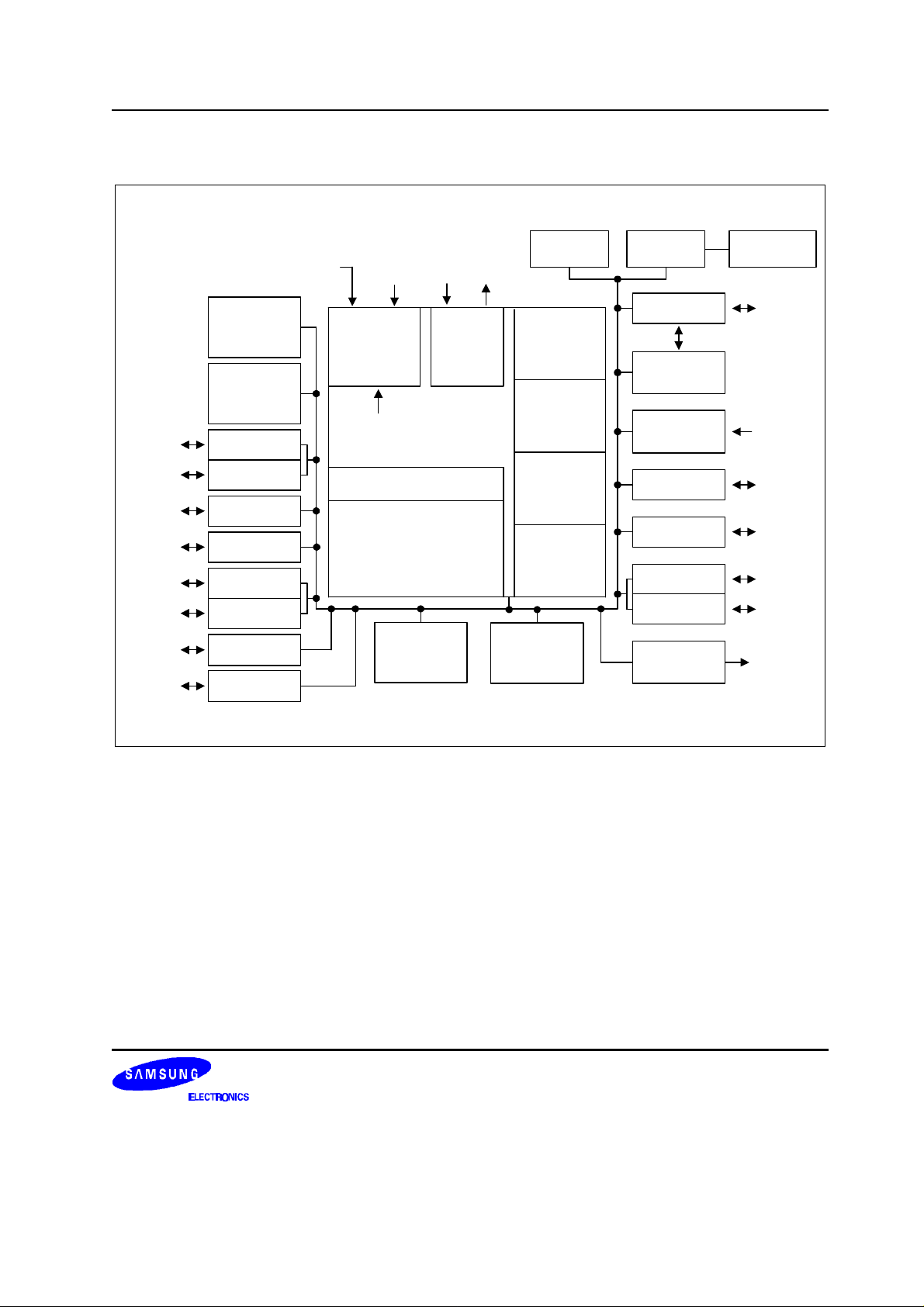
BLOCK DIAGRAM
P6.0-P6.3/
KS0-KS3
P7.0-P7.3/
KS4-KS7
P8.0-P8.3
P9.0-P9.3
INT0, INT1, INT2 INT4
8-BIT
Timer/
Counter 0
8-BIT
Timer/
Counter 1
I/O Port 6
I/O Port 7
I/O Port 8
I/O Port 9
I/O Port 10
I/O Port 11
I/O Port 12
I/O Port 13
RESET
Interrupt
Control
Block
Internal
Interrupts
Instruction Decoder
Arithmetic
and
Logic Unit
1 K x 4-BIT
Data
Memory
XT
X
IN
IN
Clock
XT
X
OUT
OUT
Watch
Timer
Stack
Pointer
Basic
Timer
I/O Port 0
Serial I/O
Watch-Dog
Timer
P0.0/
SCK
P0.1/SO
P0.2/SI
P0.3/BTCO
Port
Program
Counter
Program
Status
Word
Flags
Input
Port1
I/O Port 2
I/O Port 3
I/O Port 4
I/O Port 5
P1.0/INT0
P1.1/INT1
P1.2/INT2
P1.3/INT4
P2.0/TCLO0
P2.1/TCLO1
P2.2/CLO
P2.3/BUZ
P3.0/TCLO0
P3.1/TCLO1
P3.2
P3.3
P4.0-P4.3
P5.0-P5.3
32 K Byte
Program
Memory
DTMF
Generator
DTMF
Figure 1-1. KS57C5532/P5532 Simplified Block Diagram
1-3

PRODUCT OVERVIEW KS57C5532/P5532
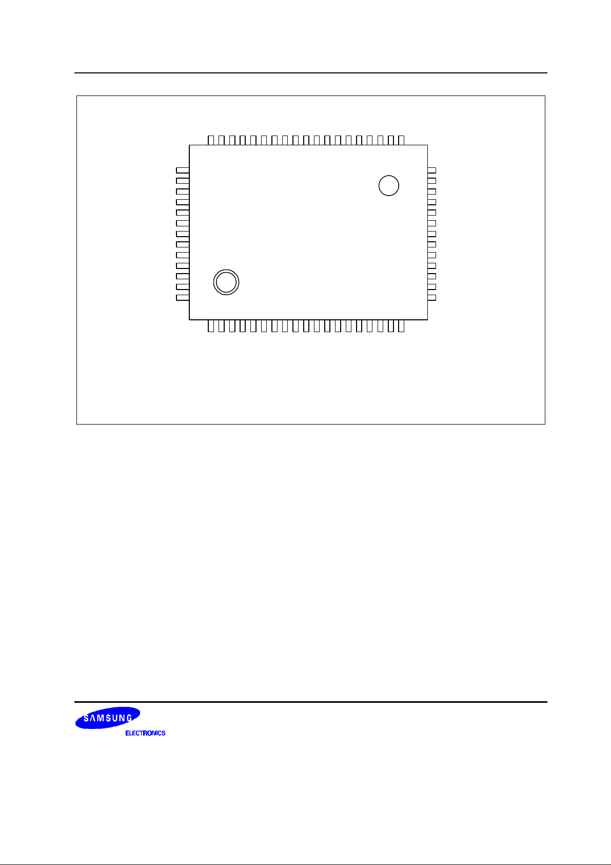
PIN ASSIGNMENTS
VSS
P1.3/INT4
P1.2/INT2
P1.1/INT1
P1.0/INT0
P13.2
P13.1
P13.0
P2.3/BUZ
P2.2/CLO
P2.1/TCLO1
P2.0/TCLO0
P0.3/BTCO
P0.2/SI
P0.1/SO
P0.0/
SCK
P10.3
P10.2
P10.1
P10.0
P11.3
P11.2
P11.1
P11.0
P12.3
P12.2
P12.1
P12.0
P3.3
P3.2
TEST
DTMF
VDD
1
2
3
4
5
6
7
8
9
10
11
12
13
14
15
16
17
18
19
20
21
22
23
24
25
26
27
28
29
30
31
32
(64-SDIP-750)
KS57C5532
64
63
62
61
60
59
58
57
56
55
54
53
52
51
50
49
48
47
46
45
44
43
42
41
40
39
38
37
36
35
34
33
P9.0
P9.1
P9.2
P9.3
P8.0
P8.1
P8.2
P8.3
P7.0/KS4
P7.1/KS5
P7.2/KS6
P7.3/KS7
P6.0/KS0
P6.1/KS1
P6.2/KS2
P6.3/KS3
XTOUT
XT
IN
X
IN
XOUT
RESET
P5.0
P5.1
P5.2
P5.3
P4.0
P4.1
P4.2
P4.3
P3.0/TCL0
P3.1/TCL1
1-4
Figure 1-2. KS57C5532/P5532 Pin Assignment Diagrams
KS57C5532/P5532 PRODUCT OVERVIEW
51504948474645444342414039383736353433
P8.0
P9.3
P9.2
P9.1
P9.0
SS
V
P1.3/INT4
P1.2/INT2
P1.1/INT1
P1.0/INT0
P13.2
P13.1
P13.0
52
53
54
55
56
57
58
59
60
61
62
63
64
12345678910111213141516171819
P2.3/BUZ
P2.2/CLO
P2.1/TCLO1
KS57C5532
(64-QFP-1420F)
P10.3
P0.2/SI
P0.1/SO
P0.3/BTCO
P2.0/TCLO0
P10.2
P0.0/SCK
P10.1
P10.0
P11.3
P11.2
P11.1
P11.0
P12.3
P12.2
32
31
30
29
28
27
26
25
24
23
22
21
20
P12.1
P5.3
P4.0
P4.1
P4.2
P4.3
P3.0/TCL0
P3.1/TCL1
VDD
DTMF
TEST
P3.2
P3.3
P12.0
Figure 1-2. KS57C5532/P5532 Pin Assignment Diagrams (Continued)
1-5
PRODUCT OVERVIEW KS57C5532/P5532
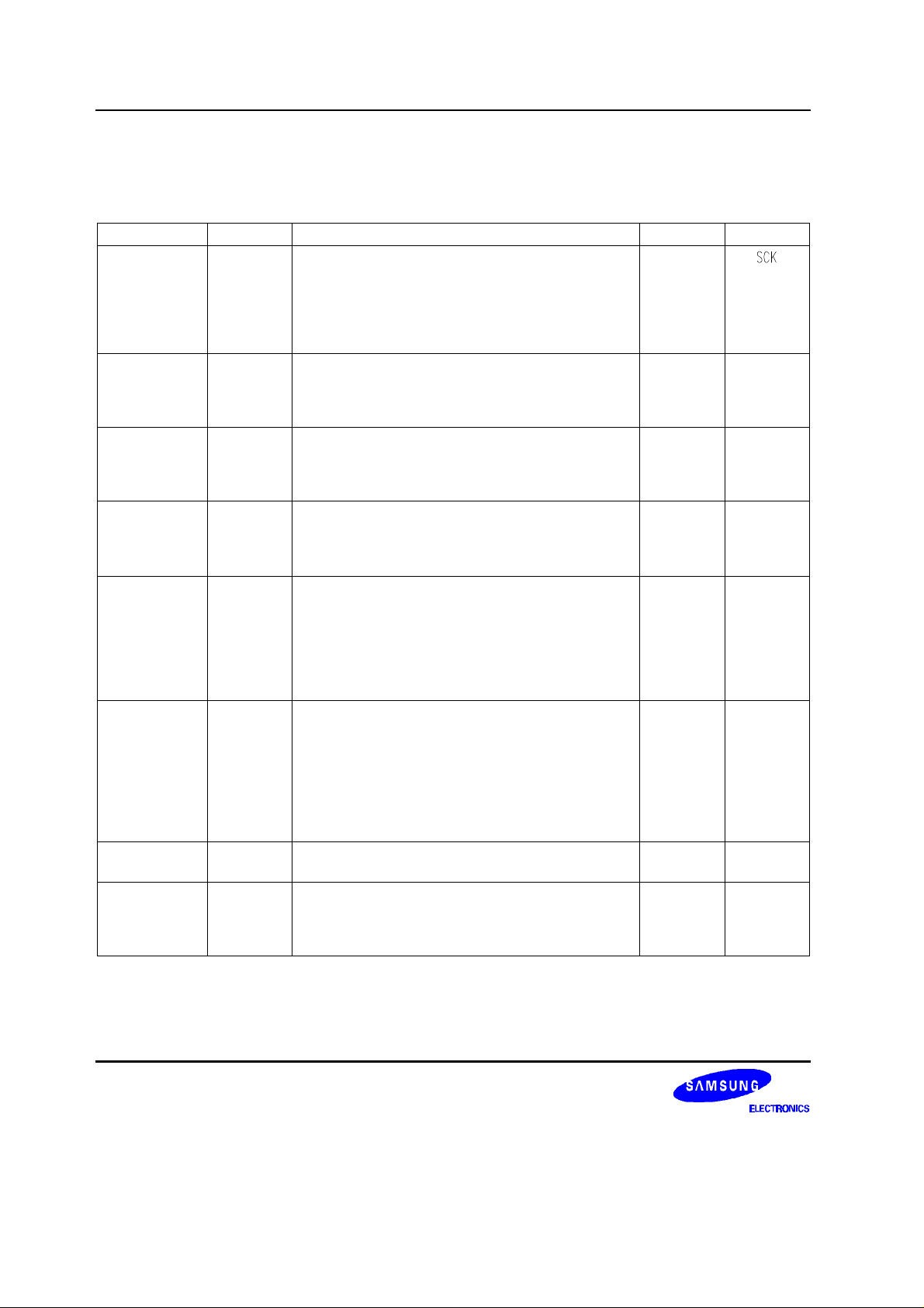
PIN DESCRIPTIONS
Table 1-1. KS57C5532/P5532 Pin Descriptions
Pin Name Pin Type Description Number Share Pin
P0.0
P0.1
P0.2
P0.3
P1.0
P1.1
P1.2
P1.3
P2.0
P2.1
P2.2
P2.3
P3.0
P3.1
P3.2
P3.3
P4.0–P4.3
P5.0–P5.3
P6.0–P6.3
P7.0–P7.3
P8.0–P8.3 I/O Same as port 0. 59–56
P9.0–P9.3 I/O
I/O
4-bit I/O port.
1-bit or 4-bit read/write and test is possible.
Individual pins are software configurable as input or
output.
4-bit pull-up resistors are software assignable; pull-up
resistors are automatically disabled for output pins.
I
4-bit input port.
1-bit and 4-bit read and test is possible.
4-bit pull-up resistors are assignable by software to
port 1.
I/O Same as port 0.
I/O Same as port 0.
I/O
4-bit I/O ports.
1-bit and 4-bit read/write and test is possible.
4-bit pull-up resistors are software assignable to input
pins and are automatically disable for output pins.
N-channel open-drain or push-pull output can be
selected by software. Port 4 and 5 can be paired to
support 8-bit data transfer.
I/O 4-bit I/O ports.
1-bit or 4-bit read/write and test is possible.
Port 6 pins are individually software configurable as
input or output.
4-bit pull-up resistors are software assignable; pull-up
resistors are automatically disabled for output pins.
Ports 6 and 7 can be paired to enable 8-bit data
transfer.
4-bit I/O port.
1-bit or 4-bit read/write and test is possible.
4-bit pull-up resistors are software assignable; pull-up
resistors are automatically disabled for output pins.
15 (8)
14 (7)
13 (6)
12 (5)
1 (61)
2 (60)
3 (59)
4 (58)
11 (4)
10 (3)
9 (2)
8 (1)
34 (27)
33 (26)
29 (22)
28 (21)
38–35
(31–28)
42–39
(35–32)
51–48
(44–41)
55–52
(48–45)
(52–49)
63–60
(56–53)
SO
SI
BTCO
INT0
INT1
INT2
INT4
TCLO0
TCLO1
CLO
BUZ
TCL0
TCL1
(1)
SCLK
(1)
SDAT
–
KS0–KS3
KS4–KS7
–
–
NOTES
1. SCLK and SDAT are used for KS57P5532 only.
2. Parentheses indicate pin number for 64 QFP package.
1-6
KS57C5532/P5532 PRODUCT OVERVIEW
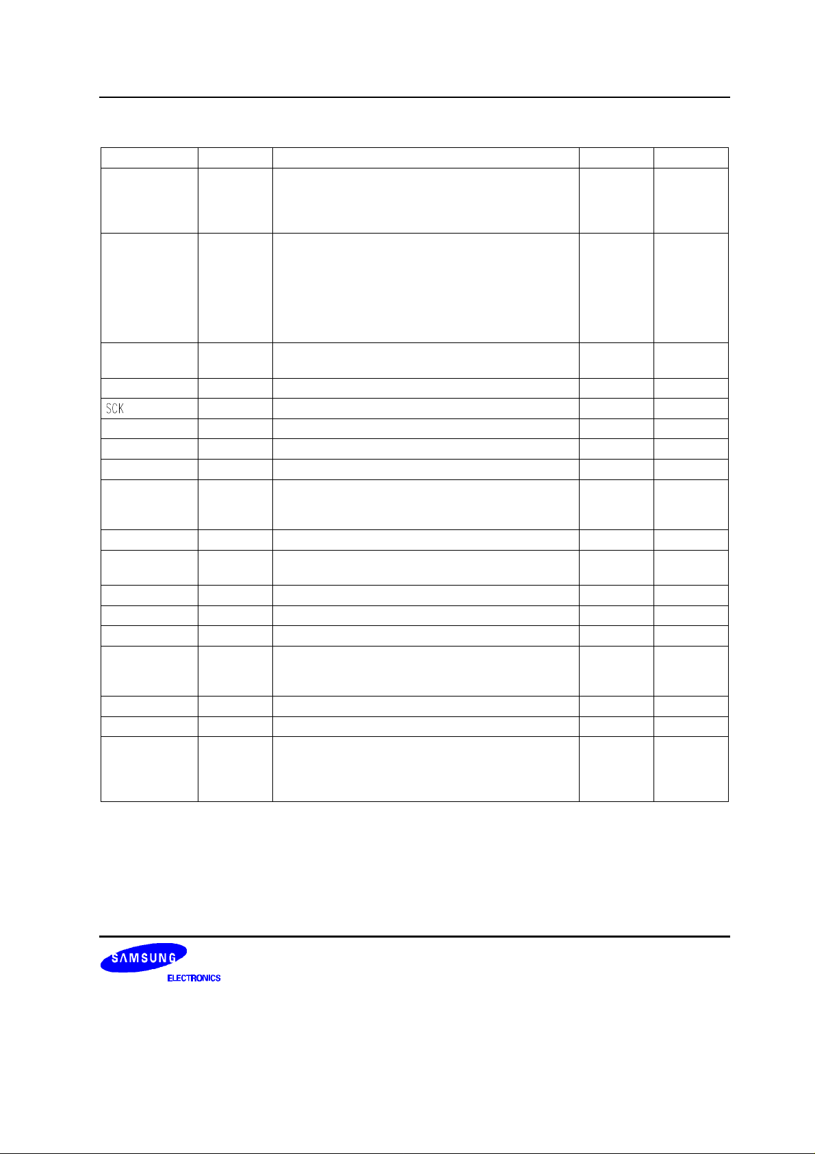
Table 1-1. KS57C5532/P5532 Pin Descriptions (Continued)
Pin Name Pin Type Description Number Share Pin
P10.0–P10.3
P11.0–P11.3
I/O
Same as port 9.
Ports 10 and 11 can be paired to support 8-bit data
transfer.
19–16
(12–9)
23–20
–
(16–13)
P12.0–P12.3 I/O
4-bit I/O port.
1-bit or 4-bit read/write and test is possible.
27–24
(20–17)
–
Individual pins are software configurable as input or
output.
4-bit pull-down resistors are software assignable;
pull-down resistors are automatically disabled for
output pins.
P13.0–P13.2 I/O 3-bit I/O port; characteristics are same as port 9. 7–5
–
(64–62)
DTMF O DTMF output. 31 (24) –
I/O Serial I/O interface clock signal 15 (8) P0.0
SO I/O Serial data output 14 (7) P0.1
SI I/O Serial data input 13 (6) P0.2
BTCO I/O Basic timer clock output 12 (5) P0.3
INT0, INT1 I
External interrupts. The triggering edge for INT0 and
INT1 is selectable. INT0 is synchronized to system
4, 3
(61, 60)
P1.0, P1.1
clock.
INT2 I Quasi-interrupt with detection of rising edges 2 (59) P1.2
INT4 I
External interrupt with detection of rising and falling
1 (58) P1.3
edges.
TCLO0 I/O Timer/counter 0 clock output 11 (4) P2.0
TCLO1 I/O Timer/counter 1 clock output 10 (3) P2.1
CLO I/O Clock output 9 (2) P2.2
BUZ I/O
2 kHz, 4 kHz, 8 kHz, or 16 kHz frequency output at
8 (1) P2.3
the watch timer clock frequency of 32.768 kHz for
buzzer sound
TCL0 I/O External clock input for timer/counter 0 34 (27) P3.0
TCL1 I/O External clock input for timer/counter 1 33 (26) P3.1
KS0–KS3
I/O Quasi-interrupt inputs with falling edge detection
51–48
P6.0–P6.3
(44–41)
KS4–KS7
55–52
P7.0–P7.3
(48–45)
NOTE: Parentheses indicate pin number for 64 QFP package.
1-7
PRODUCT OVERVIEW KS57C5532/P5532
Table 1-1. KS57C5532/P5532Pin Descriptions (Concluded)
Pin Name Pin Type Description Number Share Pin
V
DD
V
SS
– Power supply 32 (25) –
– Ground 64 (57) –
I Reset signal 43 (36) –
X
IN, XOUT
XT
XT
IN,
OUT
TEST – Chip test input pin.
–
Crystal, ceramic, or R/C oscillator signal for main
system clock. (For external clock input, use XIN and
input XIN's reverse phase to X
OUT
)
– Crystal oscillator signal for subsystem clock.
(For external clock input, use XTIN and input XTIN's
reverse phase to XT
OUT
)
45, 44
(38, 37)
46, 47
(39, 40)
30 (23) –
–
–
Hold GND when the device is operating.
NOTE: Parentheses indicate pin number for 64 QFP package.
1-8
KS57C5532/P5532 PRODUCT OVERVIEW
Table 1-2. Overview of KS57C5532/P5532 Pin Data
Pin Names Share Pins I/O Type Reset Value Circuit Type
P0.0–P0.3 , SO, SI, BTCO I/O Input D-4
P1.0–P1.3 INT0, INT1, INT2,
I Input A-1
INT4
P2.0–P2.3 TCLO0, TCLO1, CLO,
I/O Input D-2
BUZ
P3.0–P3.1 TCL0, TCL1 I/O Input D-4
P3.2–P3.3 – I/O Input D-2
P4.0–P4.3
– I/O Input E-2
P5.0–P5.3
P6.0–P6.3
P7.0–P7.3
KS0–KS3
KS4–KS7
I/O
P8.0–P8.3 – I/O
P9.0–P9.3 – I/O
P10.0–P10.3
– I/O
Input
Input
Input
Input
D-4
D-2
D-2
D-2
P11.0–P11.3
P12.0–P12.3 – I/O
P13.0–P13.2 – I/O
DTMF – O
XIN, X
OUT
XTIN, XT
OUT
– – – –
–
Input
Input
High impedence
I – B
D-6
D-2
G-6
NC – – – –
VDD, V
SS
– – – –
1-9

PRODUCT OVERVIEW KS57C5532/P5532
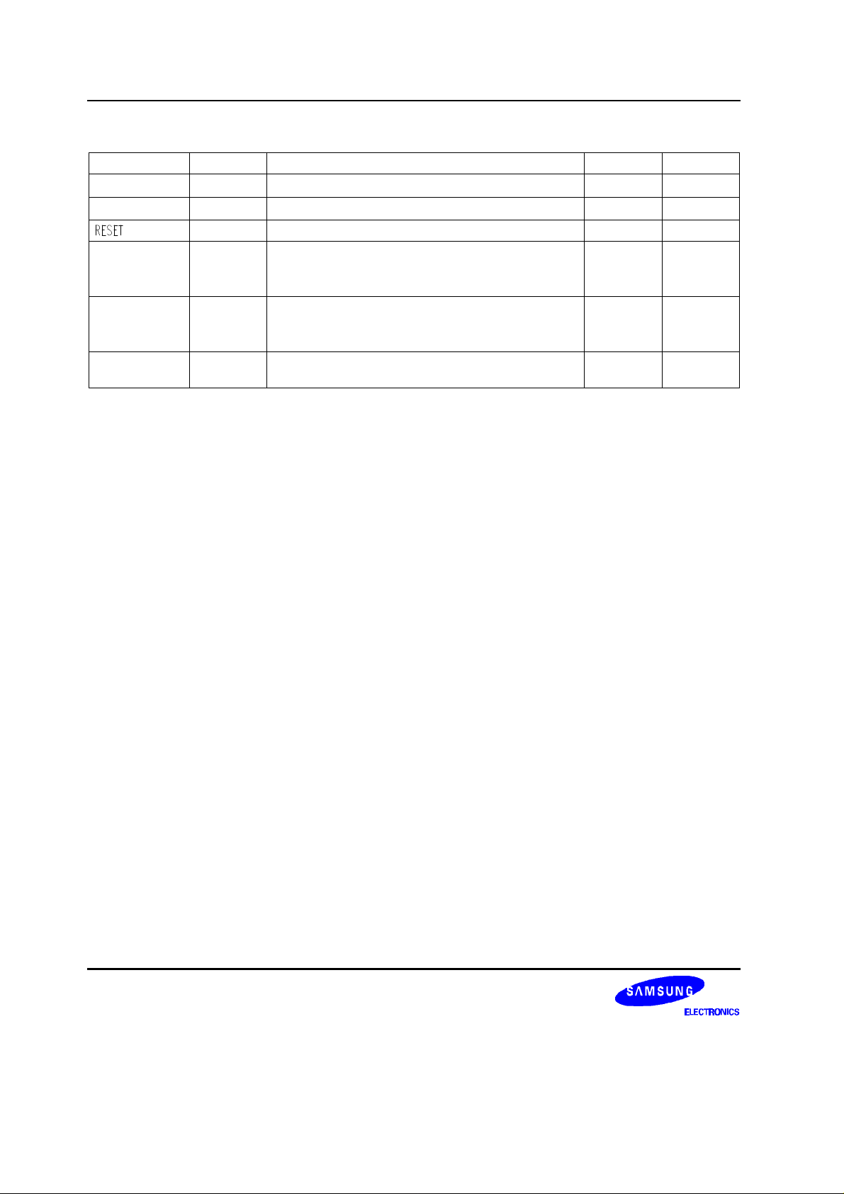
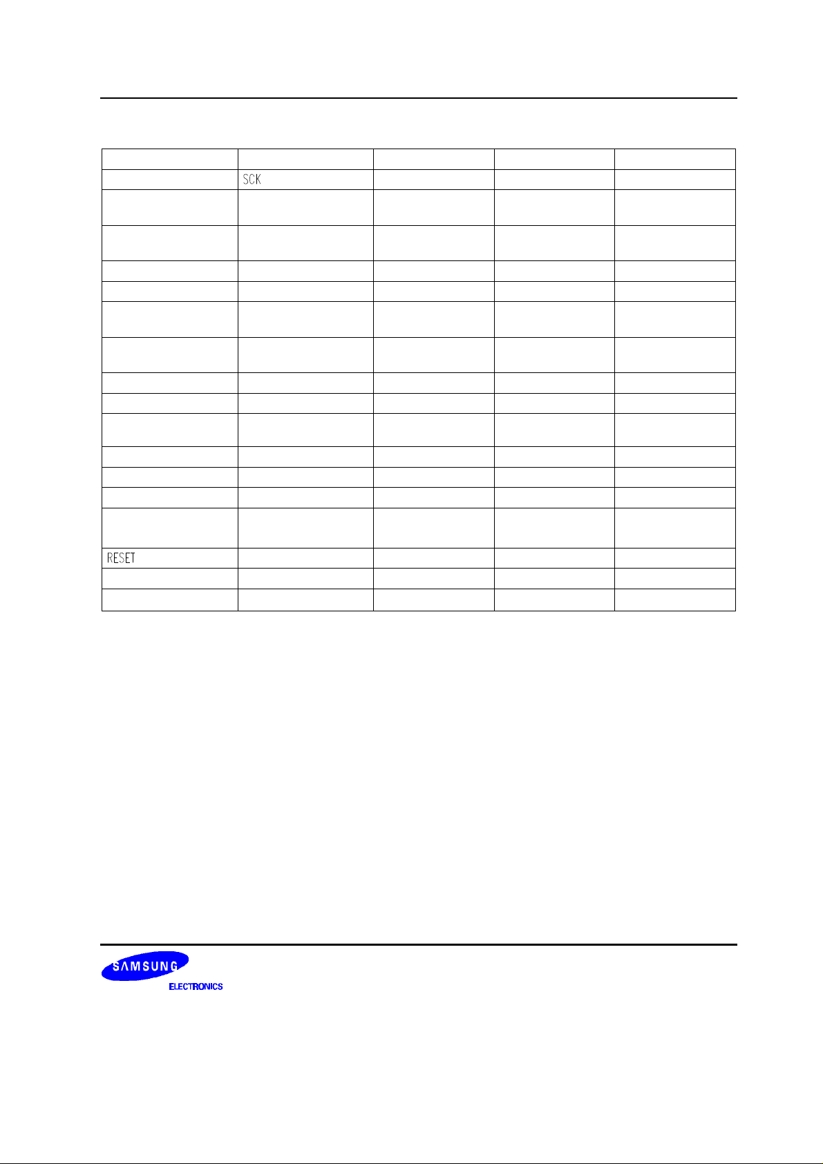
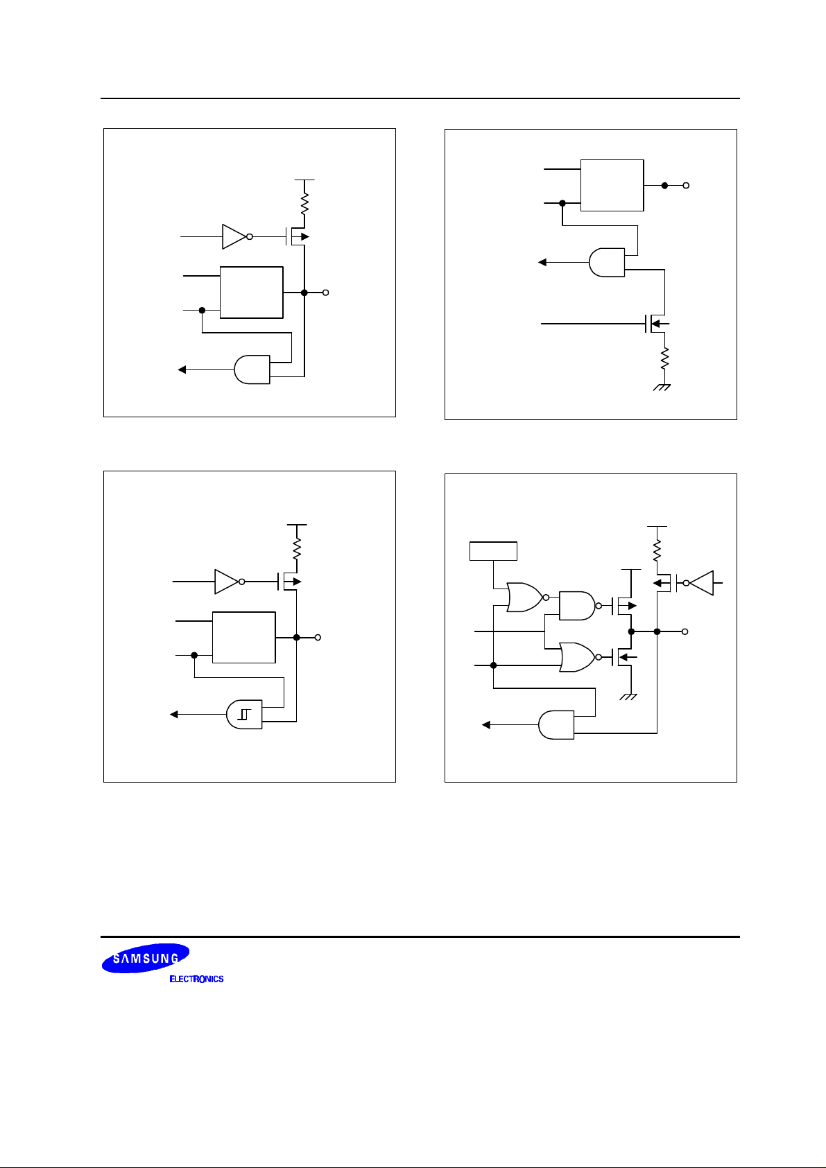
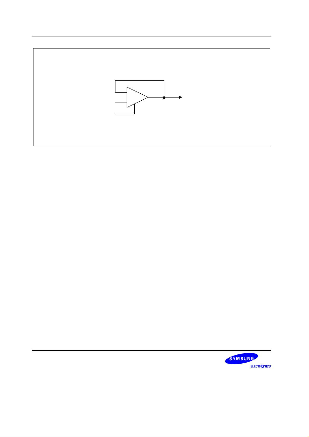
PIN CIRCUIT DIAGRAMS
VDD
P-Channel
In
N-Channel
Figure 1-3. Pin Circuit Type A
VDD
Pull-Up
Resistor
P-Channel
In
Pull-Up
Resistor
Enable
Data
Output
DIsable
VDD
Pull-Up
Resistor
In
Schmitt Trigger
Figure 1-5. Pin Circuit Type B
VDD
P-Channel
Out
N-Channel
1-10
Schmitt Trigger
Figure 1-4. Pin Circuit Type A-1
Figure 1-6. Pin Circuit Type C
KS57C5532/P5532 PRODUCT OVERVIEW
Pull-up
Enable
Data
Output
DIsable
Circuit
Type C
Figure 1-7. Pin Circuit Type D-2
VDD
Pull-up
Enable
Data
Output
Disable
Circuit
Type C
VDD
P-Channel
P-Channel
I/O
I/O
Data
Output
Disable
Data
Output
DIsable
Pull-down
Enable
Circuit
Type C
Figure 1-9. Pin Circuit Type D-6
PNE
VDD
I/O
VDD
Pull-up
Enable
I/O
Schmitt Trigger
Figure 1-8. Pin Circuit Type D-4
Figure 1-10. Pin Circuit Type E-2
1-11
PRODUCT OVERVIEW KS57C5532/P5532
Disable
DTMF Out
+
1-12
 Loading...