

Samsung KS57P5404, KS57C5404 Datasheet

KS57C5404/P5404 PRODUCT OVERVIEW
1 PRODUCT OVERVIEW
OVERVIEW
The KS57C5404 single-chip CMOS microcontroller is designed for high-performance using Samsung’s newest
4-bit CPU core, SAM47 (Samsung Arrangeable Microcontrollers).
With a versatile 8-bit timer/counter and a D/A converter, the KS57C5404 offers an excellent design solution for a
wide variety of telecommunication applications.
Up to 17 pins of the 24-pin SDIP package can be dedicated to I/O. Four vectored interrupts provide fast response
to internal and external events. In addition, the KS57C5404’s advanced CMOS technology has realized
substantially lower power consumption with a wide operating voltage range — all at a substantially lower cost.
OTP
The KS57C5404 microcontroller is also available in OTP (One Time Programmable) version, KS57P5404.
KS57P5404 microcontroller has an on-chip 4-Kbyte one-time-programmable EPROM instead of masked ROM.
The KS57P5404 is comparable to KS57C5404, both in function and in pin configuration.
1-1

PRODUCT OVERVIEW KS57C5404/P5404
FEATURES SUMMARY
Memory
• 512 × 4-bit RAM
• 4096 × 8-bit ROM
I/O Pins
• 17 pins I/O
• N-channel open-drain I/O: 8 pins
8-Bit Basic Timer
• Programmable interval timer
• Watchdog timer
Interval 8-Bit Timer/Counter
• Programmable interval timer
• External event counter function
• Timer/counter clock output to TCLO0 pin
Buzzer Output
• Four frequency output to BUZ pin
D/A Converter
• 8-bit D/A converter
Interrupts
• Two external interrupt vectors
• Two internal interrupt vectors
• One quasi-interrupt
Bit Sequential Carrier
• Supports 16-bit serial data transfer in arbitrary
format
Power-Down Modes
• Idle mode (only CPU clock stops)
• Stop mode (system clock stops)
Oscillation Sources
• Crystal, or ceramic for system clock
• Crystal, ceramic: 0.4–6.0 MHz
• CPU clock divider circuit (by 4, 8, or 64)
Instruction Execution Times
• 0.95, 1.91, and 15.3 µs at 4.19 MHz
• 0.67, 1.33, 10.7 µs at 6.0 MHz
Operating Temperature
• – 40 °C to 85 °C
Operating Voltage Range
• 1.8 V to 5.5 V (at 3 MHz)
• 2.7 V to 5.5 V (at 6 MHz)
Package Types
• 24-pin SOP-375
• 24-pin SDIP-300
Memory-Mapped I/O Structure
• Data memory bank 15
1-2
KS57C5404/P5404 PRODUCT OVERVIEW
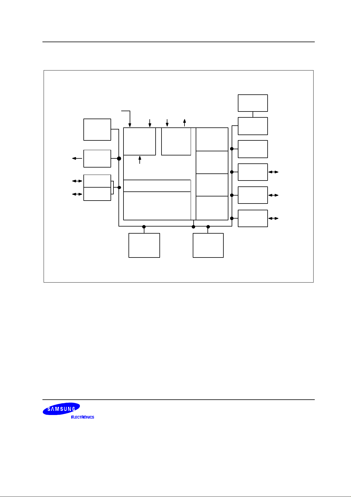
BLOCK DIAGRAM
Watchdog
Timer
Basic
Timer
Buzzer
I/O Port 0
I/O Port 1
P0.0/INT0
P0.1/INT1
P0.2/KS0
P0.3/KS1
P1.0/TCL0
P1.1/TCLO0
P1.2/CLO
P1.3/BUZ
DAO
P4.0–P4.3
P5.0–P5.3
INT0, INT1
8-bit
Timer/
Counter
D/A
Converter
I/O Port 4
I/O Port 5
RESET
Interrupt
Control
Block
Internal
Interrupts
Instruction Decoder
Arithmetic Logic Unit
X
IN
Clock
X
OUT
Stack
Pointer
Program
Counter
Program
Status
Word
Flags
512 x 4-bit
Data
Memory
4 K byte
Program
Memory
Figure 1-1. KS57C5404 Simplified Block Diagram
I/O Port 2
P2.0
1-3

PRODUCT OVERVIEW KS57C5404/P5404
PIN ASSIGNMENTS
VSS
X
OUT
XIN
TEST
P0.0/INT0
DAO
P0.1/INT1
RESET
P0.2/KS0
P0.3/KS1
P1.0/TCL0
P1.1/TCLO0
1
2
3
4
5
6
7
8
9
10
11
12
24 SDIP-300
24 SOP-375
24
23
22
KS57C5404
21
20
19
18
17
16
15
14
13
Figure 1-2. KS57C5404 Pin Assignment Diagrams
VDD
P5.3
P5.2
P5.1
P5.0
P4.3
P4.2
P4.1
P4.0
P2.0
P1.3/BUZ
P1.2/CLO
1-4

KS57C5404/P5404 PRODUCT OVERVIEW
PIN DESCRIPTIONS
Table 1-1. KS57C5404 Pin Descriptions
Pin Name Pin Type Description Share Pin
P0.0
P0.1
P0.2
P0.3
P1.0
P1.1
P1.2
P1.3
P2.0 I/O 1-bit I/O port. 1- or 4-bit read/write and test is possible.
P4.0–P4.3
P5.0–P5.3
INT0 I/O External interrupts with rising/falling edge detection P0.0
INT1 I/O External interrupts with rising/falling edge detection P0.1
KS0
KS1
TCL0 I/O External clock input for timer/counter P1.0
TCLO0 I/O Timer/counter clock output P1.1
CLO I/O CPU clock output P1.2
BUZ I/O 0.5, 1, 2, or 4 kHz frequency output at 4.19 MHz for buzzer sound P1.3
DAO O 8-bit D/A converter output –
VDD – Main power supply –
VSS – Ground –
RESET I Reset signal –
TEST I Chip test input pin. Hold GND when the device is operating. –
XIN, X
OUT
I 4-bit I/O port. 1- or 4-bit read/write and test is possible.
Pull-up resistors are assignable to input pins by software and are
automatically disabled for output pins. Pins are individually configurable
as input or output.
I/O 4-bit I/O port. 1- or 4-bit read/write and test is possible.
Pull-up resistors are assignable to input pins by software and are
TCLO0
automatically disabled for output pins. Pins are individually configurable
as input or output.
Pull-up resistors are assignable to input pins by software and are
automatically disabled for output pins.
I/O
4-bit I/O port. 1- or 4-bit read/write and test is possible.
Pins are individually configurable as input or output.
Pull-up resistors are assignable to input pins by software and are
automatically disabled for output pins.
The N-channel open drain or push-pull output can be selected by
software (1-bit unit).
I/O Quasi-interrupt input with falling edge detection
– Crystal, ceramic oscillator signal for system clock –
INT0
INT1
KS0
KS1
TCL0
CLO
BUZ
–
–
P0.2
P0.3
1-5

PRODUCT OVERVIEW KS57C5404/P5404
Table 1-2. Overview of KS57C5404 Pin Data
SDIP Pin Numbers Share Pins I/O Type Reset Value Circuit Type
V
X
SS
OUT
, X
IN
– – – –
– – – –
TEST – I – –
P0.0, P0.1 INT0, INT1 I/O Input D-4
RESET – I – B
P0.2
P0.3
P1.0
P1.1
P1.2
P1.3
KS0
KS1
TCL0
TCLO0
CLO
BUZ
I/O Input D-4
I/O Input D-2
P2.0 – I/O Input D-2
DAO – O Output –
P4.0–P4.3 – I/O Input E-2
P5.0–P5.3 – I/O Input E-2
V
DD
– – – –
1-6
KS57C5404/P5404 PRODUCT OVERVIEW
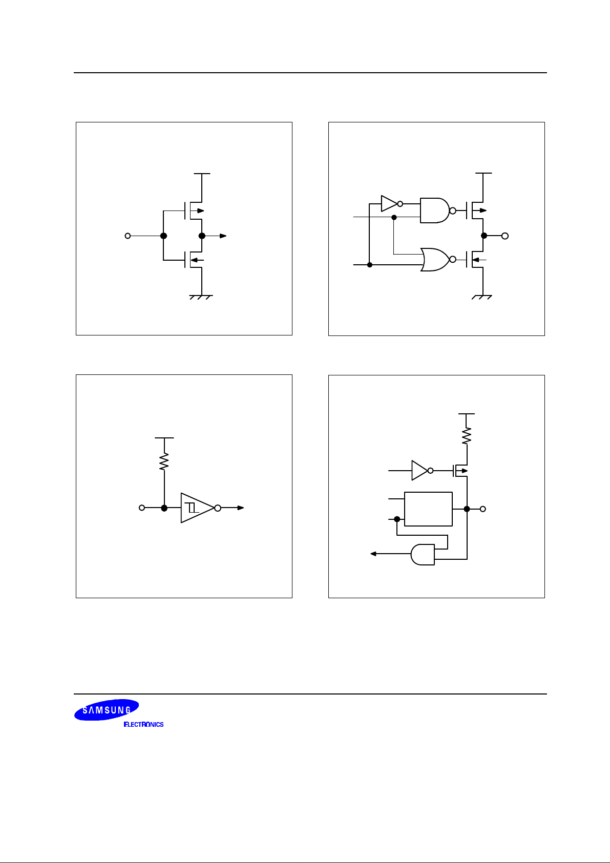
PIN CIRCUIT DIAGRAMS
V
DD
P-Channel
IN
N-Channel
Figure 1-3. Pin Circuit Type A
V
DD
Pull-up
Resistor
Data
Output
Disable
Figure 1-5. Pin Circuit Type C
V
DD
Pull-up
Enable
V
DD
P-Channel
N-Channel
P-Channel
Out
IN
Schmitt Trigger
Figure 1-4. Pin Circuit Type B
Data
Output
Disable
Circuit
Type C
Figure 1-6. Pin Circuit Type D-2
In/Out
1-7
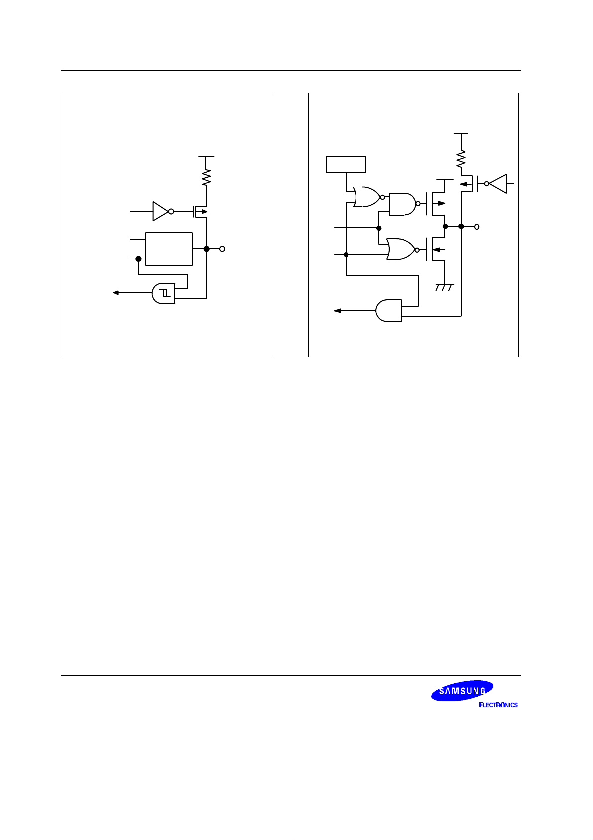
PRODUCT OVERVIEW KS57C5404/P5404 (Preliminary Spec)
V
DD
V
DD
PNE
V
DD
Pull-Up
Resistor
Pull-up
Enable
Data
Output
Circuit
Type C
P-Channel
Disable
Figure 1-7. Pin Circuit Type D-4
Resistor
Enable
In/Out
Data
In/Out
Output
Disable
Figure 1-8. Pin Circuit Type E-2
1-8

KS57C5404/P5404 ELECTRICAL DATA
14 ELECTRICAL DATA
OVERVIEW
In this section, KS57C5404 electrical characteristics are presented in tables and graphs. The information is
arranged in the following order:
Standard Electrical Characteristics
— Absolute maximum ratings
— D.C. electrical characteristics
— Main system clock oscillator characteristics
— Subsystem clock oscillator characteristics
— I/O capacitance
— A.C. electrical characteristics
— Operating voltage range
Miscellaneous Timing Waveforms
— A.C timing measurement point
— Clock timing measurement at X
— Clock timing measurement at XT
— TCL timing
— Input timing for RESET
— Input timing for external interrupts
— Serial data transfer timing
Stop Mode Characteristics and Timing Waveforms
— RAM data retention supply voltage in stop mode
— Stop mode release timing when initiated by RESET
— Stop mode release timing when initiated by an interrupt request
in
in
14-1
 Loading...