

Samsung KS57C5312, KS57C5308, KS57C5304, KS57P5312, KS57C5208 Datasheet
...
KS57C5204/C5208/P5208/C5304/C5308/P5308/C5312/P5312PRODUCT OVERVIEW
1PRODUCT OVERVIEW
OVERVIEW
The KS57C5204/C5208/C5304/C5308/C5312 single-chip CMOS microcontroller has been designed for highperformance using SAM 47 (Samsung Arrangeable Microcontrollers). SAM 47, Samsung's newest 4-bit CPU core
is notable for its low energy consumption and low operating voltage.
You can select from three ROM sizes: 4K, 8K, or 12K bytes.
Except for the difference in ROM size, the features and functions of the KS57C5204 and the KS57C5208 are
identical and the KS57C5304, KS57C5308, and the KS57C5312 are identical.
With it's DTMF generator, watchdog timer function, and versatile 8-bit timer/counters, the KS57C5204/C5208
/C5304/C5308/C5312 offers an excellent design solution for a wide variety of telecommunication applications.
Up to 35 pins of the available 42-pin SDIP or 44-pin QFP package for the KS57C5204/C5208, and up to 23 pins
of the available 30-pin SDIP or 32-pin SOP package for the KS57C5304/C5308/C5312 can be assign to I/O. Six
vectored interrupts for KS57C5204/C5208 and four vectored interrupts for KS57C5304/C5308/C5312 provide fast
response to internal and external events. In addition, the KS57C5204/C5208/C5304/C5308/C5312's advanced
CMOS technology provides for low power consumption and a wide operating voltage range.
OTP
The KS57C5204/C5208 microcontroller is also available in OTP (One Time Programmable) version, KS57P5208.
The KS57C5304/C5308/C5312 microcontroller is also available in OTP (One Time Programmable) version,
KS57P5308/P5312. The KS57P5208/P5308/P5312 microcontroller has an on-chip 8K-byte (P5208/P5308) or
12K-byte (P5312) one-time-programable EPROM instead of masked ROM. The KS57P5208 is comparable to
KS57C5204/C5208, both in function and in pin configuration. Also, the KS57P5308/P5312 is comparable to the
KS57C5304/C5308/C5312, both in function and in pin configuration.
1-1

PRODUCT OVERVIEW KS57C5204/C5208/P5208/C5304/C5308/P5308/C5312/P5312
FEATURES
Memory
• 768 × 4-bit RAM
4,096 × 8-bit ROM (KS57C5204/C5304)
8,192 × 8-bit ROM (KS57C5208/C5308)
12,288 × 8-bit ROM (KS57C5312)
I/O Pins
• Input only: 4 pins (KS57C5204/C5208)
1 pins (KS57C5304/C5308/C5312)
• I/O: 35 pins (KS57C5204/C5208)
23 pins (KS57C5304/C5308/C5312)
• N-channel open-drain I/O: 8 pins
Memory-Mapped I/O Structure
• Data memory bank 15
DTMF Generator
• 16 dual-tone frequencies for tone dialing
8-Bit Basic Timer
• Programmable interval timer
• Watchdog timer
Two 8-Bit Timer/Counters
• Programmable 8-bit timer
• External event counter function
• Arbitrary clock frequency output
format
Interrupts
• 3 external interrupt vectors (KS57C5204/C5208)
1 external interrupt vectors
(KS57C5304/C5308/C5312)
• 3 internal interrupt vectors
• 2 quasi-interrupts
Power-Down Modes
• Idle: Only CPU clock stops
• Stop: System clock stops
Oscillation Sources
• Crystal, or ceramic for main system clock
• Main system clock frequency: 0.4–6.0 MHz
(typical)
• CPU clock divider circuit (by 4, 8, or 64)
Instruction Execution Times
• 0.95, 1.91, and 15.3 µs at 4.19 MHz
• 1.12, 2.23, 17.88 µs at 3.58 MHz
• 0.67, 1.33, 10.7 µs at 6.0 MHz
Operating Temperature
• – 40 °C to 85 °C
Watch Timer
• Real-time and time interval generation
• Four frequency outputs to the BUZ pin
Bit Sequential Carrier
• Supports 16-bit serial data transfer in arbitrary
1-2
Operating Voltage Range
• 1.8 V to 5.5 V
Package Types
• 42 SDIP, 44 QFP (KS57C5204/C5208)
• 30 SDIP, 32 SOP (KS57C5304/C5308/C5312)
KS57C5204/C5208/P5208/C5304/C5308/P5308/C5312/P5312PRODUCT OVERVIEW
BLOCK DIAGRAM
INT0, INT1, INT2, INT4
P6.0-P6.3/
KS0-KS3
P7.0-P7.3/
KS4-KS7
P8.0 - P8.3
P9.0 - P9.2
8-Bit
Timer/
Counter 0
8-Bit
Timer/
Counter 1
I/O Port 6
I/O Port 7
I/O Port 8
I/O Port 9
RESET
Interrupt
Control
Block
Internal
Interrupts
Instruction Decoder
Arithmetic
Logic Unit
768x4-Bit
Data
Memory
and
KS57C5204/C5304: 4KBytes
KS57C5208/C5308: 8KBytes
KS57C5312: 12KBytes
XOUTXIN
Clock
Status Word
Program Memory
Stack
Pointer
Program
Counter
Program
Flags
Watchdog
Timer
Basic
Timer
Watch
Timer
Input
Port 1
I/O Port 2
I/O Port 3
I/O Port 4
I/O Port 5
DTMF
Generator
P1.0/INT0
P1.1/INT1
P1.2/INT2
P1.3/INT4
P2.0/TCLO0
P2.1/TCLO1
P2.2/CLO
P2.3/BUZ
P3.0/TCL0
P3.1/TCL1
P3.2
P3.3
P4.0/BTCO
P4.1-4.3
P5.0-P5.3
DTMF
NOTE: KS57C5304/C5308/C5312 does not use P1.1/INT1, P1.2/INT2, P1.3/INT4, P3.2, P3.3, INT1, INT2,
INT4, P8.0-P8.3, and P9.0-P9.2.
Figure 1-1. KS57C5204/C5208/C5304/C5308/C5312 Simplified Block Diagram
1-3

PRODUCT OVERVIEW KS57C5204/C5208/P5208/C5304/C5308/P5308/C5312/P5312
PIN ASSIGNMENTS
P1.0/INT0
P1.1/INT1
P1.2/INT2
P1.3/INT4
P2.0/TCLO0
P2.1/TCLO1
P2.2/CLO
P2.3/BUZ
P3.0/TCL0
P3.1/TCL1
V
V
X
OUT
X
TEST
P4.0/BTCO
P4.1
RESET
P3.2
P3.3
P4.2
DD
SS
1
2
3
4
5
6
7
8
9
10
11
12
13
IN
14
15
16
17
18
19
20
21
KS57C5204/C5208
(42-SDIP-600)
42
41
40
39
38
37
36
35
34
33
32
31
30
29
28
27
26
25
24
23
22
P9.2
P9.1
P9.0
DTMF
P7.3/KS7
P7.2/KS6
P7.1/KS5
P7.0/KS4
P6.3/KS3
P6.2/KS2
P6.1/KS1
P6.0/KS0
P5.3
P5.2
P5.1
P5.0
P8.3
P8.2
P8.1
P8.0
P4.3
Figure 1-2. KS57C5204/C5208 Pin Assignment Diagram (42-SDIP)
1-4
KS57C5204/C5208/P5208/C5304/C5308/P5308/C5312/P5312PRODUCT OVERVIEW
P4.0/BTCO
P7.3/KS7
P7.2/KS6
P7.1/KS5
P7.0/KS4
P6.3/KS3
P6.2/KS2
P6.1/KS1
P6.0/KS0
P5.3
P5.2
P5.1
3332313029282726252423
DTMF
P9.0
P9.1
P9.2
NC
P1.0/INT0
P1.1/INT1
P1.2/INT2
P1.3/INT4
P2.0/TCLO0
P2.1/TCLO1
34
35
36
37
38
39
40
41
42
43
44
KS57C5204
/C5208
(44-QFP-1010B)
1234567891011
VSS
VDD
XOUT
P2.3/BUZ
P2.2/CLO
P3.0/TCL0
P3.1/TCL1
XIN
TEST
22
21
20
19
18
17
16
15
14
13
12
P4.1
P5.0
P8.3
P8.2
P8.1
P8.0
P4.3
NC
P4.2
P3.3
P3.2
RESET
Figure 1-3. KS57C5204/C5208 Pin Assignment Diagram (44-QFP)
1-5
PRODUCT OVERVIEW KS57C5204/C5208/P5208/C5304/C5308/P5308/C5312/P5312
KS57C5304/C5308/C5312
KS57C5304/C5308/C5312
V
SS
X
OUT
X
TEST
P4.0/BTCO
P4.1
RESET
P4.2
P4.3
P5.0
P5.1
P5.2
P5.3
P6.0/KS0
P6.1/KS1
1
2
IN
3
4
(30-SDIP-400)
5
6
7
8
9
10
11
12
13
14
15
30
29
28
27
26
25
24
23
22
21
20
19
18
17
16
V
DD
P3.1/TCL1
P3.0/TCL0
P2.3/BUZ
P2.2/CLO
P2.1/TCLO1
P2.0/TCLO0
P1.0/INT0
DTMF
P7.3/KS7
P7.2/KS6
P7.1/KS5
P7.0/KS4
P6.3/KS3
P6.2/KS2
Figure 1-4. KS57C5304/C5308/C5312 Pin Assignment Diagram (30-SDIP)
1-6
V
SS
X
OUT
X
TEST
P4.0/BTCO
P4.1
RESET
P4.2
NC
P4.3
P5.0
P5.1
P5.2
P5.3
P6.0/KS0
P6.1/KS1
1
2
IN
3
4
(32-SOP-450A)
5
6
7
8
9
10
11
12
13
14
15
16
32
31
30
29
28
27
26
25
24
23
22
21
20
19
18
17
V
DD
P3.1/TCL1
P3.0/TCL0
P2.3/BUZ
P2.2/CLO
P2.1/TCLO1
P2.0/TCLO0
P1.0/INT0
NC
DTMF
P7.3/KS7
P7.2/KS6
P7.1/KS5
P7.0/KS4
P6.3/KS3
P6.2/KS2
Figure 1-5. KS57C5304/C5308/C5312 Pin Assignment Diagram (32-SOP)
KS57C5204/C5208/P5208/C5304/C5308/P5308/C5312/P5312PRODUCT OVERVIEW
Circuit
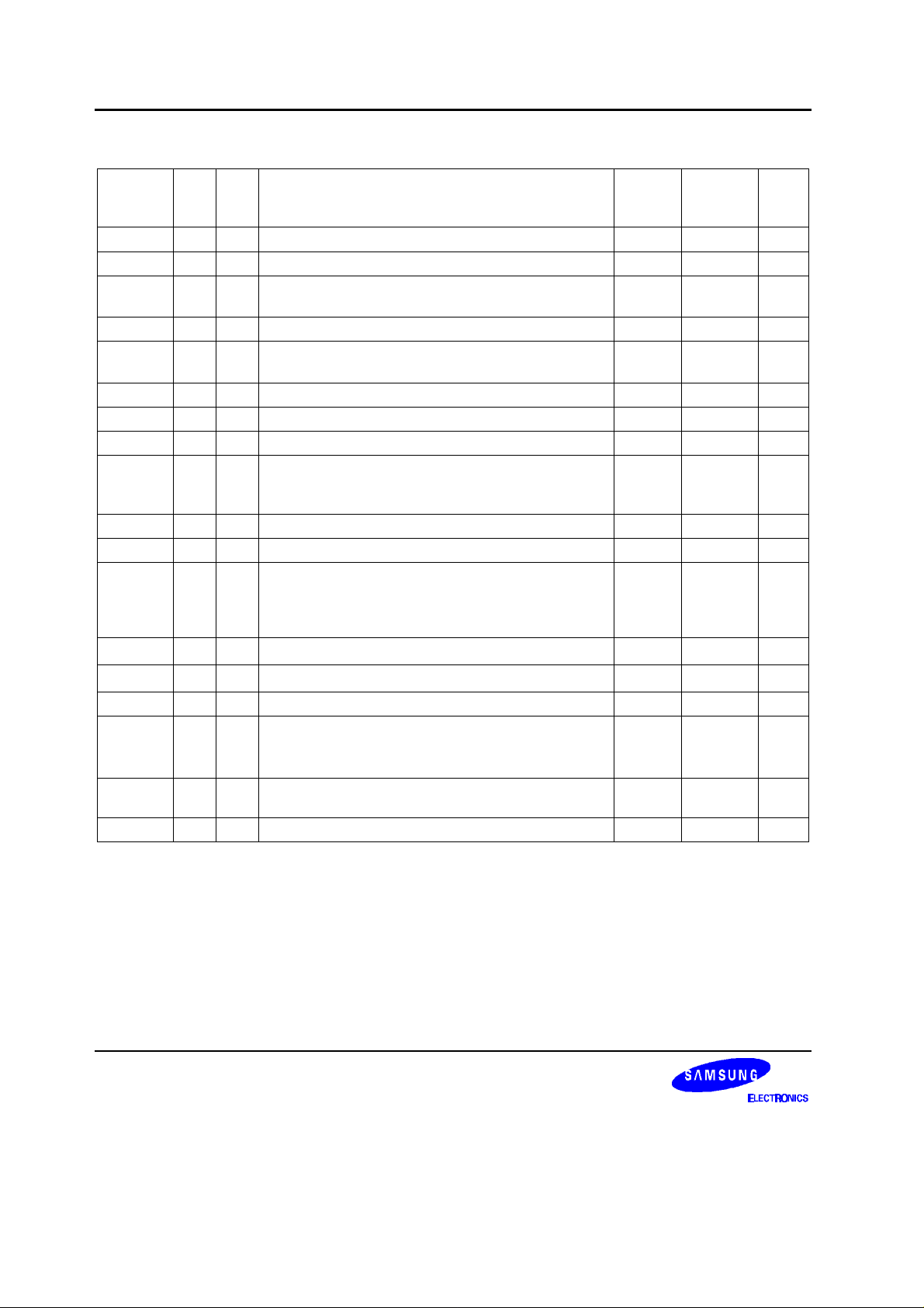
PIN DESCRIPTIONS
Table 1-1. KS57C5204/C5208 Pin Descriptions
Pin
Name
P1.0
P1.1
P1.2
P1.3
P2.0
P2.1
P2.2
P2.3
P3.0
P3.1
P3.2
P3.3
P4.0
P4.1
P4.2
P4.3
P5.0-P5.3
P6.0-P6.3
P7.0-P7.3
P8.0-P8.3
P9.0-P9.2
Pin
Reset
Type
Value
I I 4-bit input port.
1-bit and 4-bit read and test is possible.
Each pull-up resistors are assignable by software.
I/O I 4-bit I/O port.
1-bit and 4-bit read/write and test is possible.
Individual pins are software configurable as input or
output.
4-bit pull-up resistors are software assignable to input
pins and are automatically disabled for output pins.
Ports 2 and 3 can be paired to enable 8-bit data
transfer.
I/O I 4-bit I/O ports.
1-bit and 4-bit read/write and test is possible.
Individual pins are software configurable as input or
output.
4-bit pull-up resistors are software assignable to input
pins and are automatically disabled for output pins.
N-channel open-drain or push-pull output can be
selected by software (1-bit unit)
Ports 4 and 5 can be paired to support 8-bit data
transfer.
I/O I 4-bit I/O ports.
1-bit or 4-bit read/write and test is possible.
Individual pins are software configurable as input or
output.
4-bit pull-up resistors are software assignable to input
pins and are automatically disabled for output pins.
Ports 6 and 7 can be paired to enable 8-bit data
transfer.
I/O I 4-bit I/O port.
1-bit or 4-bit read/write and test is possible.
Individual pins are software configurable as input or
output.
4-bit pull-up resistors are software assignable to input
pins and are automatically disabled for output pins.
Ports 8 and 9 can be paired to enable 8-bit data
transfer.
Description Pin
Number
1 (39)
2 (40)
3 (41)
4 (42)
5 (43)
6 (44)
7 (1)
8 (2)
9 (3)
10 (4)
19 (13)
20 (14)
16 (10)
17 (11)
21 (15)
22 (17)
27-30
(22-25)
31-34
(26-29)
35-38
(30-33)
23-26
(18-21)
40-42
(35-37)
Share
Pin
INT0
INT1
INT2
INT4
TCLO0
TCLO1
CLO
BUZ
TCL0
TCL1
BTCO E-2
KS0-KS3
KS4-KS7
– D-2
Type
A-4
D-2
D-4
D-4
1-7
PRODUCT OVERVIEW KS57C5204/C5208/P5208/C5304/C5308/P5308/C5312/P5312
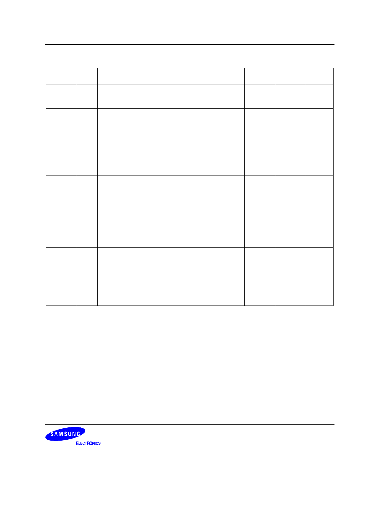
Table 1-1. KS57C5204/C5208 Pin Descriptions (Continued)
Pin Name Pin
Type
Reset
Value
Description Pin
Number
Share
Pin
Circu
it
Type
DTMF O – DTMF output. 39 (34) – G-6
BTCO I/O I Basic timer clock output 16 (10) P4.0 E-2
INT0
INT1
I I External interrupts. The triggering edge for INT0 and
INT1 is selectable.
1 (39)
2 (40)
P1.0
P1.1
A-4
INT2 I I Quasi-interrupt with detection of rising edges 3 (41) P1.2 A-4
INT4 I I External interrupt with detection of rising and falling
4 (42) P1.3 A-4
edges.
TCLO0 I/O I Timer/counter 0 clock output 5 (43) P2.0 D-2
TCLO1 I/O I Timer/counter 1 clock output 6 (44) P2.1 D-2
CLO I/O I Clock output 7 (1) P2.2 D-2
BUZ I/O I 2 kHz, 4 kHz, 8 kHz, or 16 kHz frequency output at the
8 (2) P2.3 D-2
watch timer clock frequency of 4.19 MHz for buzzer
sound
TCL0 I/O I External clock input for timer/counter 0 9 (3) P3.0 D-4
TCL1 I/O I External clock input for timer/counter 1 10 (4) P3.1 D-4
KS0-KS3
KS4-KS7
I/O I Quasi-interrupt inputs with falling edge detection 31-34
(26-29)
35-38
P6.0-P6.3
P7.0-P7.3
D-4
(30-33)
V
DD
V
SS
RESET
X
IN
X
OUT
TEST – – Chip test input pin, Hold GND when the device is
– – Power supply 11 (5) – –
– – Ground 12 (6) – –
– – RESET signal 18 (12) – B
– – Crystal, or ceramic oscillator signal for main system
clock. (For external clock input, use XIN and input XIN's
reverse phase to X
OUT
)
14 (8)
13 (7)
– –
15 (9) – –
operating.
NC – – No connection (16, 38) – –
NOTE: Parentheses indicate pin number for 44 QFP package.
1-8
KS57C5204/C5208/P5208/C5304/C5308/P5308/C5312/P5312PRODUCT OVERVIEW
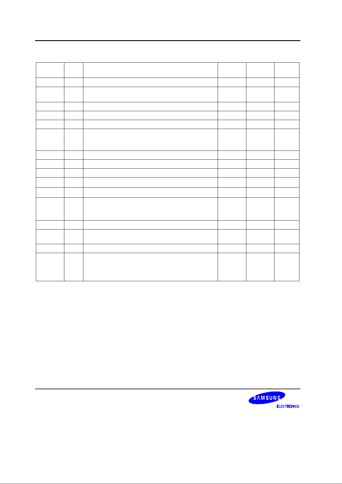
Table 1-2. KS57C5304/C5308/C5312 Pin Descriptions
Pin
Name
Pin
Type
P1.0 I 1-bit input port.
1-bit and 4-bit read and test is possible.
Each bit pull-up resistors are assignable.
P2.0
P2.1
P2.2
P2.3
I/O 4-bit I/O port.
1-bit and 4-bit read/write and test is possible.
Each individual pin can be assignable as input or
output. 4-bit pull-up resisters are software assignable to
input pins and are automatically disabled for output
pins.
P3.0
P3.1
P4.0
P4.1
P4.2
P4.3
P5.0-P5.3
Ports 2 and 3 can be paired to enable 8-bit data
transfer.
I/O 4-bit I/O ports.
1-bit and 4-bit read/write and test is possible.
Each individual pin can be assignable as input or
output. 4-bit pull-up resisters are software assignable to
input pins and are automatically disabled for output
pins.
The N-channel open-drain or push-pull output can be
selected by software (1-bit unit).
Ports 4 and 5 can be paired to enable 8-bit data
transfer.
P6.0-P6.3
I/O 4-bit I/O ports.
1-bit and 4-bit read/write and test is possible.
P7.0-P7.3
Each individual pin can be assignable as input or
output. 4-bit pull-up resisters are software assignable to
input pins and are automatically disabled for output
pins.
Ports 6 and 7 can be paired to enable 8-bit data
transfer.
Description Pin
Number
23 (25) INT0 A-4
24 (26)
25 (27)
26 (28)
27 (29)
28 (30)
29 (31)
5 (5)
6 (6)
8 (8)
9 (10)
10-13
(11-14)
14-17
(15-18)
18-21
(19-22)
Share
Circuit
Pin
TCLO0
TCLO1
CLO
BUZ
TCL0
TCL1
BTCO E-2
KS0-KS3
KS4-KS7
Type
D-2
D-4
D-4
1-9
PRODUCT OVERVIEW KS57C5204/C5208/P5208/C5304/C5308/P5308/C5312/P5312
Table 1-2. KS57C5304/C5308/C5312 Pin Descriptions (Continued)
Pin Name I/O
Type
Description Pin
Number
Share
Pin
Circuit
Type
DTMF O DTMF output. 22 (23) – G-6
INT0 I External interrupt input.
23 (25) P1.0 A-3
The triggering edge for INT0 is selectable.
TCLO0 I/O Timer/counter 0 clock output 24 (26) P2.0 D-2
TCLO1 I/O Timer/counter 1 clock output 25 (27) P2.1 D-2
CLO I/O Clock output 26 (28) P2.2 D-2
BUZ I/O 2 kHz, 4 kHz, 8 kHz, or 16 kHz frequency output at the
27 (29) P2.3 D-2
watch timer clock frequency of 4.19 MHz for buzzer
sound
TCL0 I/O External clock input for timer/counter 0 28 (30) P3.0 D-4
TCL1 I/O External clock input for timer/counter 1 29 (31) P3.1 D-4
BTCO I/O Basic timer clock output 5 (5) P4.0 E-2
V
V
X
X
DD
SS
IN
OUT
– Power supply 30 (32) – –
– Ground 1 (1) – –
– Crystal, or ceramic oscillator signal for main system
clock. (For external clock input, use XIN and input XIN's
reverse phase to X
OUT
)
3 (3)
2 (2)
– –
NC – No connection (9, 24) – –
TEST – Chip test input pin, Hold GND when the device is
4 (4) – –
operating.
RESET
KS0-KS3
KS4-KS7
– RESET signal 7 (7) – B
I/O Quasi-interrupt inputs with falling edge detection 14-17
(15-18)
P6.0-P6.3
P7.0-P7.3
18-21
D-4
(19-22)
NOTE: Parentheses indicate the pin number for 32-SOP package.
1-10

KS57C5204/C5208/P5208/C5304/C5308/P5308/C5312/P5312PRODUCT OVERVIEW
PIN CIRCUIT DIAGRAMS
V
DD
V
DD
P-Channel
In
N-Channel
Figure 1-6. Pin Circuit Type A
V
DD
Pull-Up
Resistor
P-Channel
In
Schmitt Trigger
Resistor
Enable
Data
Output
DIsable
Pull-Up
Resistor
In
Schmitt Trigger
Figure 1-8. Pin Circuit Type B
V
DD
P-Channel
N-Channel
Out
Figure 1-7. Pin Circuit Type A-4
Figure 1-9. Pin Circuit Type C
1-11

PRODUCT OVERVIEW KS57C5204/C5208/P5208/C5304/C5308/P5308/C5312/P5312
DTMF Out
V
VDD
DD
Pull-up
Enable
Data
Output
DIsable
Circuit
Type C
Figure 1-10. Pin Circuit Type D-2
VDD
Pull-up
Enable
Pull-up
Resistor
P-Channel
I/O
Pull-up
Resistor
P-Channel
PNE
Data
Output
Disable
P-Channel
N-Channel
Figure 1-12. Pin Circuit Type E-2
V
DD
Resistor
Pull-up
Resistor
Enable
I/O
Pull-up
1-12
Data
Output
Disable
Circuit
Type C
Schmitt Trigger
Figure 1-11. Pin Circuit Type D-4
I/O
Output
Disable
Figure 1-13. Pin Circuit Type G-6
 Loading...