

Samsung KS57P4104, KS57C4204, KS57C4104, KS57P4304, KS57P4204 Datasheet
...
KS57C4104/P4104/C4204/P4204/C4304/P4304 PRODUCT OVERVIEW
1 PRODUCT OVERVIEW
OVERVIEW
The KS57C4104/KS57C4204/KS57C4304 single-chip CMOS microcontroller has been designed for very high
performance using Samsung's newest 4-bit CPU core, SAM47 (Samsung Arrangeable Microcontroller).
With an A/D converter, LED direct drive pins, an 8-bit serial I/O interface, and an 8-bit timer/counter, the
KS57C4104/KS57C4204/KS57C4304 offers you an excellent design solution for a wide variety of home
appliance applications — electric fans, cookers, boilers, and air conditioners, for example.
Up to 35 pins of the 42-pin SDIP or 44-pin QFP package can be dedicated to I/O. Seven vectored interrupts
provide fast response to internal and external events.
In addition, the KS57C4104/KS57C4204/KS57C4304's advanced CMOS technology provides for low power
consumption and a wide operating voltage range.
OTP
The KS57C4104/KS57C4204/KS57C4304 microcontroller is also available in OTP (One Time Programmable)
version, KS57P4104/KS57P4204/KS57P4304. KS57P4104/KS57P4204/KS57P4304 microcontroller has an onchip 4-Kbyte one-time-programmable EPROM instead of masked ROM. The
KS57P4104/KS57P4204/KS57P4304 is comparable to KS57C4104/KS57C4204/KS57C4304, in function, in D.C.
electrical characteristics and in pin configuration.
DEVELOPMENT SUPPORT
The Samsung Microcontroller Development System, SMDS, provides you with a complete PC-based development environment for KS57-series microcontrollers that is powerful, reliable, and portable. In addition to its
window-based program development structure, the SMDS toolset includes versatile debugging, trace, instruction
timing, and performance measurement applications.
The Samsung Generalized Assembler (SAMA) has been designed specifically for the SMDS environment and
accepts assembly language sources in a variety of microprocessor formats. SAMA generates industry-standard
hex files that also contain program control data for SMDS compatibility.
1-1

PRODUCT OVERVIEW KS57C4104/P4104/C4204/P4204/C4304/P4304
FEATURES SUMMARY
Memory
• 256 × 4-bit RAM
• 4,096 × 8-bit ROM
35 I/O Pins
• I/O: 31 pins including 8 LED direct drive pins
(KS57C4104/C4304)
18 pins including 8 LED direct drive pins
(KS57C4204)
• Input only: 4 pins
A/D Converter
• 6-channel with 8-bit resolution
• 22.89 µs conversion speed at 4.19 MHz
Basic Timer
• One 8-bit basic timer
• Watchdog timer functions
• Four interval clock selection
Timer/Counters
• Two 8-bit timer/counter (TC0, TC1)
• Programmable 8-bit timer
• External event counter
• Arbitrary clock frequency output
• PWM output mode (TC1)
Watch Timer
• One watch timer 8-bit
• Time interval generation: 0.5 s, 3.9 ms at
4.19 MHz
• Four frequency outputs to BUZ pin
Built-in reset circuit (KS57C4304 only)
• Built-in power-on reset circuit
Interrupts
• Five internal vectored interrupts
(INTB, INTT0, INTT1, INTS, INTAD)
• Three external vectored interrupts
(INT0, INT1, INT4)
• Two quasi-interrupts (INT2, INTW)
Bit Sequential Carrier
• Supports 16-bit serial data transfer in
arbitrary format
Memory-Mapped I/O Structure
• Data memory bank 15
Two Power-Down Modes
• Idle mode (only CPU clock stops)
• Stop mode (system oscillation stops)
Oscillation Sources
• Crystal, Ceramic, or RC for system clock
• Crystal, Ceramic: 0.4–6.0 MHz
• RC: 4 MHz (typ)
• CPU clock divider circuit (by 4, 8, or 64)
Instruction Execution Times
• 0.95, 1.91, 15.3 µs at 4.19 MHz
• 0.67, 1.33, 10.7 µs at 6.0 MHz
Operating Temperature
• – 40 °C to 85 °C
8-bit Serial I/O Interface
• 8-bit transmit/receive mode
• 8-bit receive mode
• LSB-first or MSB-first transmission selectable
• Internal or external clock source
1-2
Operating Voltage Range
• 1.8 V to 5.5 V (KS57C4104/C4204)
• 2.5 V to 5.5 V (KS57C4304)
Package Type
• 42-pin SDIP, 44-pin QFP (KS57C4104/C4304)
30-pin SDIP, 28-pin SOP (KS57C4204)

KS57C4104/P4104/C4204/P4204/C4304/P4304 ELECTRICAL DATA
14 ELECTRICAL DATA
OVERVIEW
In this section, information on KS57C4104/C4204/C4304 electrical characteristics is presented as tables and
graphics. The information is arranged in the following order:
Standard Electrical Characteristics
— Absolute maximum ratings
— D.C. electrical characteristics
— System clock oscillator characteristics
— Operating voltage range
— A.C. electrical characteristics
— A/D converter electrical characteristics
— I/O capacitance
Stop Mode Characteristics and Timing Waveforms
— RAM data retention supply voltage in stop mode
— Stop mode release timing when initiated by RESET
— Stop mode release timing when initiated by an interrupt request
Miscellaneous Timing Waveforms
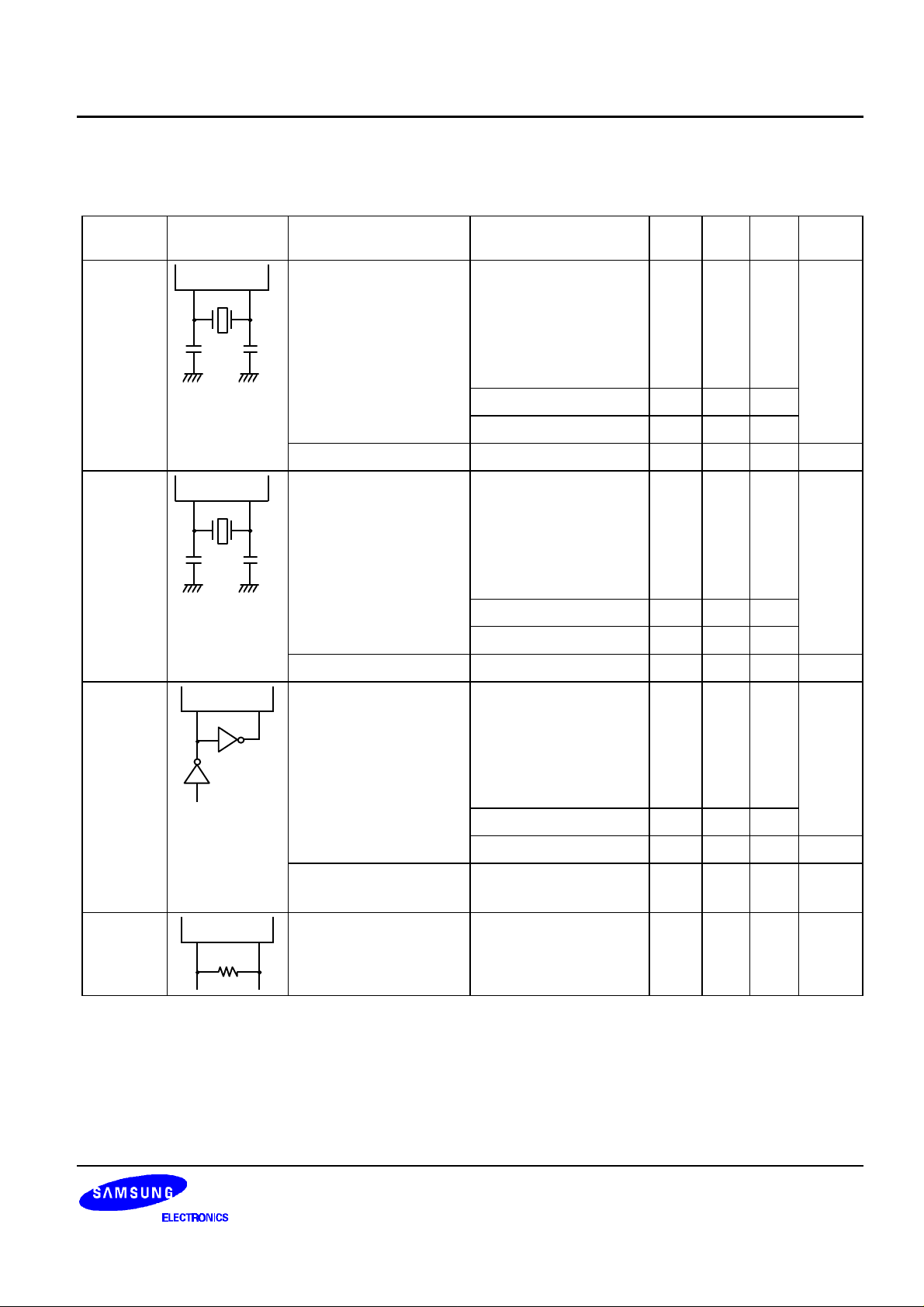
— A.C timing measurement points (except for XIN)
— Clock timing measurement at X
— TCL0/1 timing
— Input timing for RESET signal
— Input timing for external interrupts and quasi-interrupts
— KS57C4304 power-on RESET timing
— Serial data transfer timing
IN
14-1

ELECTRICAL DATA KS57C4104/P4104/C4204/P4204/C4304/P4304
Table 14-1. KS57C4104/C4204 Absolute Maximum Ratings
(T
= 25 °C)
A
Parameter Symbol Conditions Rating Units
Supply Voltage
Input Voltage
Output Voltage
Output Current High
V
DD
I
V
V
OH
O
All I/O ports
I
One pin – 15 mA
– – 0.3 to + 6.5 V
– 0.3 to V
–
– 0.3 to VDD + 0.3
DD
+ 0.3
V
V
All output pins – 35
Output Current Low
I
OL
One pin
peak value
(note)
+ 30 mA
rms value + 15
All pins
peak value
(note)
+ 100
rms value + 60
Operating Temperature
Storage Temperature
T
A
T
stg
– – 40 to + 85
– – 65 to + 150
°
C
°
C
NOTE: The values for Output Current Low (IOL) are calculated as Peak Value × Duty .
14-2
KS57C4104/P4104/C4204/P4204/C4304/P4304 ELECTRICAL DATA
Table 14-2. KS57C4104/C4204 D.C. Electrical Characteristics
(T
= – 40 °C to + 85 °C, VDD = 1.8 V to 5.5 V)
A
Parameter Symbol Conditions Min Typ Max Units
Input High
Voltage
Input Low
Voltage
Output High
Voltage
V
IH1
V
IH2
V
IH3
V
V
V
V
OH
IL1
IL2
IL3
All input pins except those specified
below for V
IH2–VIH3
Ports 0, 1, 3, 6 and RESET
X
IN, XOUT
All input pins except those specified
below for V
IL2–VIL3
Ports 0, 1, 3, 6 and RESET
X
IN, XOUT
VDD = 4.5 V to 5.5 V
IOH = – 1 mA
0.7 V
DD
0.8 V
DD
V
– 0.1 V
DD
–
– –
V
DD
– 1.0
– – V
V
DD
V
DD
DD
0.3 V
0.2 V
0.1
DD
DD
V
V
Ports 0, 2–8
Output Low
Voltage
V
OL
V
= 4.5 V to 5.5 V
DD
I
= 15 mA
OL
– 0.4 2 V
Ports 4 and 5 only
I
OL
= 4 mA
0.2
All output ports except ports 4 and 5
Input High
Leakage Current
Input Low
Leakage Current
Output High
Leakage Current
Output Low
Leakage Current
Pull-up Resistor
Pull-up Resistor
I
LIH1
I
LIH2
I
LIL1
I
LIL2
I
LOH
I
LOL
R
R
VI = V
DD
All input pins except those specified
below for I
VI = V
XIN and X
DD
LIH2
OUT
only
VI = 0 V
All input pins except XIN and X
RESET
V
= 0 V
I
X
V
IN
O
and X
= V
DD
OUT
only
All output pins
V
= 0 V
O
All output pins
V
L1
L2
= 0 V; V
I
V
= 0 V; V
I
V
= 0 V; V
I
V
= 0 V; V
I
= 5 V except RESET
DD
= 3 V except RESET
DD
= 5 V; RESET
DD
= 3 V; RESET
DD
OUT
– – 3 µA
20
– – – 3 µA
,
– 20
– – 3 µA
– – – 3 µA
25 50 100
kΩ
50 100 200
100 250 400
kΩ
200 500 800
14-3
ELECTRICAL DATA KS57C4104/P4104/C4204/P4204/C4304/P4304
Table 14-2. KS57C4104/C4204 D.C. Electrical Characteristics (Continued)
(T
= – 40 °C to + 85 °C, VDD = 1.8 V to 5.5 V)
A
Parameter Symbol Conditions Min Typ Max Units
Supply
Current
(1)
I
DD1
Run mode; V
= 5.0 V ± 10%
DD
6.0MHz – 3.0 8.0
Crystal oscillator; C1=C2=22pF 4.19MHz 2.3 5.5
V
= 3 V ± 10%
DD
6.0MHz 1.4 4.0
mA
4.19MHz 1.1 3.0
I
DD2
Idle mode; V
= 5.0 V ± 10%
DD
6.0MHz – 1.1 2.5
mA
Crystal oscillator; C1=C2=22pF 4.19MHz 1.0 1.8
V
= 3 V ± 10%
DD
6.0MHz 0.5 1.5
4.19MHz 0.4 1.0
I
DD3
NOTES:
1. D.C. electrical values for Supply current (I
output port drive currents and ADC.
2. The supply current assumes a CPU clock of fx/4.
Stop mode; V
Stop mode; V
= 5.0 V ± 10%
DD
= 3.0 V ± 10%
DD
to I
DD1
) do not include current drawn through internal pull-up registers,
DD3
– 0.1 5.0
0.1 3.0
µA
14-4
KS57C4104/P4104/C4204/P4204/C4304/P4304 ELECTRICAL DATA
Table 14-3. KS57C4104/C4204 System Clock Oscillator Characteristics
(T
= – 40 °C to + 85 °C, VDD = 1.8 V to 5.5 V)
A
Oscillator Clock
Configuration
Ceramic
Xin Xout
Oscillator
C1 C2
Crystal
Xin Xout
Oscillator
C1 C2
External
Xin Xout
Clock
Parameter Test Condition Min Typ Max Units
Oscillation frequency
Stabilization time
(2)
Oscillation frequency
Stabilization time
(2)
XIN input frequency
(1)
VDD = 2.7 V to 5.5 V
VDD = 2.0 V to 5.5 V
VDD = 1.8 V to 5.5 V
VDD = 3.0 V
(1)
VDD = 2.7 V to 5.5 V
VDD = 2.0 V to 5.5 V
VDD = 1.8 V to 5.5 V
VDD = 3.0 V
(1)
VDD = 2.7 V to 5.5 V
0.4 – 6.0 MHz
0.4 – 4.2
0.4 – 3.0
– – 4 ms
0.4 – 6.0 MHz
0.4 – 4.2
0.4 – 3.0
– – 10 ms
0.4 – 6.0 MHz
XIN input high and low
VDD = 2.0 V to 5.5 V
VDD = 1.8 V to 5.5 V
– 83.3 – 1250 ns
0.4 – 4.2
0.4 – 3.0
level width (tXH, tXL)
RC
Xin Xout
Oscillator
R
NOTES:
1. Oscillation frequency and Xin input frequency data are for oscillator characteristics only.
2. Stabilization time is the interval required for oscillating stabilization after a power-on occurs, or when stop mode is
terminated.
Oscillation frequency
limitation
VDD = 5 V
R = 8.2 KΩ
– 4 – MHz
14-5

ELECTRICAL DATA KS57C4104/P4104/C4204/P4204/C4304/P4304
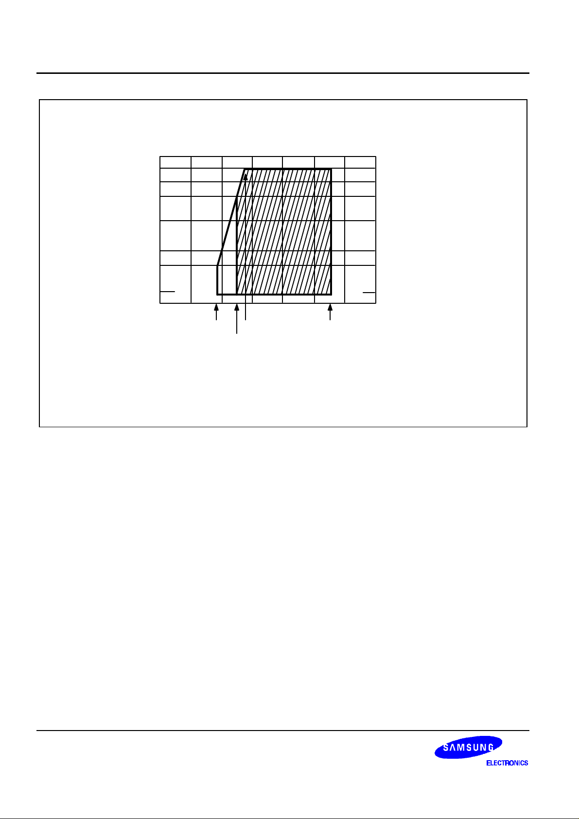
Main Oscillator Frequency
CPU CLOCK
1.5 MHz
(Divided by 4)
6 MHz
1.05 MHz
0.75 MHz
15.6 kHz
1 2 3 4 5 6
2.7 5.5
1.8
SUPPLY VOLTAGE (V)
CPU CLOCK = 1/n x oscillator frequency (n = 4, 8 or 64)
4.2 MHz
3 MHz
Figure 14-1. KS57C4104/C4204 Standard Operating Voltage Range
Table 14-4. KS57C4104/C4204 A.C. Electrical Characteristics
(TA = – 40 °C to + 85 °C, V
= 1.8 V to 5.5 V)
DD
Parameter Symbol Conditions Min Typ Max Units
Instruction Cycle
Time
t
CY
V
= 2.7 V to 5.5 V
DD
VDD = 1.8 V to 5.5 V
0.67 – 64
1.33
µs
TCL0/1 Input
Frequency
TCL0/1 Input High,
Low Width
SCK Cycle Time
14-6
f
TI
t
TIH, tTIL
t
KCY
V
= 2.7 V to 5.5 V
DD
0 – 1.5 MHz
VDD = 1.8 V to 5.5 V
V
= 2.7 V to 5.5 V
DD
VDD = 1.8 V to 5.5 V
VDD = 2.7 V to 5.5 V
0.48 – –
1.8
800 – – ns
External SCK source
Internal SCK source 670
VDD = 1.8 V to 5.5 V
3200
External SCK source
Internal SCK source 3800
0.75 MHz
µs

KS57C4104/P4104/C4204/P4204/C4304/P4304 ELECTRICAL DATA
Table 14-4. KS57C4104/C4204 A.C. Electrical Characteristics (Continued)
(TA = – 40 °C to + 85 °C, V
= 1.8 V to 5.5 V)
DD
Parameter Symbol Conditions Min Typ Max Units
SCK High, Low
Width
tKH, t
VDD = 2.7 V to 5.5 V
KL
External SCK source
Internal SCK source
VDD = 1.8 V to 5.5 V
335 – – ns
t
/2 – 50
KCY
1600
External SCK source
SI Setup Time to
SCK High
t
SIK
Internal SCK source
VDD = 2.7 V to 5.5 V
External SCK source
t
/2 – 150
KCY
100 – – ns
Internal SCK source 150
VDD = 1.8 V to 5.5 V
150
External SCK source
Internal SCK source 500
SI Hold Time to
SCK High
t
KSI
VDD = 2.7 V to 5.5 V
External SCK source
400 – – ns
Internal SCK source 400
VDD = 1.8 V to 5.5 V
600
External SCK source
Internal SCK source 500
(1)
Output Delay for
SCK to SO
t
KSO
VDD = 2.7 V to 5.5 V
External SCK source
– – 300 ns
Internal SCK source 250
VDD = 1.8 V to 5.5 V
1000
External SCK source
Internal SCK source 1000
Interrupt Input
High, Low Width
t
INTH
t
INTL
,
INT0
(2)
– –
INT1, INT2, INT4, KS0–KS3 10
RESET Input Low
t
RSL
Input 10 – –
Width
µs
µs
NOTES:
1. R(1KΩ) and C (100pF) are the load resistance and load capacitance of the SO output line.
2. Minimum value for INT0 is based on a clock of 2tCY or 128/fx as assigned by the IMOD0 register setting.
14-7

ELECTRICAL DATA KS57C4104/P4104/C4204/P4204/C4304/P4304
Table 14-5. KS57C4304 Absolute Maximum Ratings
(T
= 25 °C)
A
Parameter Symbol Conditions Rating Units
Supply Voltage
Input Voltage
Output Voltage
Output Current High
V
DD
I
V
V
OH
O
All I/O ports
I
One pin – 15 mA
– – 0.3 to + 6.5 V
– 0.3 to V
–
– 0.3 to VDD + 0.3
DD
+ 0.3
V
V
All output pins – 35
Output Current Low
I
OL
One pin
peak value
(note)
+ 30 mA
rms value + 15
All pins
peak value
(note)
+ 100
rms value + 60
Operating Temperature
Storage Temperature
T
A
T
stg
– – 40 to + 85
– – 65 to + 150
°
C
°
C
NOTE: The values for Output Current Low (IOL) are calculated as Peak Value × Duty .
14-8

KS57C4104/P4104/C4204/P4204/C4304/P4304 ELECTRICAL DATA
Table 14-6. KS57C4304 D.C. Electrical Characteristics
(T
= – 40 °C to + 85 °C, VDD = 2.5 V to 5.5 V)
A
Parameter Symbol Conditions Min Typ Max Units
Input High
Voltage
Input Low
Voltage
Output High
Voltage
V
IH1
V
IH2
V
IH3
V
IL1
V
IL2
V
IL3
V
OH
All input pins except those specified
below for V
IH2–VIH3
Ports 0, 1, 3, 6 and RESET
X
IN, XOUT
All input pins except those specified
below for V
IL2–VIL3
Ports 0, 1, 3, 6 and RESET
X
IN, XOUT
VDD = 4.5 V to 5.5 V
IOH = – 1 mA
0.7 V
DD
0.8 V
DD
V
– 0.1 V
DD
–
– –
V
DD
– 1.0
– – V
V
DD
V
DD
DD
0.3 V
0.2 V
0.1
DD
DD
V
V
Ports 0, 2–8
Output Low
Voltage
V
OL
V
I
DD
OL
= 3.5 V
= 15 mA
– 0.4 2 V
Ports 4 and 5 only
I
OL
= 4 mA
0.2
All output ports except ports 4 and 5
Input High
Leakage Current
Input Low
Leakage Current
Output High
Leakage Current
Output Low
Leakage Current
Pull-Up Resistor
Pull-Up Resistor
I
LIH1
I
LIH2
I
LIL1
I
LIL2
I
LOH
I
LOL
R
R
L1
L2
VI = V
DD
All input pins except those specified
below for I
VI = V
XIN and X
DD
LIH2
OUT
only
VI = 0 V
All input pins except XIN and X
RESET
V
= 0 V
I
X
V
IN
O
= V
and X
DD
OUT
only
OUT,
All output pins
V
= 0 V
O
All output pins
V
= 0 V; V
I
V
= 0 V; V
I
V
= 0 V; V
I
V
= 0 V; V
I
= 5 V except RESET
DD
= 3 V except RESET
DD
= 5 V; RESET
DD
= 3 V; RESET
DD
– – 3 µA
20
– – – 3 µA
– 20
– – 3 µA
– – – 3 µA
25 50 100
50 100 200
100 250 400
200 500 800
kΩ
kΩ
14-9

ELECTRICAL DATA KS57C4104/P4104/C4204/P4204/C4304/P4304
Table 14-6. KS57C4304 D.C. Electrical Characteristics (Continued)
(T
= – 40 °C to + 85 °C, VDD = 2.5 V to 5.5 V)
A
Parameter Symbol Conditions Min Typ Max Units
Supply
Current
(1)
I
DD1
Run mode; V
= 5.0 V ± 10%
DD
6.0MHz – 3.1 8.0
Crystal oscillator; C1 = C2 = 22pF 4.19MHz 2.4 5.5
V
= 3 V ± 10%
DD
6.0MHz 1.5 4.0
mA
4.19MHz 1.2 3.0
I
DD2
Idle mode; V
= 5.0 V ± 10%
DD
6.0MHz – 1.2 2.5
mA
Crystal oscillator; C1 = C2 = 22pF 4.19MHz 1.1 1.8
V
= 3 V ± 10%
DD
6.0MHz 0.6 1.5
4.19MHz 0.5 1.0
I
DD3
NOTES:
1. D.C. electrical values for Supply current (I
output port drive currents and ADC.
2. The supply current assumes a CPU clock of fx/4.
Stop mode; V
Stop mode; V
= 5.0 V ± 10%
DD
= 3.0 V ± 10%
DD
to I
DD1
) do not include current drawn through internal pull-up registers,
DD3
– 120 200
100 150
µA
Table 14-7. KS57C4304 Power-On Reset Circuit Characteristics
(T
= – 40 °C to + 85 °C, VDD = 2.5 V to 5.5 V)
A
Parameter Symbol Conditions Min Typ Max Units
Power-On Reset
V
DDH
Voltage High
Power-On Reset
V
DDL
Voltage Low
Power Supply
t
r
Voltage Rise Time
Power Supply
t
off
Voltage Off Time
I
Power-On Reset Circuit
Cunsumption Current
NOTES:
1. 217/fx (= 31.3 ms at fx = 4.19 MHz)
2. Current consumed when power-on reset circuit is provided internally.
(2)
DDPR
V
= 5 V ± 10%
DD
V
= 3 V ± 10%
DD
2.5 5.5 V
0 2.0 2.2 V
10
(1)
us
0.5 s
120 200 uA
100 150 uA
14-10

KS57C4104/P4104/C4204/P4204/C4304/P4304 ELECTRICAL DATA
Table 14-8. KS57C4304 System Clock Oscillator Characteristics
(T
= – 40 °C to + 85 °C, VDD = 2.5 V to 5.5 V)
A
Oscillator Clock
Configuration
Ceramic
Xin Xout
Oscillator
C1 C2
Crystal
Xin Xout
Oscillator
C1 C2
External
Xin Xout
Clock
Parameter Test Condition Min Typ Max Units
Oscillation frequency
Stabilization time
(2)
Oscillation frequency
Stabilization time
(2)
XIN input frequency
(1)
VDD = 2.7 V to 5.5 V
VDD = 2.5 V to 5.5 V
VDD = 3.0 V
(1)
VDD = 2.7 V to 5.5 V
VDD = 2.5 V to 5.5 V
VDD = 3.0 V
(1)
VDD = 2.7 V to 5.5 V
0.4 – 6.0 MHz
0.4 – 4.2
– – 4 ms
0.4 – 6.0 MHz
0.4 – 4.2
– – 10 ms
0.4 – 6.0 MHz
XIN input high and low
VDD = 2.5 V to 5.5 V
– 83.3 – 1250 ns
0.4 – 4.2
level width (tXH, tXL)
RC
Oscillator
NOTES:
1. Oscillation frequency and Xin input frequency data are for oscillator characteristics only.
2. Stabilization time is the interval required for oscillating stabilization after a power-on occurs, or when stop mode is
terminated.
Xin Xout
R
Oscillation frequency
limitation
VDD = 5 V
R = 8.2 KΩ
– 4 – MHz
14-11
ELECTRICAL DATA KS57C4104/P4104/C4204/P4204/C4304/P4304
Main Oscillator Frequency
CPU CLOCK
1.5 MHz
(Divided by 4)
6 MHz
1.05 MHz
0.75 MHz
15.6 kHz
1 2 3 4 5 6
1.8
2.7 5.5
2.5
SUPPLY VOLTAGE (V)
CPU CLOCK = 1/n x oscillator frequency (n = 4, 8 or 64)
Figure 14-2. KS57C4304 Standard Operating Voltage Range
4.2 MHz
3 MHz
14-12
KS57C4104/P4104/C4204/P4204/C4304/P4304 ELECTRICAL DATA
Table 14-9. KS57C4304 A.C. Electrical Characteristics
(T
= – 40 °C to + 85 °C, V
A
= 2.5 V to 5.5 V)
DD
Parameter Symbol Conditions Min Typ Max Units
Instruction Cycle
t
CY
VDD = 2.7 V to 5.5 V
0.67 – 64 µs
Time
TCL0/1 Input
f
TI0
VDD = 2.7 V to 5.5 V
0 – 1.5 MHz
Frequency
TCL0/1 Input
TIH0
, t
TIL0VDD
= 2.7 V to 5.5 V
0.48 – – µs
t
High, Low Width
SCK Cycle Time
t
KCY
VDD = 2.7 V to 5.5 V
800 – – ns
External SCK source
Internal SCK source 670
SCK High, Low
Width
SI Setup Time to
SCK High
tKH, t
t
SIK
VDD = 2.7 V to 5.5 V
KL
External SCK source
Internal SCK source
VDD = 2.7 V to 5.5 V
External SCK source
325 – – ns
t
/2 – 50
KCY
100 – – ns
Internal SCK source 150
SI Hold Time to
SCK High
t
KSI
V
= 2.7 V to 5.5 V
DD
External SCK source
400 – – ns
Internal SCK source 400
Output Delay for
SCK to SO
t
KSO
VDD = 2.7 V to 5.5 V
External SCK source
– – 300 ns
Internal SCK source 250
t
Interrupt Input
High, Low Width
RESET Input
INTH
t
INTL
t
RSL
,
INT0
(NOTE)
– – µs
INT1, INT2, INT4, KS0–KS3 10
Input 10 – – µs
Low Width
NOTE: Minimum value for INT0 is based on a clock of 2t
or 128/fx as assigned by the IMOD0 register setting.
CY
14-13

ELECTRICAL DATA KS57C4104/P4104/C4204/P4204/C4304/P4304
Table 14-10. A/D Converter Electrical Characteristics
(T
= – 10 °C to + 70 °C, VDD = 3.5 V to 5.5 V, VSS = AVSS = 0 V)
A
Parameter Symbol Condition Min Typ Max Units
Resolution – – 8 8 8 bit
Absolute accuracy
Conversion time
(1)
(2)
Analog input voltage
Analog input impedance
NOTES:
1. Absolute accuracy does not include the quantization error (± 1/2 LSB).
2. Conversion time is the time required from the moment a conversion operation starts until it ends (EOC = 0).
3. 'fx' is the abbreviation for system clock.
t
CON
V
R
–
IAN
AN
2.5 V < AV
< V
REF
DD
– –
–
– –
AV
SS
96/fx
–
± 1.5
(3)
AV
– – 1000 –
LSB
– µs
REF
V
MΩ
Table 14-11. Input/Output Capacitance
(TA = 25 °C, V
DD
= 0 V )
Parameter Symbol Condition Min Typ Max Units
C
C
OUT
IN
f = 1 MHz; Unmeasured pins
are returned to V
SS
– – 15 pF
– – 15 pF
Input
Capacitance
Output
Capacitance
I/O Capacitance
C
IO
– – 15 pF
Table 14-12. RAM Data Retention Supply Voltage in Stop Mode
(TA = – 40 °C to + 85 °C)
Parameter Symbol Conditions Min Typ Max Unit
(1)
V
DDDR
I
DDDR
t
SREL
t
WAIT
– 1.8 – 5.5 V
– – 0.1 10 µA
– 0 – – ms
When released by
RESET
When released by
–
–
217/fx
(2)
– ms
– ms
Data retention supply voltage
Data retention supply current
Release signal set time
Oscillation stabilization time
interrupt
NOTES:
1. During oscillation stabilization time, CPU operation must be stopped to avoid unstable operation upon oscillation start.
2. The basic timer causes a delay of 217/fx after a reset.
14-14
 Loading...