

Samsung KS57P3316, KS57C3316 Datasheet

KS57C3316/P3316 PRODUCT OVERVIEW
1 PRODUCT OVERVIEW
OVERVIEW
The KS57C3316 single-chip CMOS microcontroller has been designed for high performance using Samsung's
newest 4-bit CPU core, SAM47 (Samsung Arrangeable Microcontrollers).
With features such as LCD direct drive capability, 4-channel A/D converter, 8-bit timer/counter, watch timer and
PLL frequency synthesizer, it offers you an excellent design solution for a wide variety of applications that require
LCD functions and audio applications.
Up to 56 pins of the 80-pin QFP package, it can be dedicated to I/O. Eight vectored interrupts provide fast
response to internal and external events. In addition, the KS57C3316's advanced CMOS technology provides for
low power consumption and a wide operating voltage range.
OTP
The KS57C3316 microcontroller is also available in OTP (One Time Programmable) version, KS57P3316. The
KS57P3316 microcontroller has an on-chip 16-Kbyte one-time-programmable EPROM instead of masked ROM.
The KS57P3316 is comparable to KS57C3316, both in function and in pin configuration.
1-1
PRODUCT OVERVIEW KS57C3316/P3316
FEATURES
Memory
• 512-nibble RAM
• 16K-byte ROM
I/O Pins
• Input only: 4 pins
• Output only: 28 pins
• I/O: 24 pins
LCD Controller/Driver
• Maximum 14-digit LCD direct drive capability
• 28 segment x 4 common signals
• Display modes: Static, 1/2 duty (1/2 bias)
1/3 duty (1/2 or 1/3 bias), 1/4 duty (1/3 bias)
8-Bit Basic Timer
• Programmable interval timer functions
• Watch-dog timer function
8-Bit Timer/Counter
• Programmable 8-bit timer
• External event counter
• Arbitrary clock frequency output
• External clock signal divider
• Serial I/O interface clock generator
Watch Timer
• Time interval generation
: 0.5 s, 3.9 ms at 32.768 kHz
• Frequency outputs to BUZ pin
• Clock source generation for LCD
8-Bit Serial I/O Interface
• 8-bit transmit/receive mode
• 8-bit receive mode
• Data direction selectable (LSB-first or MSB-first)
• Internal or external clock source
A/D Converter
• 4-channels with 8-bit resolution
Bit Sequential Carrier Buffer
• Support 16-bit serial data transfer in arbitrary
format
PLL Frequency Synthesizer
• Level = 300 mVp-p (min)
• AMVCO range = 0.5 MHz to 30 MHz
• FMVCO range = 30 MHz to 150 MHz
16-Bit Intermediate Frequency (IF) Counter
• Level = 300 mVp-p (min)
• AMIF range = 100 kHz to 1 MHz
1-2
• FMIF range = 5 MHz to 15 MHz

KS57C3316/P3316 (Preliminary Spec) PRODUCT OVERVIEW
FEATURES (Continued)
Interrupts
• Four internal vectored interrupts
• Four external vectored interrupts
• Two quasi-interrupts
Memory-Mapped I/O Structure
• Data memory bank 15
Three Power-Down Modes
• Idle: Only CPU clock stops
• Stop1: Main system or subsystem clock stops
• Stop2: Main system and subsystem clock stop
• CE low: PLL and IFC stop
Oscillation Sources
• Crystal or ceramic oscillator for main system
clock
• Crystal for subsystem clock
• Main system clock frequency: 4.5 MHz (Typ)
Instruction Execution Times
• 0.9, 1.8, 14.2 µs at 4.5 MHz
• 122 µs at 32.768 kHz (subsystem)
Operating Temperature
• – 40
°
C to 85 °C
Operating Voltage Range
• 1.8 V to 5.5 V at 3MHz
• PLL/IFC operation: 2.5V to 3.5V or 4.0V to 5.5V
Package Type
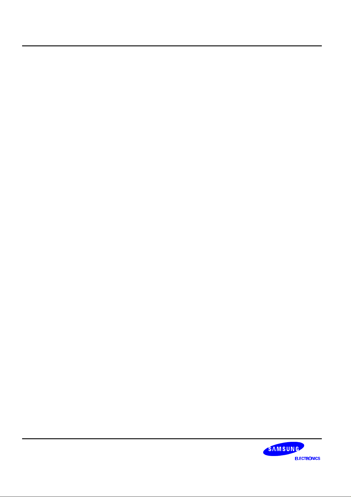
• 80-pin QFP
• Subsystem clock frequency: 32.768 kHz (Typ)
• CPU clock divider circuit (by 4, 8, or 64)
1-3

PRODUCT OVERVIEW KS57C3316/P3316
BLOCK DIAGRAM
P0.0/BTCO
P0.1/TCLO0
P0.2/TCL0
P0.3/BUZ
P1.0/INT0
P1.1/INT1
P1.2/INT2
P1.3/INT4
P2.0
P2.1
P2.2
P2.3
P3.0
P3.1
P3.2
P3.3
P4.0/
SCK
P4.1/SO
P4.2/SI
P4.3/CLO
P5.0/ADC0
P5.1/ADC1
P5.2/ADC2
P5.3/ADC3
I/O Port 0
Input Port 1
I/O Port 2
I/O Port 3
Serial
I/O Port
I/O Port 4
I/O Port 5
A/D
Converter
INT0-INT4
RESET
CE
Interrupt
Control
Block
Internal
Interrupts
Instruction Decoder
Arithmetic
Logic Unit
512 x 4-Bit
Data Memory
XIN
XOUT
and
XTOUT
Clock
XTIN
Program Memory
Basic
Timer
Instruction
Register
Program
Counter
Program
Status Word
Stack
Pointer
16K-Byte
Watch
Timer
Watchdog
Timer
Timer/
Counter 0
IF
Counter
PLL
Synthesizer
LCD Driver/
Controller
Output Port
11,12,13
Output Port
7,8,9,10
I/O Port 6
AMIF
FMIF
VCOAM
VCOFM
EO
BIAS
VLC0-VLC2
COM0-COM3
P13.0-P13.3
/SEG24-SEG27
P12.0-P12.3
/SEG20-SEG23
P11.0-P11.3
/SEG16-SEG19
P10.0-P10.3
/SEG12-SEG15
P9.0-P9.3
/SEG8-SEG11
P8.0-P8.3
/SEG4-SEG7
P7.0-P7.3
/SEG0-SEG3
P6.0-P6.3
KS0-KS3
1-4
Figure 1-1. KS57C3316 Simplified Block Diagram
KS57C3316/P3316 (Preliminary Spec) PRODUCT OVERVIEW
PIN ASSIGNMENTS
P0.1/TCLO0
P0.0/BTCO
P0.2/TCL0
P1.0/INT0
P1.1/INT1
P1.2/INT2
P1.3/INT4
P4.0/
P0.3/BUZ
P4.1/SO
P4.2/SI
P4.3/CLO
P5.0/ADC0
P5.1/ADC1
P5.2/ADC2
P5.3/ADC3
P6.0/KS0
P6.1/KS1
P6.2/KS2
P6.3/KS3
VDD0
VSS0
OUT
X
X
TEST
XT
OUT
XT
RESET
BIAS
VLC0
VLC1
VLC2
COM0
CE
67
38
E0
66
39
VDD1
65
40
64
63
62
61
60
59
58
57
56
55
54
53
52
51
50
49
48
47
46
45
44
43
42
41
FMIF
AMIF
VSS1
VCOAM
VCOFM
P2.3
P2.2
P2.1
P2.0
SEG27/P13.3
SEG26/P13.2
SEG25/P13.1
SEG24/P13.0
SEG23/P12.3
SEG22/P12.2
SEG21/P12.1
SEG20/P12.0
SEG19/P11.3
SEG18/P11.2
SEG17/P11.1
SEG16/P11.0
SEG15/P10.3
SEG14/P10.2
SEG13/P10.1
P3.0
P3.1
P3.2
73
32
72
33
P3.3
70
71
35
34
69
36
68
37
SCK
74
75
76
77
78
79
80
1
2
3
4
5
6
7
8
9
10
11
12
13
14
IN
IN
15
16
17
18
19
20
21
22
23
24
25
26
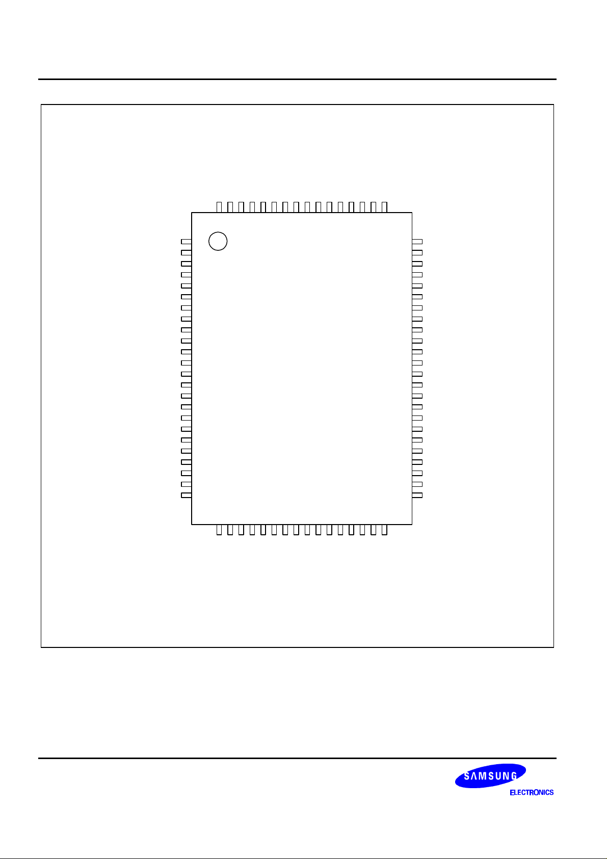
KS57C3316
(80-QFP-Top View)
31
30
29
28
27
SEG12/P10.0
SEG11/P9.3
SEG10/P9.2
SEG9/P9.1
SEG8/P9.0
SEG7/P8.3
SEG6/P8.2
SEG5/P8.1
SEG4/P8.0
SEG3/P7.3
SEG2/P7.2
SEG1/P7.1
SEG0/P7.0
COM3
COM2
COM1
Figure 1-2. KS57C3316 80-QFP Pin Assignment
1-5
PRODUCT OVERVIEW KS57C3316/P3316
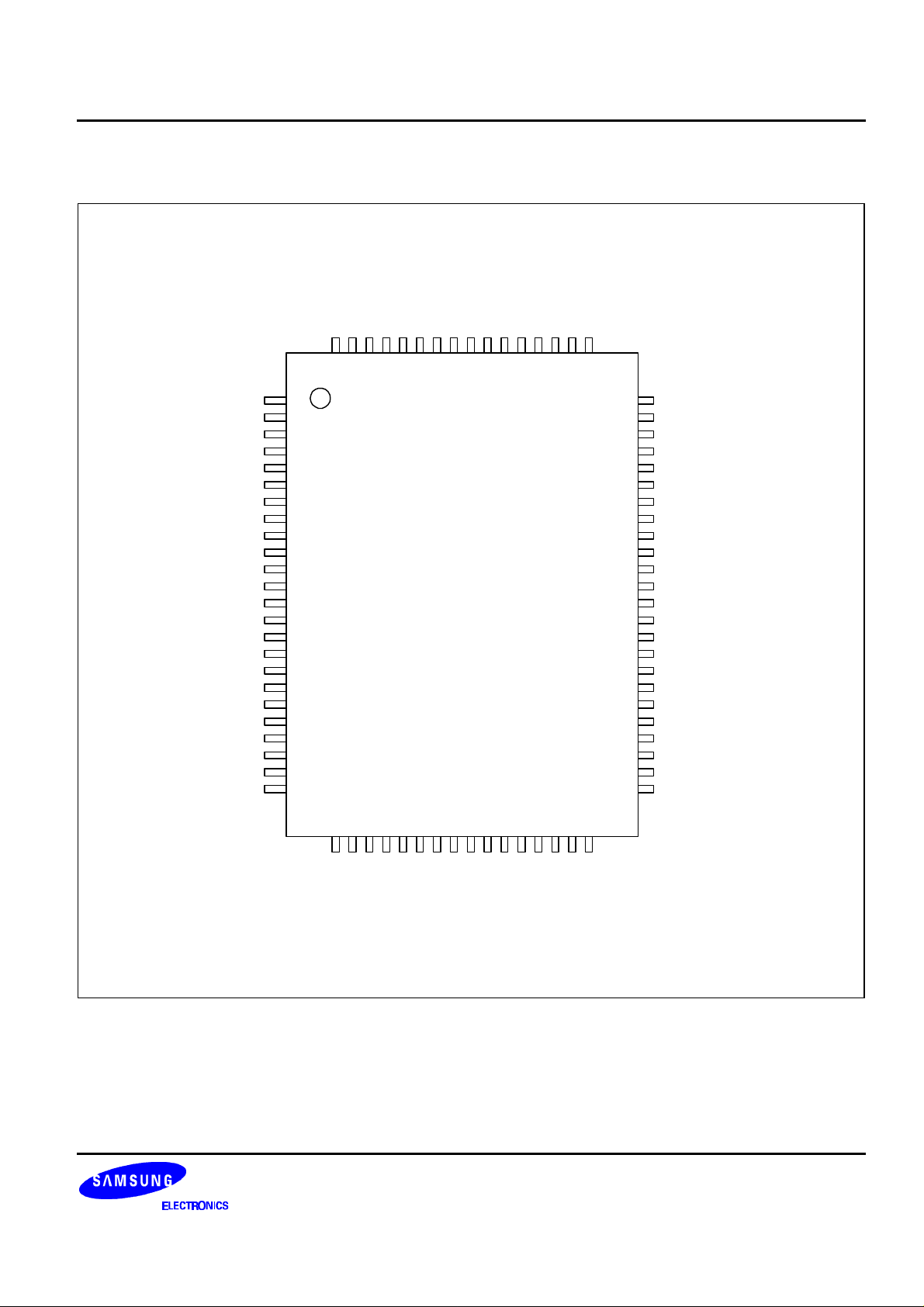
PIN DESCRIPTIONS
Table 1-1. KS57C3316 Pin Descriptions
Pin Name Pin
Type
P0.0
P0.1
P0.2
P0.3
P1.0
P1.1
P1.2
P1.3
P2.0-P2.3
P3.0-P3.3
P4.0
P4.1
P4.2
P4.3
P5.0
P5.1
P5.2
P5.3
P6.0
P6.1
P6.2
P6.3
P7.0
P7.1
P7.2
P7.3
P8.0
P8.1
P8.2
P8.3
P9.0
P9.1
P9.2
P9.3
P10.0
P10.1
P10.2
P10.3
Description Number Share
I/O 4-bit I/O port.
1-bit or 4-bit read, write, and test are possible.
Pull-up resistors can be configured by software.
I 4-bit input port.
1-bit or 4-bit read and test are possible.
Pull-up resistors can be configured by software.
I/O 4-bit I/O ports.
1-bit, 4-bit or 8-bit read, write and test are possible.
Pull-up resistors can be configured by software.
Ports 2 and 3 can be paired to support 8-bit data
transfer.
I/O 4-bit I/O ports.
1-bit, 4-bit or 8-bit read, write and test are possible.
Pull-up resistors can be configured by software.
I/O Ports 4 and 5 can be paired to support 8-bit data
transfer.
I/O 4-bit I/O port.
1-bit, 4-bit or 8-bit read, write and test are possible.
Pull-up resistors can be configured by software.
O 1-bit or 4-bit output port.
Alternatively used for LCD segment output.
O 1-bit or 4-bit output port.
Alternatively used for LCD segment output.
O 1-bit or 4-bit output port.
Alternatively used for LCD segment output.
O 1-bit or 4-bit output port.
Alternatively used for LCD segment output.
72
73
74
75
76
77
78
79
56-59
68-71
80
1
2
3
4
5
6
7
8
9
10
11
28
29
30
31
32
33
34
35
36
37
38
39
40
41
42
43
Reset
Pin
BTCO
Value
Input D-2
TCLO0
TCL0
BUZ
INT0
Input A-4
INT1
INT2
INT4
– Input D-2
SCK
Input D-4
SO
SI
CLO
ADC0
Input F-10
ADC1
ADC2
ADC3
KS0
Input D-7
KS1
KS2
KS3
SEG0
Output H-28
SEG1
SEG2
SEG3
SEG4
Output H-28
SEG5
SEG6
SEG7
SEG8
Output H-28
SEG9
SEG10
SEG11
SEG12
Output H-28
SEG13
SEG14
SEG15
Circuit
Type
D-2
D-4
D-2
D-2
D-4
D-2
1-6
KS57C3316/P3316 (Preliminary Spec) PRODUCT OVERVIEW
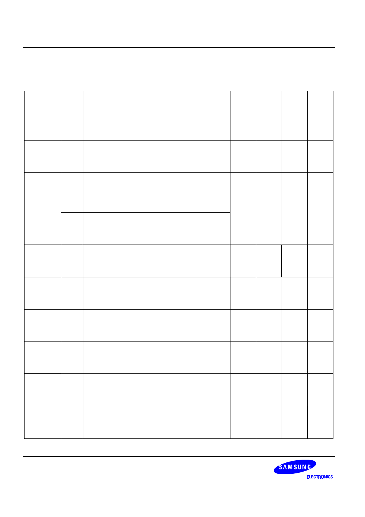
Table 1-1. KS57C3316 Pin Descriptions (Continued)
Pin Name Pin
Type
P11.0
P11.1
P11.2
P11.3
P12.0
P12.1
P12.2
P12.3
P13.0
P13.1
P13.2
P13.3
COM0-
O 1-bit or 4-bit output port.
Alternatively used for LCD segment output.
O 1-bit or 4-bit output port.
Alternatively used for LCD segment output.
O 1-bit or 4-bit output port.
Alternatively used for LCD segment output.
O Common signal output for LCD display 24-27 – Output H
Description Number Share
Pin
44
45
46
47
48
49
50
51
52
53
54
55
SEG16
SEG17
SEG18
SEG19
SEG20
SEG21
SEG22
SEG23
SEG24
SEG25
SEG26
SEG27
Reset
Value
Circuit
Type
Output H-28
Output H-28
Output H-28
COM3
BIAS I LCD power control 20 – Input –
V
LC0
V
LC1
V
LC2
V
DD0
V
SS0
RESET
X
OUT
X
IN
XT
OUT
XT
IN
TEST I
I LCD power supply.
Voltage dividing resistors are assignable by software
21
22
– Input –
23
– Main power supply 12 – – –
– Main Ground 13 – – –
I System reset pin 19 – Input B
– Crystal, or ceramic oscillator pin for main system
clock. (For external clock input, use XIN and input
XIN’s reverse phase to X
OUT
)
– Crystal oscillator pin for subsystem clock. (For
external clock input, use XTIN and input XTIN’s
reverse phase to XT
OUT
)
Test signal input (must be connected to VSS for
14
– – –
15
18
– – –
17
16 – – –
normal operation)
CE I Input pin for checking device power.
67 – Input B-5
Normal operation is high level and PLL/IFC
operation is stopped at low level.
VCOFM
VCOAM
I External VCOFM/AM signal inputs. 60
61
– Input B-4
EO O PLL’s phase error output 66 – Output A-2
FMIF
AMIF
V
DD1
V
SS1
I FM/AM intermediate frequency signal inputs. 64
Input – B-4
63
– PLL/IFC power supply 65 – – –
– PLL/IFC ground 62 – – –
1-7
PRODUCT OVERVIEW KS57C3316/P3316
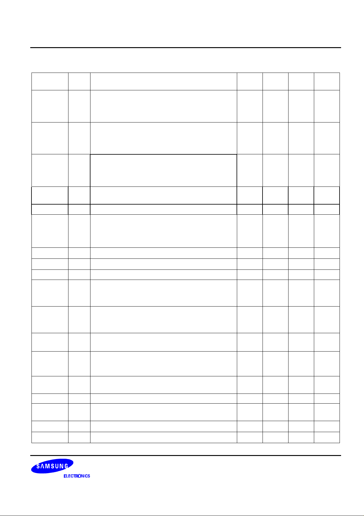
Table 1-1. KS57C3316 Pin Descriptions (Concluded)
Pin Name Pin
Type
Description Number Share
Pin
Reset
Value
Circuit
Type
BTCO I/O Basic timer overflow output signal 72 P0.0 Input D-2
TCLO0 I/O Timer/counter 0 clock output signal 73 P0.1 Input D-2
TCL0 I/O External clock input for timer/counter 0 74 P0.2 Input D-4
BUZ I/O 2,4,8 or 16 kHz frequency output for buzzer sound
75 P0.3 Input D-2
for 4.19 MHz main system clock or 32.768 kHz
subsystem clock
INT0
INT1
I External interrupt. The triggering edges
(rising/falling) are selectable. Only INT0 is
76
77
P1.0
P1.1
Input A-4
synchronized with system clock.
INT2 I Quasi-interrupt with detection of rising edge signal. 78 P1.2
INT4 I External interrupt input with detection of rising or
79 P1.3
falling edges.
SCK
I/O SIO interface clock signal 80 P4.0 Input D-4
SI I/O SIO interface data input signal 1 P4.2
SO I/O SIO interface data output signal 2 P4.1
CLO I/O CPU clock output 3 P4.3
KS0-KS3 I/O Quasi-interrupt input with falling edge detection 8-11 P6.0-
Input D-7
P6.3
ADC0ADC3
SEG0SEG3
SEG4-
I/O ADC input ports. 4-7 P5.0-
Input F-10
P5.3
O LCD segment signal output. 28-31 P7.0-
Output H-28
P7.3
O LCD segment signal output. 32-55 P8-P13 Output H-28
SEG27
1-8
KS57C3316/P3316 (Preliminary Spec) PRODUCT OVERVIEW
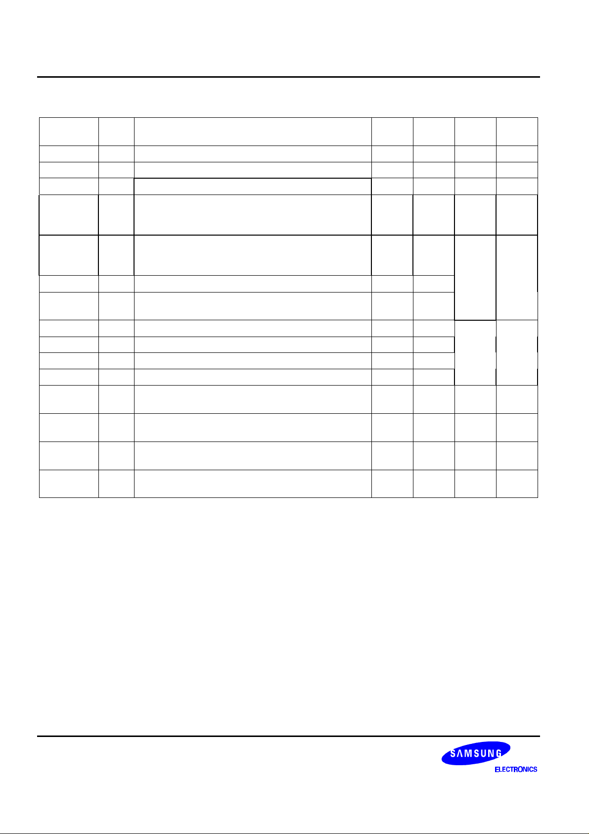
PIN CIRCUIT DIAGRAMS
V
DD
V
DD
P-Channel
In
N-Channel
Figure 1-3. Pin Circuit Type A
V
DD
Up
Down
P-Channel
Out
N-Channel
Pull-Up
Resistor
In
Schmitt Trigger
Figure 1-6. Pin Circuit Type B (RESET)
In
Type A
Feedback
Enable
N-CH
Pull-Down
Enable
Figure 1-4. Pin Circuit Type A-2(EO)
V
DD
Pull-Up
Enable
In
Figure 1-5. Pin Circuit Type A-4 (P1)
Figure 1-7. Pin Circuit Type B-4
In
Figure 1-8. Pin Circuit Type B-5(CE)
1-9
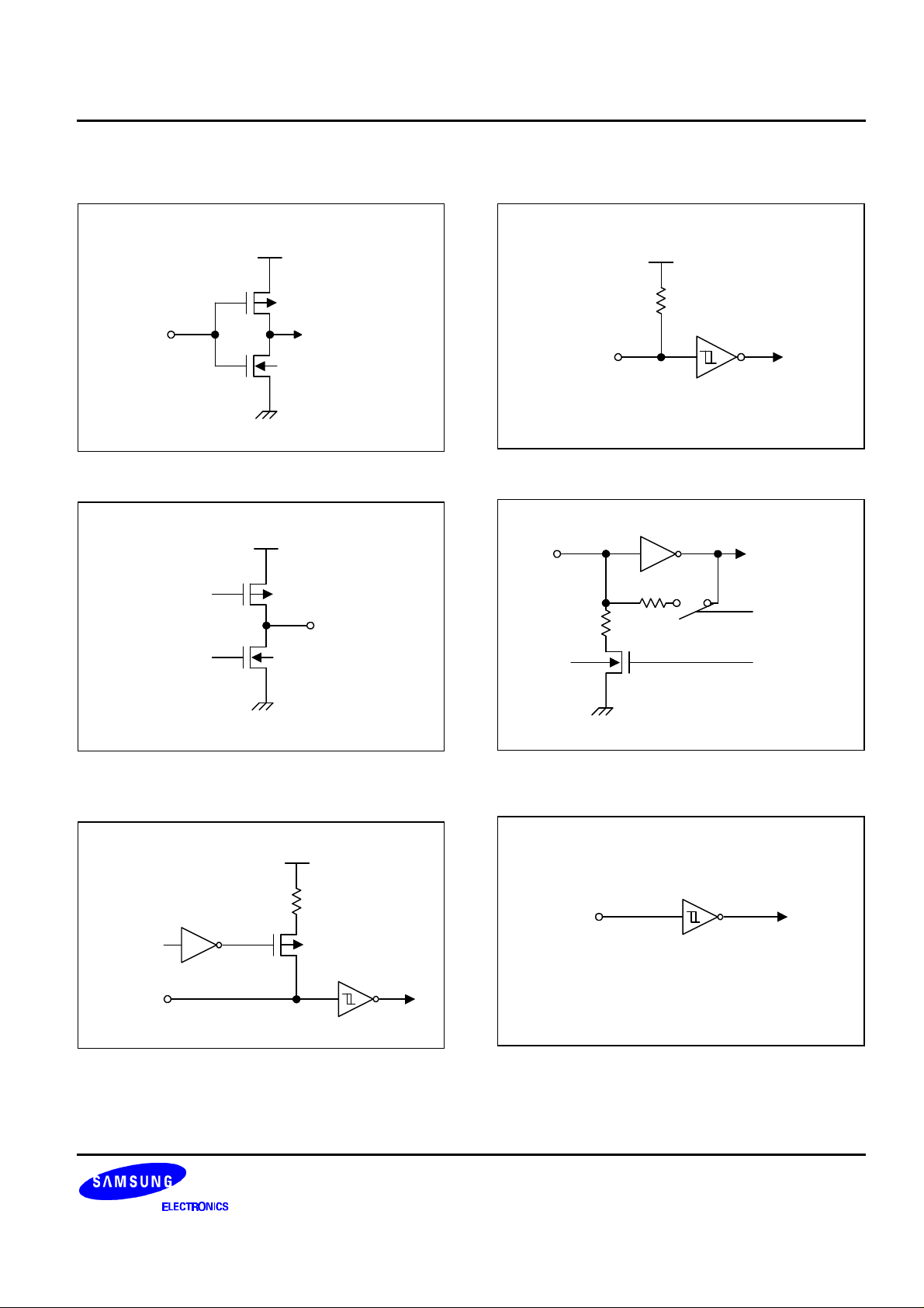
PRODUCT OVERVIEW KS57C3316/P3316
V
DD
V
DD
Data
Output
Disable
P-Channel
Out
N-Channel
Pull-up
Enable
Data
Output
Disable
Circuit
Type C
P-Channel
I/O
Schmitt Trigger
Figure 1-9. Pin Circuit Type C
V
DD
Pull-up
Enable
Data
Output
Circuit
Type C
Disable
Figure 1-10. Pin Circuit Type D-2
P-Channel
I/O
Figure 1-11. Pin Circuit Type D-4
V
DD
Pull-up
Enable
Data
Output
Circuit
Type C
P-Channel
Disable
Enable
Schmitt Trigger
Figure 1-12. Pin Circuit Type D-7 (P6)
I/O
Port
1-10
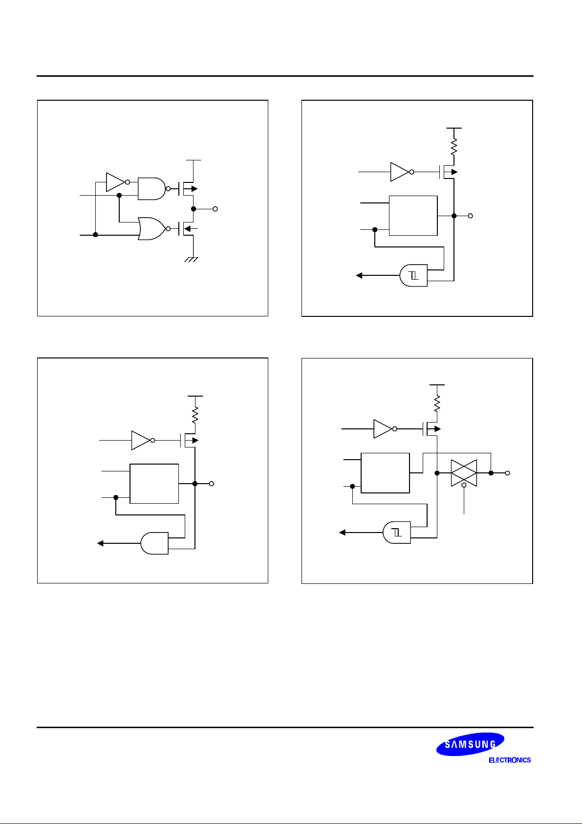
KS57C3316/P3316 (Preliminary Spec) PRODUCT OVERVIEW
V
DD
LC0
V
Pull-up
Enable
LC1
V
Data
Output
Circuit
Type C
Disable
ADCEN
ADC Select
Data
TO ADC
Figure1-13. Pin Circuit Type F-10 (P5)
LC0
V
I/O
SEG
Output
Disable
LC2
V
Figure 1-15. Pin Circuit Type H-4
PNE
Out
DD
V
LC1
V
LCD
COM
LC2
V
Out
Figure 1-14. Pin Circuit Type H (COM0-COM3)
P-CH
Data
N-CH
Output
N-CH
DIsable
Circuit
SEG
Type H-4
Figure 1-16. Pin Circuit Type H-28 (P7-P13)
Output
1-11

KS57C3316/P3316 ELECTRICAL DATA
17 ELECTRICAL DATA
OVERVIEW
In this section, information on KS57C3316 electrical characteristics is presented as tables and graphics. The
information is arranged in the following order:
Standard Electrical Characteristics
— Absolute maximum ratings
— D.C. electrical characteristics
— System clock oscillator characteristics
— I/O capacitance
— A.C. electrical characteristics
— Operating voltage range
Miscellaneous Timing Waveforms
— A.C timing measurement point
— Clock timing measurement at X
— Clock timing measurement at XT
— Input timing for RESET
— Input timing for external interrupts and Quasi-Interrupts
Stop Mode Characteristics and Timing Waveforms
— RAM data retention supply voltage in stop mode
— Stop mode release timing when initiated by RESET
— Stop mode release timing when initiated by an interrupt request
IN
IN
17-1

KS57C3316/P3316 KS57P3316 OTP
18 KS57P3316 OTP
OVERVIEW
The KS57P3316 single-chip CMOS microcontroller is the OTP (One Time Programmable) version of the
KS57C3316 microcontroller. It has an on-chip EPROM instead of masked ROM. The EPROM is accessed by a
serial data format.
The KS57P3316 is fully compatible with the KS57C3316, both in function and in pin configuration. Because of its
simple programming requirements, the KS57P3316 is ideal for use as an evaluation chip for the KS57C3316.
18-1
KS57P3316 OTP KS57C3316/P3316
P0.1/TCLO0
P0.0/BTCO
P0.2/TCL0
P1.0/INT0
P1.1/INT1
P1.2/INT2
P1.3/INT4
P4.0/
P0.3/BUZ
P4.1/SO
P4.2/SI
P4.3/CLO
P5.0/ADC0
P5.1/ADC1
P5.2/ADC2
P5.3/ADC3
P6.0/KS0
P6.1/KS1
SDAT/P6.2/KS2
SCLK/P6.3/KS3
VDD/VDD0
VSS/VSS0
X
OUT
X
VPP/TEST
XT
XT
OUT
RESET
/
RESET
BIAS
VLC0
VLC1
VLC2
COM0
CE
67
38
E0
66
39
VDD1
65
40
64
63
62
61
60
59
58
57
56
55
54
53
52
51
50
49
48
47
46
45
44
43
42
41
FMIF
AMIF
VSS1
VCOAM
VCOFM
P2.3
P2.2
P2.1
P2.0
SEG27/P13.3
SEG26/P13.2
SEG25/P13.1
SEG24/P13.0
SEG23/P12.3
SEG22/P12.2
SEG21/P12.1
SEG20/P12.0
SEG19/11.3
SEG18/P11.2
SEG17/P11.1
SEG16/P11.0
SEG15/P10.3
SEG14/P10.2
SEG13/P10.3
P3.0
P3.1
P3.2
73
72
P3.3
70
71
69
68
SCK
80
79
78
77
76
75
74
1
2
3
4
5
6
7
8
9
10
11
12
13
14
15
IN
KS57P3316
(80-QFP Top View)
16
17
IN
18
19
20
21
22
23
24
37
36
35
34
33
32
31
30
29
28
27
26
25
18-2
SEG12/P10.0
SEG11/P9.3
SEG10/P9.2
SEG9/P9.1
SEG8/P9.0
SEG7/P8.3
SEG6/P8.2
SEG5/P8.1
SEG4/P8.0
SEG3/P7.3
SEG2/P7.2
SEG1/P7.1
SEG0/P7.0
COM3
COM2
COM1
Figure 18-1. KS57P3316 Pin Assignments (80-QFP)

KS57C3316/P3316 KS57P3316 OTP
Table 18-1. Pin Descriptions Used to Read/Write the EPROM
Main Chip During Programming
Pin Name Pin Name Pin No. I/O Function
P6.2 SDAT 10 I/O Serial data pin. Output port when reading and input port
when writing. Can be assigned as a Input or push-pull
output port.
P6.3 SCLK 11 I/O Serial clock pin. Input only pin.
V
TEST
PP
(TEST)
16 I Power supply pin for EPROM cell writing (indicates that
OTP enters into the writing mode). When 12.5 V is
applied, OTP is in writing mode and when 5 V is applied,
OTP is in reading mode.
RESET RESET
V
DD
/ V
SS
VDD / V
SS
19 I Chip initialization
12/13 I
Logic power supply pin. VDD should be tied to +5 V during
programming.
Table 18-2. Comparison of KS57P3316 and KS57C3316 Features
Characteristic KS57P3316 KS57C3316
Program Memory 16K bytes EPROM 16K bytes mask ROM
Operating Voltage (VDD)
OTP Programming Mode
1.8 V to 5.5 V
2.5 V to 3.5 V or 4.0 V to 5.5 V
at PLL/IFC operation
VDD = 5 V, VPP (TEST) = 12.5 V
1.8 V to 5.5 V
2.5 V to 3.5 V or 4.0 V to 5.5 V
at PLL/IFC operation
–
Pin Configuration 80 QFP 80 QFP
EPROM Programmability User Program 1 time Programmed at the factory
OPERATING MODE CHARACTERISTICS
When 12.5 V is supplied to the Vpp (TEST) pin of the KS57P3316, the EPROM programming mode is entered.
The operating mode (read, write, or read protection) is selected according to the input signals to the pins listed in
Table 17-3 below.
Table 18-3. Operating Mode Selection Criteria
V
DD
5 V 5 V 0 0000H 1 EPROM read
Vpp(TEST) REG/MEM Address(A15-A0) R/W Mode
12.5 V 0 0000H 0 EPROM program
12.5 V 0 0000H 1 EPROM verify
12.5 V 1 0E3FH 0 EPROM read protection
NOTE: "0" means low level; "1" means high level.
18-3
KS57P3316 OTP KS57C3316/P3316
Table 18-4. D.C. Electrical Characteristics
(T
= – 40 °C to + 85 °C, VDD = 1.8 V to 5.5 V)
A
Parameter Symbol Conditions Min Typ Max Units
Input high
voltage
Input low
voltage
Output high
voltage
V
V
V
V
V
V
V
IH1
IH2
IH3
IL1
IL2
IL3
OH1
All input pins except those specified
below
P0.2, P1, P4.0, P4.2, P5, P6, CE and
RESET
XIN, X
, XTIN, and XT
OUT
OUT
All input pins except those specified
below
P0.2, P1, P4.0, P4.2, P5, P6, CE and
RESET
XIN, X
, XTIN, and XT
OUT
OUT
VDD = 4.5 V to 5.5 V, EO;
IOH = – 1 mA
0.7 V
0.8 V
DD
DD
–
VDD–0.1 V
– –
0.3 V
0.2 V
VDD–2.0
–
V
V
0.1
V
DD
DD
DD
DD
V
DD
DD
V
OH2
Output low
V
OL1
voltage
V
OL2
Input high
I
LIH
leakage
current
Input low
(note)
I
LIL
leakage
current
Output high
(note)
I
LOH
leakage
current
Output low
(note)
I
LOL
leakage
current
NOTE: Except for XIN, X
(note)
VDD = 4.5 V to 5.5 V;
Other output ports;
IOH = – 1 mA
V
= 4.5 V to 5.5 V, EO;
DD
IOL = 1 mA,
V
= 4.5 V to 5.5 V
DD
Other output ports; IOL = 10 mA
VIN = V
DD
All input pins
V
= 0 V
IN
All input pins
V
= V
OUT
DD
All output pins
V
= 0 V
OUT
All output pins
, XTIN, and XT
OUT
OUT
VDD–1.0 V
– – 2.0
– – 2
– – 3
– – – 3
– – 3
– – – 3
DD
µA
18-4
KS57C3316/P3316 KS57P3316 OTP
Table 18-4. D.C. Electrical Characteristics (Continued)
(T
= – 40 °C to + 85 °C, VDD = 1.8 V to 5.5 V)
A
Parameter Symbol Conditions Min Typ Max Units
V
output
LC0
voltage
V
output
LC1
voltage
V
output
LC2
voltage
COM output
voltage
V
V
V
V
LC0
LC1
LC2
DC
TA = 25 °C
TA = 25 °C
TA = 25 °C
VDD = 5V, (V
LC0
- COM
IO = ± 15 µA (I = 0 - 3)
i I = 0 - 3
0.6 VDD–
0.2
0.4 VDD–
0.2
0.2 VDD–
0.2
)
–
0.6 V
DD
0.6 V
+ 0.2
0.4 V
DD
0.4 V
+ 0.2
0.2 V
DD
0.2 V
+ 0.2
± 45 ± 120
DD
DD
DD
V
mV
deviation
SEG output
voltage
V
DS
VDD = 5V, (V
LC0
- COM
IO = ± 15 µA (I = 0 - 3)
i I = 0 - 3
)
± 45 ± 120
deviation
LCD output
R
LCD
TA = 25 °C
70 100 150
kΩ
voltage
deviation
Oscillator
feed back
resistors
Pull-down
resistor
Pull-up
resistor
R
R
R
R
OSC1
OSC2
R
D
L1
L2
VDD = 5.0 V, TA = 25 °C
XIN = VDD, X
OUT
= 0 V
VDD = 5.0 V, TA = 25 °C
XTIN = VDD, XT
OUT
= 0 V
VDD = 5.0 V, VIN = VDD;
VCOFM, VCOAM, AMIF, and FMIF
V
= 0 V; V
IN
DD
= 5 V
Ports 1, 2, 3, 4, 5, and 6
V
= 3 V
DD
V
= 0 V; V
IN
RESET
V
DD
= 3 V
DD
= 5 V
300 600 1500
1500 3000 4500
15 30 45
25 47 100
50 95 200
100 220 400
200 450 800
18-5
KS57P3316 OTP KS57C3316/P3316
Table 18-4. D.C. Electrical Characteristics (Concluded)
(T
= – 40 °C to + 85 °C, VDD = 1.8 V to 5.5 V)
A
Parameter Symbol Conditions Min Typ Max Units
Supply
Current
(1)
I
DD1
(2)
Main operating:
PCON = 0011B, SCMOD = 0000B
4.5 MHz – 5.5 27 mA
CE = VDD;
Crystal oscillator
C1 = C2 = 22 pF
VDD = 5 V ± 10%
(2)
I
DD2
CE Low mate: 6.0 MHz – 3.5 8
PCON = 0011B, SCMOD = 0000B
4.5 MHz 2.5 5.5
CE = 0 V
Crystal oscillator
C1 = C2 = 22 pF
VDD = 5 V ± 10%
I
DD3
I
DD4
I
DD5
IDD6
I
DD7
V
= 3 V ± 10%
DD
6.0 MHz 1.6 4
4.5 MHz 1.2 3
(2)
Main idle mode: 6.0 MHz – 1.0 2.5
PCON = 0111B, SCMOD =0000B
4.5 MHz 0.9 2.0
Crystal oscillator
C1 = C2 = 22 pF
VDD = 5 V ± 10%
V
= 3 V ± 10%
DD
6.0 MHz 0.5 1.0
4.5MHz 0.4 0.8
(2)
Sub operating mode:
– 15 30 uA
PCON = 0011B, SCMOD = 1001B
CE = 0 V;
V
= 3 V ± 10%
DD
32 kHz crystal oscillator
(2)
Sub idle mode:
– 6 15
PCON = 0111B, SCMOD = 1001B
CE = 0 V;
V
= 3 V ± 10%
DD
32 kHz crystal oscillator
(2)
Stop mode:
– 0.5 3
CPU = fxt/4, SCMOD = 1101B
CE = 0 V;
VDD = 5 V ± 10%
(2)
Stop mode:
–
CPU = fx/4, SCMOD = 0100B
VDD = 5 V ± 10%
NOTES:
1. Supply current does not include current drawn through internal pull-up resistors and LCD voltage dividing resistors.
2. Data includes the power consumption for sub-system clock oscillation.
18-6
 Loading...