


Samsung KS57C21832, KS57P21832 Datasheet

KS57C21832/P21832 PRODUCT OVERVIEW
1-1
1 PRODUCT OVERVIEW
OVERVIEW
The KS57C21832 single-chip CMOS microcontroller has been designed for high performance using Samsung's
newest 4-bit CPU core, SAM47 (Samsung Arrangeable Microcontrollers).
With an up-to-896-dot LCD direct drive capability, 8-bit timer/counter 0, 16-bit timer/counter 1, and serial I/O, the
KS57C21832 offers an excellent design solution for a wide variety of applications which require LCD functions.
Up to 39 pins of the 100-pin QFP package can be dedicated to I/O. Eight vectored interrupts provide fast
response to internal and external events. In addition, the KS57C21832's advanced CMOS technology provides for
low power consumption and a wide operating voltage range.
OTP
The KS57C21832 microcontroller is also available in OTP (One Time Programmable) version, KS57P21832.
KS57P21832 microcontroller has an on-chip 32 K-byte one-time-programable EPROM instead of masked ROM.
The KS57P21832 is comparable to KS57C21832, both in function and in pin configuration.

PRODUCT OVERVIEW KS57C21832/P21832
1-2
FEATURES SUMMARY
Memory
• 8,192 × 4-bit RAM (excluding LCD display RAM)
• 32,768 × 8-bit ROM
39 I/O Pins
• I/O: 35 pins
• Input only: 4 pins
LCD Controller/Driver
• 56 segments and 16 common terminals
• 8 and 16 common selectable
• Internal resistor circuit for LCD bias
• All dot can be switched on/off
8-bit Basic Timer
• 4 interval timer functions
• Watchdog timer
8-bit Timer/Counter 0
• Programmable 8-bit timer
• External event counter
• Arbitrary clock frequency output
• External clock signal divider
• Serial I/O interface clock generator
16-Bit Timer/Counter 1
• Programmable 16-bit timer
• External event counter
• Arbitrary clock frequency output
• External clock signal divider
8-bit Serial I/O Interface
• 8-bit transmit/receive mode
• 8-bit receive mode
• LSB-first or MSB-first transmission selectable
• Internal or external clock source
Memory-Mapped I/O Structure
• Data memory bank 15
Watch Timer
• Time interval generation: 0.5 s, 3.9 ms
at 32768 Hz
• 4 frequency outputs to BUZ pin
• Clock source generation for LCD
Interrupts
• Four internal vectored interrupts
• Four external vectored interrupts
• Two quasi-interrupts
Bit Sequential Carrier
• Supports 16-bit serial data transfer in arbitrary
format
Power-Down Modes
• Idle mode (only CPU clock stops)
• Stop mode (main system clock and CPU clock
stop)
• Sub-system clock stop mode
Oscillation Sources
• Crystal, ceramic, or RC for main system clock
• Crystal oscillator for subsystem clock
• Main system clock frequency: 0.4 - 6 MHz
• Subsystem clock frequency: 32.768 kHz
• CPU clock divider circuit (by 4, 8, or 64)
Instruction Execution Times
• 0.67, 1.33, 10.7 µs at 6 MHz
• 0.95, 1.91, 15.3 µs at 4.19 MHz
• 122 µs at 32.768 kHz
Operating Temperature
• - 40 °C to 85 °C
Operating Voltage Range
• 1.8 V to 5.5 V (3.0 MHz @ 1.8 V)
Package Type
• 100-pin QFP
KS57C21832/P21832 PRODUCT OVERVIEW
1-3
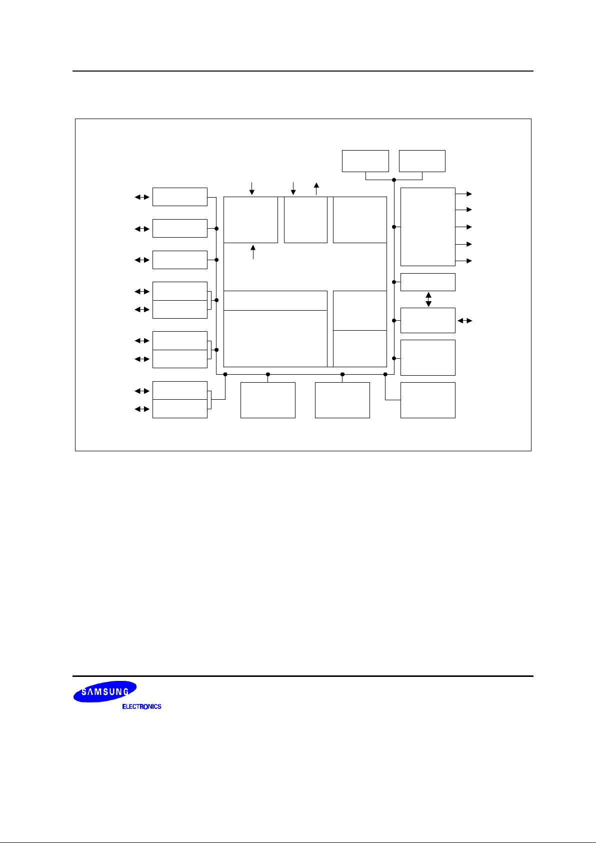
BLOCK DIAGRAM
VLC1-VLC5
COM0-COM7
P4.0-P5.3/
COM8-COM15
SEG0-SEG39
P9.3-P6.0/
SEG40-SEG55
LCD
Driver/
Controller
Program
Status Word
Stack
Pointer
Arithmetic
and
Logic Unit
Instruction
Internal
Interrupts
RESET
P8.0-P8.3
SEG47-SEG44
I/O Port 8
I/O Port 9
P9.0-P9.3
SEG43-SEG40
8-Bit
Timer/
Counter 0
Interrupt
Control
Block
Instruction
Register
Clock
16-Bit
TImer/
Counter 1
32 K Byte
Program
Memory
8192 x 4-Bit
Data
Memory
Serial I/O
I/O
Port 0
P0.0/
SCK
/KO
P0.1/SO/K1
P0.2/SI/K2
P0.3/BUZ/K3
P6.0-P6.3
SEG55-SEG52
KS4-KS7
P7.0-P7.3
SEG51-SEG48
I/O Port 7
I/O Port 6
P5.0-P5.3/
COM12-COM15
P4.0-P4.3/
COM8-COM11
I/O Port 5
I/O Port 4
I/O Port 3
P3.0/TCLO0
P3.1/TCLO1
P3.2/TCL0
P3.3/TCL1
I/O Port 2
P2.0/CLO
P2.1/LCDCK
P2.2/LCDSY
Input Port 1
P1.0-P1.3/
INT0-INT4
XT
OUT
X
OUT
XT
IN
X
IN
Basic
Timer
Watch
Timer
Figure 1-1. KS57C21832 Simplified Block Diagram

PRODUCT OVERVIEW KS57C21832/P21832
1-4
PIN ASSIGNMENTS
SEG5
SEG6
SEG7
SEG8
SEG9
SEG10
SEG11
SEG12
SEG13
SEG14
SEG15
SEG16
SEG17
SEG18
SEG19
SEG20
SEG21
SEG22
SEG23
SEG24
P3.1/TCLO1
P3.2/TCL0
P3.3/TCL1
COM0
COM1
COM2
COM3
COM4
COM5
COM6
COM7
P4.0/COM8
P4.1/COM9
P4.2/COM10
P4.3/COM11
P5.0/COM12
P5.1/COM13
P5.2/COM14
P5.3/COM15
P6.0/SEG55/K4
SEG25
SEG26
SEG27
SEG28
SEG29
SEG30
SEG31
SEG32
SEG33
SEG34
SEG35
SEG36
SEG37
SEG38
SEG39
P9.3/SEG40
P9.2/SEG41
P9.1/SEG42
P9.0/SEG43
P8.3/SEG44
P8.2/SEG45
P8.1/SEG46
P8.0/SEG47
P7.3/SEG48
P7.2/SEG49
P7.1/SEG50
P7.0/SEG51
P6.3/SEG52/K7
P6.2/SEG53/K6
P6.1/SEG54/K5
SEG4
SEG3
SEG2
SEG1
SEG0
VLC5
VLC4
VLC3
VLC2
VLC1
P0.0/
SCK
/K0
P0.1/SO/K1
P0.2/SI/K2
P0.3/BUZ/K3
V
DD
V
SS
X
OUT
X
IN
TEST
XT
IN
XT
OUT
RESET
P1.0/INT0
P1.1/INT1
P1.2/INT2
P1.3/INT4
P2.0/CLO
P2.1/LCDCK
P2.2/LCDSY
P3.0/TCLO0
KS57C21832
(100-QFP-1420C)
1
2
3
4
5
6
7
8
9
10
11
12
13
14
15
16
17
18
19
20
21
22
23
24
25
26
27
28
29
30
80
79
78
77
76
75
74
73
72
71
70
69
68
67
66
65
64
63
62
61
60
59
58
57
56
55
54
53
52
51
31323334353637383940414243444546474849
50
100
99989796959493929190898887868584838281
Figure 1-2. KS57C21832 100-QFP Pin Assignment Diagram

KS57C21832/P21832 PRODUCT OVERVIEW
1-5
PIN DESCRIPTIONS
Table 1-1. KS57C21832 Pin Descriptions
Pin Name Pin Type Description Number Share Pin
P0.0
P0.1
P0.2
P0.3
I/O
4-bit I/O port.
1-bit and 4-bit read/write and test are possible.
Individual pins are software configurable as input or
output.
Individual pins are software configurable as opendrain or push-pull output.
4-bit pull-up resistors are software assignable; pull-up
resistors are automatically disabled for output pins.
11
12
13
14
SCK/K0
SO/K1
SI/K2
BUZ/K3
P1.0
P1.1
P1.2
P1.3
I
4-bit input port.
1-bit and 4-bit read and test are possible.
4-bit pull-up resistors are assignable by software.
23
24
25
26
INT0
INT1
INT2
INT4
P2.0
P2.1
P2.2
I/O Same as port 0 except that port 2 is 3-bit I/O port.
27
28
29
CLO
LCDCK
LCDSY
P3.0
P3.1
P3.2
P3.3
I/O Same as port 0. 30
31
32
33
TCLO0
TCLO1
TCL0
TCL1
P4.0-P4.3
P5.0-P5.3
I/O
4-bit I/O ports.
1-, 4-bit or 8-bit read/write and test are possible.
Individual pins are software configurable as input or
output.
4-bit pull-up resistors are software assignable; pull-up
resistors are automatically disabled for output pins.
42-45
46-49
COM8-
COM11
COM12-
COM15
P6.0-P6.3
P7.0-P7.3
I/O Same as P4, P5.
50-53
54-57
SEG55/K4-
SEG52/K7
SEG51-
SEG48
P8.0-P8.3
P9.0-P9.3
I/O Same as P4, P5. 58-61
62-65
SEG47-
SEG44
SEG43-
SEG40
SCK I/O Serial I/O interface clock signal. 11 P0.0/K0
SO I/O Serial data output. 12 P0.1/K1
SI I/O Serial data input. 13 P0.2/K2
BUZ I/O 2 kHz, 4 kHz, 8 kHz or 16 kHz frequency output for
buzzer signal.
14 P0.3/K3
INT0, INT1 I External interrupts. The triggering edge for INT0 and
INT1 is selectable.
23, 24 P1.0, P1.1

PRODUCT OVERVIEW KS57C21832/P21832
1-6
Table 1-1. KS57C21832 Pin Descriptions (Continued)
Pin Name Pin Type Description Number Share Pin
INT2 I
Quasi-interrupt with detection of rising or falling
edges.
25 P1.2
INT4 I
External interrupt with detection of rising or
falling edges.
26 P1.3
CLO I/O Clock output . 27 P2.0
LCDCK I/O LCD clock output for display expansion. 28 P2.1
LCDSY I/O LCD synchronization clock output for display
expansion.
29 P2.2
TCLO0 I/O Timer/counter 0 clock output. 30 P3.0
TCLO1 I/O Timer/counter 1 clock output. 31 P3.1
TCL0 I/O External clock input for timer/counter 0. 32 P3.2
TCL1 I/O External clock input for timer/counter 1. 33 P3.3
COM0-COM7 O LCD common signal output. 34-41 –
COM8-COM11 I/O 42-45 P4.0-P4.3
COM12-COM15 46-49 P5.0-P5.3
SEG0-SEG39 O LCD segment signal output.
5-1,
100-66
–
SEG40-SEG43 I/O 65-62 P9.3-P9.0
SEG44-SEG47 61-58 P8.3-P8.0
SEG48-SEG51 57-54 P7.3-P7.0
SEG52-SEG55 53-50 P6.3/K7-P6.0/K4
K0-K3 I/O External interrupt. The triggering edge is
selectable.
11-14 P0.0-P0.3
K4-K7 50-53 P6.0-P6.3
V
DD
– Main power supply. 15 –
V
SS
– Ground. 16 –
RESET I Reset signal. 22 –
V
LC1-VLC5
– LCD power supply. 10-6 –
X
in, Xout
– Crystal, Ceramic or RC oscillator pins for
system clock.
18, 17 –
XT
in, XTout
– Crystal oscillator pins for subsystem clock. 20, 21 –
TEST I
Test signal input. (must be connected to VSS)
19 –
NOTE: Pull-up resistors for all I/O ports are automatically disabled if they are configured to output mode.

KS57C21832/P21832 PRODUCT OVERVIEW
1-7
Table 1-2. Overview of KS57C21832 Pin Data
Pin Names Share Pins I/O Type Reset Value Circuit Type
P0.1, P0.3 SO/K1, BUZ/K3 I/O Input E-1
P0.0, P0.2 SCK/K0, SI/K2 I/O Input E-2
P1.0-P1.3 INT0-INT2, INT4 I Input A-3
P2.0-P2.2 CLO, LCDCK, LCDSY I/O Input E
P3.0-P3.1 TCLO0, TCLO1 I/O Input E
P3.2-P3.3 TCL0, TCL1 I/O Input E-1
P4.0-P4.3
P5.0-P5.3
COM8-COM11
COM12-COM15
I/O Input H-13
P6.0-P6.3 SEG55/K4-SEG52/K7
I/O
Input
H-16
P7.0-P7.3 SEG51-SEG48 I/O Input H-13
P8.0-P8.3
P9.0-P9.3
SEG47-SEG44
SEG43-SEG40
I/O
Input
H-13
COM0-COM7 – O High H-3
SEG0-SEG39 – O High H-15
V
DD
– – – –
V
SS
– – – –
RESET – I – B
V
LC1
-
V
LC5
– – – –
X
IN,
X
OUT
– – – –
XT
IN,
XT
OUT
– – – –
TEST – I – –
PRODUCT OVERVIEW KS57C21832/P21832
1-8
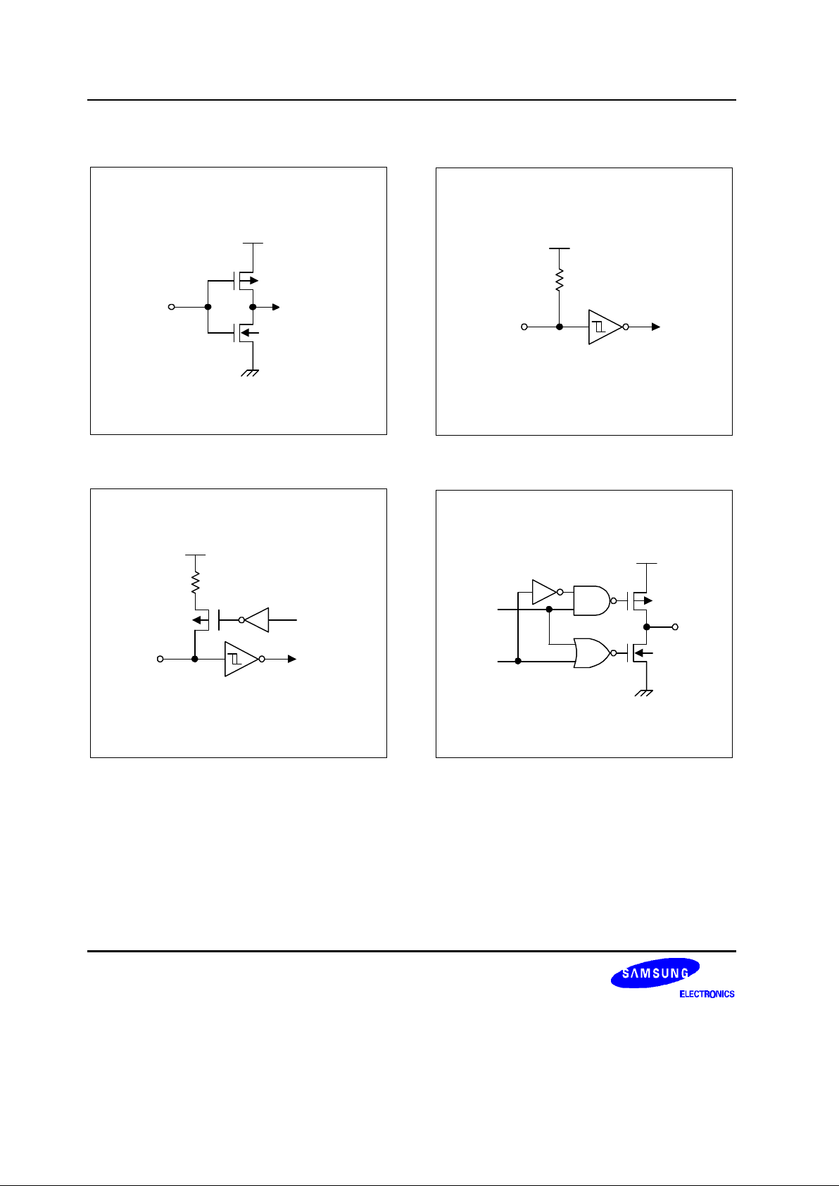
PIN CIRCUIT DIAGRAMS
P-Channel
N-Channel
In
V
DD
Figure 1-3. Pin Circuit Type A
Schmitt Trigger
Pull-Up
Resistor
V
DD
Pull-Up
Resistor
Enable
In
P-Channel
Figure 1-4. Pin Circuit Type A-3
Schmitt Trigger
In
V
DD
Pull-Up
Resistor
Figure 1-5. Pin Circuit Type B
P-Channel
N-Channel
V
DD
Out
Output
DIsable
Data
Figure 1-6. Pin Circuit Type C

KS57C21832/P21832 PRODUCT OVERVIEW
1-9
N-CH
V
DD
Pull-up
Resistor
Enable
V
DD
I/O
PNE
Pull-up
Resistor
P-CH
Output
DIsable
Data
Figure 1-7. Pin Circuit Type E
Schmitt Trigger
N-CH
V
DD
Pull-up
Resistor
Enable
V
DD
I/O
PNE
Pull-up
Resistor
P-CH
Output
DIsable
Data
Figure 1-8. Pin Circuit Type E-1

PRODUCT OVERVIEW KS57C21832/P21832
1-10
N-CH
V
DD
Pull-up
Resistor
Enable
V
DD
I/O
PNE
Pull-up
Resistor
P-CH
Output
DIsable
Data
Schmitt Trigger
Figure 1-9. Pin Circuit Type E-2

KS57C21832/P21832 PRODUCT OVERVIEW
1-11
Out
V
DD
V
LC1
COM
V
LC5
V
LC4
Figure 1-10. Pin Circuit Type H-3
Out
V
DD
V
LC2
SEG
V
LC5
V
LC3
Figure 1-11. Pin Circuit Type H-15