

Samsung KS5520-01, KS5520D-04 Datasheet
JAN. 1998
SPECIFICATION
for KS5520
VID - 97 - D001
SYSTEM LSI BUSINESS
SAMSUNG ELECTRONICS CO.
SPECIFICATION
g
g
g
g
g
g
g
g
g
g
g
g
g
g
g
g
g
g
g
g
for KS5520
CONTENTS
Important Notice
Copyright 1998 by SAMSUNG
The information in this publication has been carefully checked and is believed
to be accurate at the time of publication. Samsun
however, for possible errors or omissions, or for any consequences resultin
from the use of the information contained herein.
reserves the right to make changes in its products or product
Samsun
specifications with the intent to improve function or desi
without notice and is not required to update this documentation to reflect such
es.
chan
This publication does not convey to a purchaser of semiconductor devices
described herein any license under the patent ri
makes no warranty, representation, or guarantee regarding the
Samsun
suitability of its products for any particular purpose, nor does Samsun
assume any liability arising out of the application or use of any product or
circuit and specifically disclaims any liability, includin
consequence or incidental dama
*Typical* parameters can and do vary in different applications. All operatin
parameters, inc luding *Typicals,* must be validated for each customer
application by the customer*s technical experts.
products are not designed, intended, or authorized for use as
Samsun
components in systems intended for sur
applications intended to support or sustain life, or for any other application in
which the failure of the Samsun
death.
Should the buyer purchase or use a Samsun
unintended or unauthorized application, the buyer shall indemnify and hold
and its officers, employees, subsidiaries, affiliates, and distributors
Samsun
harmless a
attorney fees arisin
injury or death that may be associated with such unintended or unauthorized
use, even if such claim alle
desi
ainst all claims, costs, damages, expenses, and reasonable
out of, either directly or indirectly, any claim of personal
n or manufacture or manufacture of said product.
es.
product could cause personal injury or
es that Samsung was negligent regarding the
assumes no responsibility,
n at any time and
hts of Samsung or others.
without limitation any
ical implant into the body, for other
product for any such
OUTLINE OF PRODUCT -------------
•
FUNCTIONS -----------------------------
•
FEATURES -------------------------------
•
OPTION CODE --------------------------
•
ORDERING INFORMATION ---------
•
BLOCK DIAGRAM ---------------------
•
PIN CONFIGURATION ----------------
•
ABSOLUTE MAXIMUM RATING --
•
ELECTRICAL CHARACTERISTICS -
•
TIMING DIAGRAM ----------------------
•
MEMORY STRUCTURE ------- --------
•
SCREEN STRUCTURE ---------------
•
BLANK MODE --------------------------
•
SCROLL/HALF-TONE FUNCTION -
•
BOX DRAWING FUNCTION ---------
•
APPLICATION CIRCUIT --------------
•
PACKAGE DIMENSIONS ------------
•
3
3
3
3
3
4
4
6
7
8
9
15
15
16
17
18
20

KS5520-XX ON SCREEN DISPLAY PROCESSOR
y
g
y
y
y
1. OUTLINE OF PRODUCT
The KS5520 is a single chip VLSI device which performs
the on screen displa
video composite si
It can choose total 256 characters and displa
360 characters in a screen.
It can also select various built-in functions such as
character color select, inverse, etc. These functions are
compatible with all video s
SECAM.
function with sync seperation of
nal and AFC is proposed.
up to
stems including NTSC, PAL,
24 - SDIP - 300
24 - SOP - 375
2. FUNCTIONS
• On screen displa
• Sync separator and sync detector
• AFC
3. FEATURES
á
• Screen structure : 360 ( 30 columns
• Character structure : 12 á 18 dots
• Character types : 256 kinds of color characters
• Display position : 62 horizontal position
64 vertical position
• Character size : 4 á 4 times of normal in both vertical and horizontal directions
• Blinking : controllable in character unit, blinking time also controllable
• Blanking : controllable in line units, blanking mode change possible
Blank color fill possible in character units (8 colors)
• Background coloring : 8 colors
• Character coloring : coloring of characters possible in blank mode
• Inverse character display : controllable in character units
• Synchronous ways : automatic selection of internal or external synchronization via MICOM control
• Built-in clamp, horizontal/vertical sync separator & sync detector circuit
• Sync detection sensitivity can be adjusted via MICOM control.
• Built-in analog horizontal/vertical sync PLL circuit
• Scroll & Box Drawing ability
• Half-Tone function ability
• NTSC / PAL / SECAM mode via MICOM control
12 rows)
4.2 ORDERING INFORMATION
Device Package Operating Temprature
KS5520-XX 24-SDIP-300 - 20 ~ + 70
KS5520D-XX 24-SOP-375 - 20 ~ + 70
4.1 OPTION CODE
Code No.
KS5520-01
KS5520D-04
English, Russian, German, French, Spanish, Italian, Polish, Portuguese, Swedish
Denish, Dutch, Esperanto, Vietnamese, Indonesian, Czechoslovak
English, Russian, German, French, Spanish, Italian, Polish, Portuguese, Swedish
Denish, Dutch, Esperanto, Vietnamese, Indonesian, Czechoslovak, Greek
Remark
VID-97-D001
98-05-14
3

KS5520-XX ON SCREEN DISPLAY PROCESSOR
5. BLOCK DIAGRAM
2
SCK
CSB
SIN
6
7
SERIAL
INTERFACE
HORIZONTAL
CONTROL
TIMING
GENERATOR
ADDRESS
COUNTER
RAM
PARALLEL IN
SERIAL OUT
ROM
MIXER BUFFER
18
19
SCCR
CVOUT
ROM
COLUMN
DECODER
COLOR
SYNC
CONTROL
XTIN
XTOUT
CLAMPIN
VERTICAL
CONTROL
GENERATOR
21
22
9
GENERATOR
GENERATOR
CLAMP
HSYNC
VSYNC
SYNC
SEPARATOR
8
LPF CSYNC SYD
CSYNC
GENERATOR
23 20
6. PIN CONFIGURATION & DESCRIPTION
6.1 PIN CONFIGURATION
DGND
1
CLAMP
SYNC
DELAY
11 12 15 13 14
PD OUT VCO IN R CNTR C N1 C N2
24
LC
OSCILLATOR
PLL
DVDD
17
CVIN
4
OSC IN
OSC OUT
5
SCK
RESETB
OSCIN
OSCOUT
CSB
SIN
LPF
CLAMPIN
AGND
PD OUT
VCO IN
10
11
12
2
3
4
5
6
23
22
21
20
19
CSYNC
XTOUT
XTIN
SYD
CVOUT
KS5520
7
8
9
VID-97-D001
98-05-14
18
17
16
15
14
13
SCCR
CVIN
AVDD
R CNTR
C NOD2
C NOD1
4
KS5520-XX ON SCREEN DISPLAY PROCESSOR
g
y
q
y
g
g
g g
g
g
g
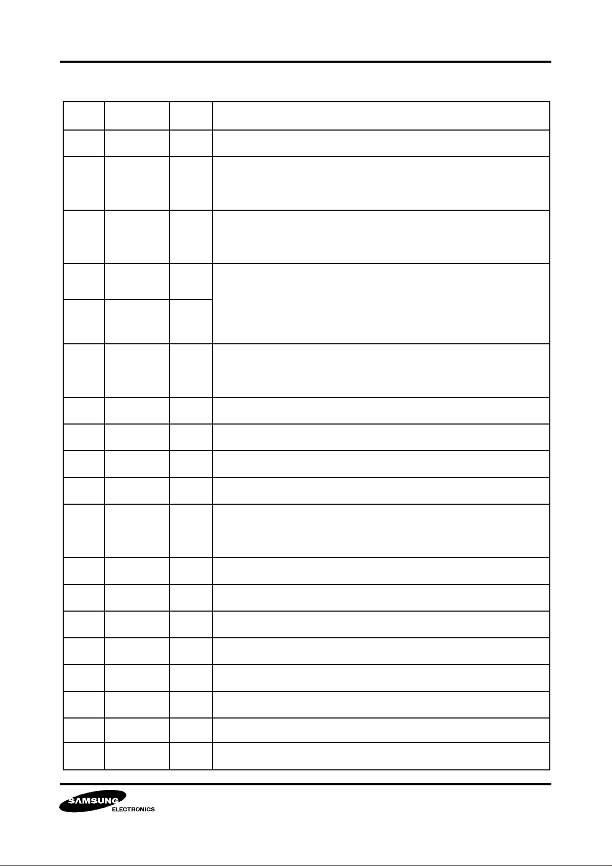
6.2 PIN DESCRIPTION
Pin No. Symbol I/O Function
Di
1
DGND
-
ital Ground
2
3
SCK
RESETB
I
I
Serial clock input. When CSB pin is low, then 16-bit serial
data is inputted b
controlling micom. Built-in pull-up resistor.
Auto clear pin. If low, then all circuit is reset.
Built-in pull-up resistor.
4
OSCIN
I
LC oscillation pin. Standard fre
uency is 9MHz &
the horizontal start position and the horizontal size are controlled
5
6
OSCOUT
CSB
O
the clock of oscillation block.
b
I
While pin 6 is low, serial data input is active.
Built - in pull-up resistor
7
8
9
SIN
LPF
CLAMPIN
I
I
I
Serial data input pin. Built-in pull-up resistor
LPF
ets rid of the color signal in a video input signal.
Clamp input pin of composite video si
nal of 2Vpp
10
11
12
13
14
15
16
17
18
19
AGND
PD OUT
VCO IN
C NOD1
C NOD2
R CNTR
AVDD
CVIN
SCCR
CVOUT
-
O
Analo
Phase detect output of analo
round
PLL. Loop filter is formed by PD
OUT and VCO IN.
I
O
O
O
-
I
I
O
VCO input pin of PLL
Capacitor node 1 of PLL VCO
Capacitor node 2 of PLL VCO
Resistor node of PLL VCO
5V Analo
V
DD
Composite video input pin
When SECAM mode, color si
Composite video output pin
nal is mixed in the character level.
VID-97-D001
98-05-14
5
KS5520-XX ON SCREEN DISPLAY PROCESSOR
(
)
y
y
g
(
)
y
g
6.2 PIN DESCRIPTION
Continued
Pin No. Symbol I/O Function
20
21
22
23
24
SYD
XTIN
XTOUT
CSYNC
DVDD
O
I
O
O
-
H-sync detect output pin. If sync exists, then high if not, low
X-tal input / output pin
NTSC : 14.31818 MHz, PAL : 17.734475MHz
When external, C-s
then internal C-s
DD
5V Di
ital V
nc separator output is out, when internal,
nc is outputted.
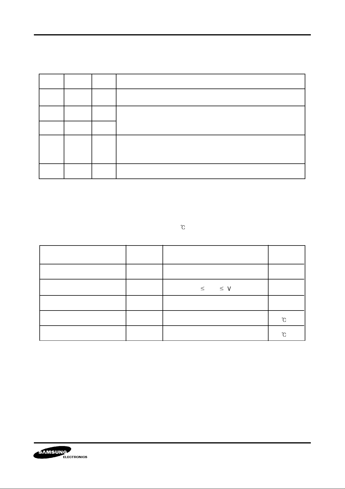
7. ABSOLUTE MAXIMUM RATINGS
Characteristics Symbol Value Unit
Suppl
Voltage
Input Voltage
Power Dissipation
Operating Temperature
Storage Temperature
DD
V
IN
V
D
P
Topr
Tst
Ta = 25
SS
V
3.0 ~ 7.0
þ
- 0.3
- 20 ~ + 70
- 40 ~ + 125
V
IN
200
þ
V
DD
+ 0.3
V
V
mW
VID-97-D001
98-05-14
6
KS5520-XX ON SCREEN DISPLAY PROCESSOR
(
)
g
g
g
g
g
8. ELECTRICAL CHARACTERISTICS
Characteristics Symbol Unit
DD
Operatin
Operatin
Input Hi
Input Low Volta
Output Hi
Voltage
Current
h Voltage
e
h Voltage (2
m
drive)
Output Low Voltage (2m drive)
Pin8 LPF Voltage
Pin9 Clamp Voltage
Pin15 R_CNTR Voltage
Pin17 Clamp Voltage
Buffer Gain
LC Oscillation Frequency
Hsync Duty
V
Icc
IH
V
IL
V
OH
V
OL
V
Vp8
Vp9
Vp15
Vp17
Vp19G
Fosc
Fh_duty
Ta = 25, AV
DD
= DV
Min Typ Max
4.75
20
0.8V
0.7V
2.15
1.25
2.35
0.60
1.80
8.0
250
DD
-
DD
-
5.00
40
-
-
-
-
2.35
1.45
2.50
0.80
2.00
9.0
550
DD
= 5V
5.25
0.2V
0.3V
2.55
1.65
2.65
1.00
2.20
10.0
850
60
V
mA
-
DD
-
DD
V
V
V
V
V
V
V
V
V
MHz
nS
Hsync Frequency
X-tal Oscillation Frequency
Sync Separation Voltage
Blueback Sync Tip Level
Blueback Pedestal Level
Blueback Color Burst Level High
Blueback Color Burst Level Low
Blueback Color Level High
Blueback Color Level Low
Blueback Blank Level High
Blueback Blank Level Low
Blueback Character Level High
Blank Color Off Level
Box White Level
Box Black Level
H_fre
Fp22
Vse
Vbst
Vbpd
Vcbh
Vcbl
Vbch
Vbcl
Vblkh
Vblk1
Vchh
Vbcof
Vbwl
Vbbl
15.5
14.1
0.10
0.50
1.10
1.40
0.80
2.30
1.30
1.40
1.10
2.40
1.10
2.20
1.10
15.7
14.3
0.25
0.80
1.40
1.70
1.10
2.60
1.60
1.70
1.40
2.70
1.40
2.50
1.40
15.9
14.5
0.40
1.10
1.70
2.00
1.40
2.90
1.90
2.00
1.70
3.00
1.70
2.80
1.70
KHz
MHz
V
V
V
V
V
V
V
V
V
V
V
V
V
HalfTone Level
VCO Input Voltage
AFC Freerun Frequency
AFC Lock Range High
AFC Lock Range Low
Note 1 : Specifications are subj ect to change without notice.
Vhalf
Vvco
Ffr
Falh
Fall
VID-97-D001
98-05-14
1.80
2.30
15.5
200
-
2.10
2.50
15.7
300
-
2.40
2.70
15.9
400
-500
V
V
KHz
Hz
Hz
7
 Loading...