

Samsung KS5514B-16, KS5514B-15, KS5514B-12, KS5514B-10, KS5514B-09 Datasheet
...
JAN. 1998
SPECIFICATION
for KS5514B-XX
SYSTEM LSI BUSINESS
SAMSUNG ELECTRONICS CO.

SPECIFICATION
g
g
g
g
g
g
g
g
g
g
g
g
g
g
g
g
g
g
g
g
for KS5514B-XX
CONTENTS
Important Notice
Copyright 1998 by SAMSUNG
The information in this publication has been carefully checked and is believed
to be accurate at the time of publication. Samsun
however, for possible errors or omissions, or for any consequences resultin
from the use of the information contained herein.
reserves the right to make changes in its products or product
Samsun
specifications with the intent to improve function or desi
without notice and is not required to update this documentation to reflect such
es.
chan
This publication does not convey to a purchaser of semiconductor devices
described herein any license under the patent ri
makes no warranty, representation, or guarantee regarding the
Samsun
suitability of its products for any particular purpose, nor does Samsun
assume any liability arising out of the application or use of any product or
circuit and specifically disclaims any liability, includin
consequence or incidental dama
*Typical* parameters can and do vary in different applications. All operatin
parameters, inc luding *Typicals,* must be validated for each customer
application by the customer*s technical experts.
products are not designed, intended, or authorized for use as
Samsun
components in systems intended for sur
applications intended to support or sustain life, or for any other application in
which the failure of the Samsun
death.
Should the buyer purchase or use a Samsun
unintended or unauthorized application, the buyer shall indemnify and hold
and its officers, employees, subsidiaries, affiliates, and distributors
Samsun
harmless a
attorney fees arisin
injury or death that may be associated with such unintended or unauthorized
use, even if such claim alle
desi
ainst all claims, costs, damages, expenses, and reasonable
out of, either directly or indirectly, any claim of personal
n or manufacture or manufacture of said product.
es.
product could cause personal injury or
es that Samsung was negligent regarding the
assumes no responsibility,
n at any time and
hts of Samsung or others.
without limitation any
ical implant into the body, for other
product for any such
FUNCTIONS -------------------------------
•
FEATURES --------------------------------
•
BLOCK DIAGRAM ----------------------
•
PIN DESCRIPTION ----------------------
•
ABSOLUTE MAXIMUM RATINGS --
•
ELECTRICAL CHARACTERISTICS -
•
OPERATION DESCRIPTION ----------
•
TEST CIRCUIT ----------------------------
•
APPLICATION CIRCUIT ---------------
•
PACKAGE DIMENSIONS --------------
•
3
3
3
4
5
6
7
13
14
16

SPECIFICATION
KS5514B -XX ON SCREEN DISPLAY PROCESSOR
ON SCREEN DISPLAY PROCESSOR
The KS5514B is a BICMOS LSI with on screen display
function, sync. separator & expander function.
FUNCTIONS
• On screen display
• Sync separator and sync detector
• General expander
FEATURES
• Character capacity : 240 ( 24 column Ø 10 row )
• Construction of character : 12 Ø 18 dots
• 128 kinds of character
• Display position : 62 horizontal position
: 64 vertical position
• Character si ze : 4 Ø 4 times of normal
• Blinking : character unit
• Background coloring : 8 colors
• Synchronous ways : automatic selection internal
or external synchronization via MICOM control
• General output : 3 ports ( by serial data )
• Built-in sync separator & sync detector
• NTSC / PAL / SECAM mode
• Clamp circuit
BLOCK DIAGRAM
IN
OUT
XT
DVDD P3 P2 SYD AFCR FSC AVDD CVOUT SCC R CVIN
24 23 22 21 20 19 18 17 16 15 14 13
XT
24 - SDIP - 300
ORDERING INFORMATION
Device Package Operating Temprature
KS5514B-XX 24-SDIP-300 - 20 ~ + 70
OPTION CODE INFORMATION
Code No.
- 02
- 03
- 06
- 07
- 09
- 10
- 12
- 13
- 14
- 15
- 16
Remark
English
English, Russian
English
Korean
Korean , English
English, German
English, Arabic
English
Korean , English
English, Chinese
English, Russian, Arabic
Î
DET
SYNC
SEP
SYNC
DETECT
AFC
VIDEO
MIXER
CLAMP
INTERNAL
BIAS CKT
SC
DISPLAY
CONTROL
CONTROL
REGISTER
4F
BLUE BACK
GENERATOR
SHIFT
REGISTER
OSD ROM
OSD RAM
DATA
REGISTER
1 2 3 4 5 6 7 8 9 10 11
DGND SCK ACB OSCIN OSCOUT CSB SIN P1 CLAMPIN AGND LPF AFCF IL
INPUT
CONTROL
ADDR
REGISTER
DISPLAY
OSC
VSYNC
CLAMP
12
398-05-14

SPECIFICATION
KS5514B -XX ON SCREEN DISPLAY PROCESSOR
PIN DESCRIPTION
Pin No. Symbol I/O Function
Digital Ground
1
DGND
-
2
3
4
5
6
7
8
9
SCK
ACB
OSCIN
OSCOUT
CSB
SIN
P1
CLAMPIN
I
Serial clock input. When CSB pin is `L` then serial
data is inp u tted by micom. Hyst er esis inpu t.
I
Auto clear pin. If `L`, then all circuit is reset.
Built-in pull up resistor. Hysteresis input.
I
LC oscillation pin. Standar d freq uency is 7MH z &
the horizontal start position is controlled by the
O
clock of oscillation block.
While pin 6 is low, serial data input is active.
I
Built - in pull up resistor
Serial data input pin. Built-in pull up resistor
I
General output port 1
O
Clamp input pin of composite video signal
I
10
11
12
13
14
15
16
17
18
19
AGND
LPF
AFCFIL
CVIN
SCCR
CVOUT
AVDD
FSC
AFCR
SYD
Analog ground
-
Low pass filter
-
AFC filt er o u tput
-
Composite video signal input
I
SECAM chroma input
I
Composite video output : 2 Vp-p
O
Analog VDD
-
FSC input (Not use)
I
VCO oscillation frequency control
I
When sync signal is inputted, then SYD is high.
O
498-05-14

SPECIFICATION
KS5514B -XX ON SCREEN DISPLAY PROCESSOR
PIN DESCRIPTION
( Continued )
Pin No. Symbol I/O Function
20
21
22
23
24
XT
IN
XT
OUT
P2
P3
DVDD
ABSOLUTE MAXIMUM RATINGS
I
O
O
O
-
X-TAL
X-TAL
General output port 2
General output port 3
Digit al VD D
( Ta = 25Î )
Characteristics Symbol Value Unit
Supp ly Vo ltage
Input Voltage
Power Dissipation
Operating Temperatur e
Storage Temperature
V
DD
V
IN
Pd
Topr
Tstg
V
- 0.3 õ V
SS
- 0.3 ~ 6.0
õ
V
IN
300
- 20 ~ + 70
- 40 ~ + 125
DD
+ 0.3
V
V
mW
Î
Î
598-05-14
SPECIFICATION
KS5514B -XX ON SCREEN DISPLAY PROCESSOR
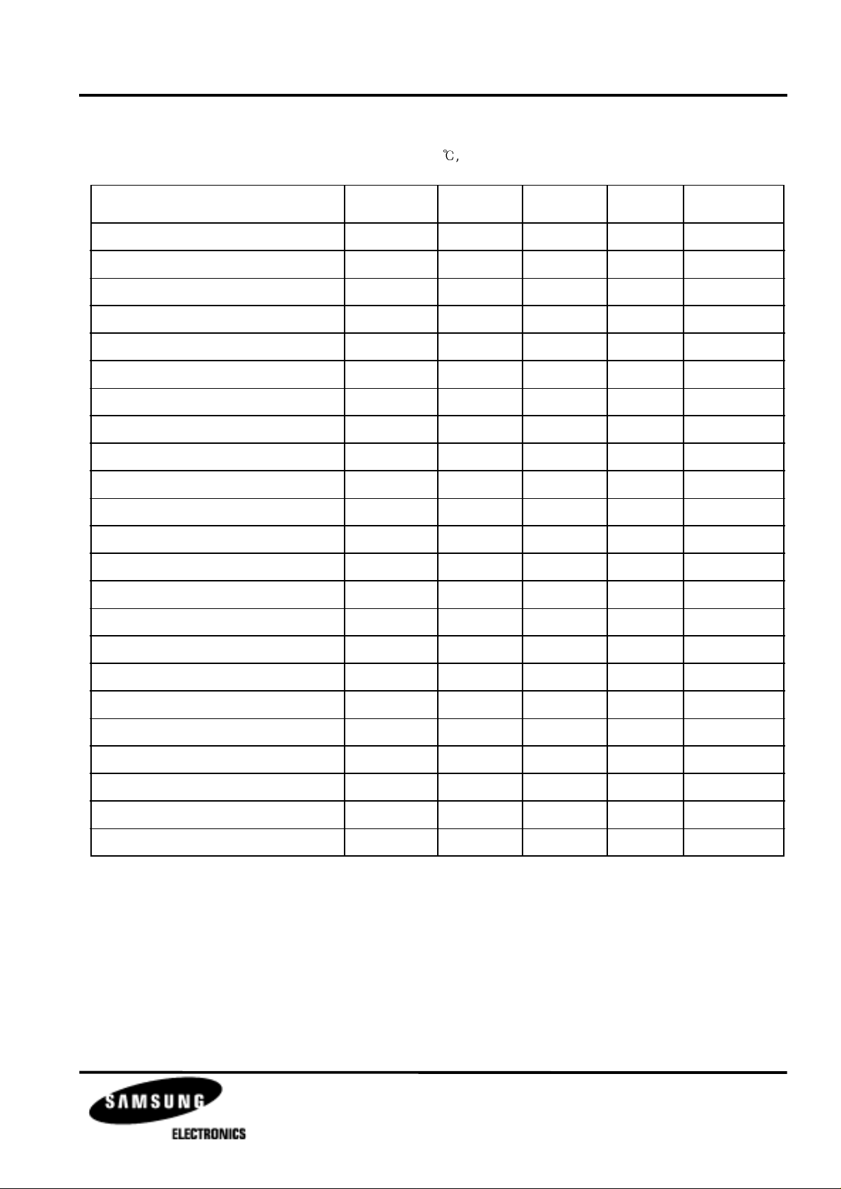
ELECTRICAL CHARACTERISTICS
Characteristics Symbol Unit
Operating Voltage
Operating Voltage
Operating Current
Pin 12 DC Voltage
Pin 13 DC Voltage
AFC Freerun Frequency
AFC Pulse Width
AFC Delay Time
AFC Lock Range H
AFC Lock Rnage L
AFC Capture Range H
AFC Capture Rrange L
DV
AV
Icc
Vpi2
Vpi3
Ffr
twd
td
Falh
Fall
Fach
Fac1
( Ta = 25Î, AV
Min Typ Max
DD
DD
3.5
4.5
10
2.3
1.3
15.5
3.7
1.0
+600
+400
-
DD
= DV
DD
= 5V )
5.0
5.0
20
2.5
1.45
15.7
4.0
2.5
-
-
-
-
5.5
5.5
25
2.7
1.6
15.9
4.3
4.0
-
-900
-
-700
V
V
mA
V
V
KHz
usec
usec
Hz
Hz
Hz
Hz
SYNC DET. Lock Range H
SYNC DET. Lock Range L
SYNC DET. Capture Range H
SYNC DET. Capture Range L
V - SYNC Delay Time
Oscillation Level
Oscillation Frequency
Blueback Sync Tip Level
Blueback Pedestal Level
Blueback Color Burst Level H
Blueb ack Co lor Level H
Flh
Fll
Fch
Fc1
tvd
Vosc
Fosc
Vbst
Vbpd
Vbbh
Vbch
143
6.7
100
14.3
10
4.0
6.3
1.85
2.5
2.75
3.1
153
7.7
107
15.3
14
4.5
7.0
2.05
2.7
2.95
3.3
163
8.7
114
16.3
-
5.0
7.7
2.25
2.9
3.15
3.5
KHz
KHz
KHz
KHz
usec
Vpp
MHz
V
V
V
V
698-05-14
 Loading...