

Samsung KM48S8030DT-G-FL, KM48S8030DT-G-FH, KM48S8030DT-G-FA, KM48S8030DT-G-F8 Datasheet
KM48S8030D
CMOS SDRAM
Rev. 0.0 May 1999
64Mbit SDRAM
Revision 0.0
May 1999
2M x 8Bit x 4 Banks
Synchronous DRAM
LVTTL
* Samsung Electronics reserves the right to change products or specification without notice.
KM48S8030D
CMOS SDRAM
Rev. 0.0 May 1999
Revision History
Revision 0.0 (May 15, 1999)
• Changed tRDL from 1CLK to 2CLK in OPERATING AC PARAMETER.
• Skip ICC4 value of CL=2 in DC characteristics in datasheet.
• Define a new parameter of tDAL( 2CLK +20ns), Last data in to Active delay in OPERATING AC PARAMETER.
• Eliminated FREQUENCY vs.PARAMETER RELATIONSHIP TABLE.
• Symbol Change Notice
Before After
IIL
Input leakage current (inputs)
I
LI
Input leakage current
IIL
Input leakage current (I/O pins)
I
OL
Output open @ DC characteristic table
I
o Output open @ DC characteristic table
• Test Condition in DC CHARACTERISTIC Change Notice
Symbol Before After
I
CC2P , ICC3P
CKE ≤ VIL(max), tCC = 15ns CKE ≤ VIL(max), tCC = 10ns
I
CC2N , ICC3N
CKE ≥ VIH(min), CS ≥ VIH(min), tCC = 15ns
Input signals are changed one time during 30ns
CKE ≥ VIH(min), CS ≥ VIH(min), tCC = 10ns
Input signals are changed one time during 20ns
I
CC4
2 Banks activated 4 Banks activated
KM48S8030D
CMOS SDRAM
Rev. 0.0 May 1999
The KM48S8030D is 67,108,864 bits synchronous high data
rate Dynamic RAM organized as 4 x 2,097,152 words by 8 bits,
fabricated with SAMSUNG′s high performance CMOS technology. Synchronous design allows precise cycle control with the
use of system clock I/O transactions are possible on every clock
cycle. Range of operating frequencies, programmable burst
length and programmable latencies allow the same device to be
useful for a variety of high bandwidth, high performance memory system applications.
• JEDEC standard 3.3V power supply
• LVTTL compatible with multiplexed address
• Four banks operation
• MRS cycle with address key programs
-. CAS latency (2 & 3)
-. Burst length (1, 2, 4, 8 & Full page)
-. Burst type (Sequential & Interleave)
• All inputs are sampled at the positive going edge of the system
clock
• Burst read single-bit write operation
• DQM for masking
• Auto & self refresh
• 64ms refresh period (4K Cycle)
GENERAL DESCRIPTIONFEATURES
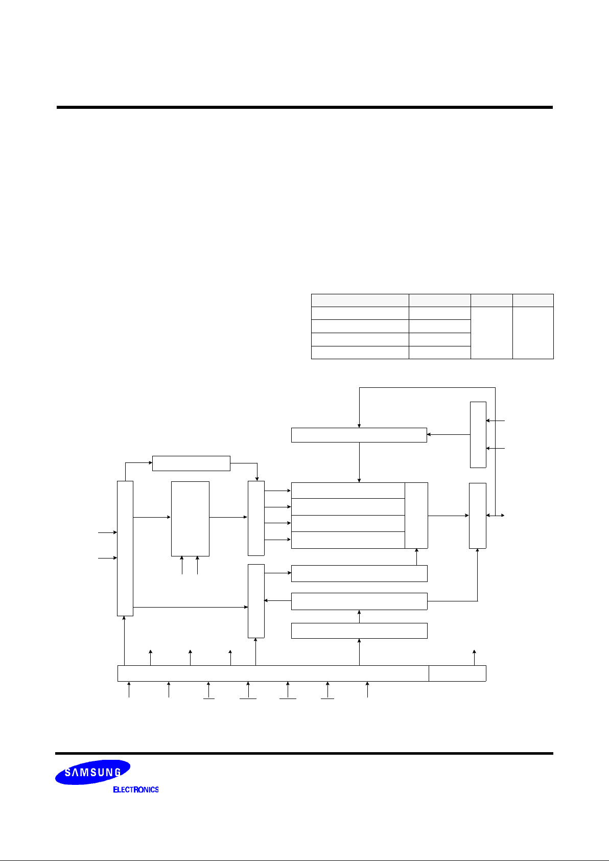
FUNCTIONAL BLOCK DIAGRAM
2M x 8Bit x 4 Banks Synchronous DRAM
Bank Select
Data Input Register
2M x 8
2M x 8
Sense AMP
Output BufferI/O Control
Column Decoder
Latency & Burst Length
Programming Register
Address Register
Row Buffer
Refresh Counter
Row Decoder Col. Buffer
LRAS
LCBR
LCKE
LRAS LCBR LWE LDQM
CLK CKE CS RAS CAS WE DQM
LWE
LDQM
DQi
CLK
ADD
LCAS LWCBR
2M x 8
2M x 8
Timing Register
ORDERING INFORMATION
Part No. Max Freq. Interface Package
KM48S8030DT-G/FA 133MHz(CL=3)
LVTTL
54
TSOP(II)
KM48S8030DT-G/F8 125MHz(CL=3)
KM48S8030DT-G/FH 100MHz(CL=2)
KM48S8030DT-G/FL 100MHz(CL=3)
Samsung Electronics reserves the right to change products or specification without notice.
*
KM48S8030D
CMOS SDRAM
Rev. 0.0 May 1999
VDD
DQ0
VDDQ
N.C
DQ1
VSSQ
N.C
DQ2
VDDQ
N.C
DQ3
VSSQ
N.C
VDD
N.C
WE
CAS
RAS
CS
BA0
BA1
A10/AP
A0
A1
A2
A3
VDD
1
2
3
4
5
6
7
8
9
10
11
12
13
14
15
16
17
18
19
20
21
22
23
24
25
26
27
54
53
52
51
50
49
48
47
46
45
44
43
42
41
40
39
38
37
36
35
34
33
32
31
30
29
28
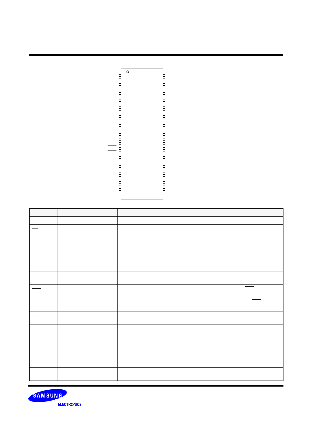
PIN CONFIGURATION
(Top view)
VSS
DQ7
VSSQ
N.C
DQ6
VDDQ
N.C
DQ5
VSSQ
N.C
DQ4
VDDQ
N.C
VSS
N.C/RFU
DQM
CLK
CKE
N.C
A11
A9
A8
A7
A6
A5
A4
VSS
54Pin TSOP (II)
(400mil x 875mil)
(0.8 mm Pin pitch)
PIN FUNCTION DESCRIPTION
Pin Name Input Function
CLK System clock Active on the positive going edge to sample all inputs.
CS Chip select
Disables or enables device operation by masking or enabling all inputs except
CLK, CKE and DQM
CKE Clock enable
Masks system clock to freeze operation from the next clock cycle.
CKE should be enabled at least one cycle prior to new command.
Disable input buffers for power down in standby.
A0 ~ A11 Address
Row/column addresses are multiplexed on the same pins.
Row address : RA0 ~ RA11, Column address : CA0 ~ CA8
BA0 ~ BA1 Bank select address
Selects bank to be activated during row address latch time.
Selects bank for read/write during column address latch time.
RAS Row address strobe
Latches row addresses on the positive going edge of the CLK with RAS low.
Enables row access & precharge.
CAS Column address strobe
Latches column addresses on the positive going edge of the CLK with CAS low.
Enables column access.
WE Write enable
Enables write operation and row precharge.
Latches data in starting from CAS, WE active.
DQM Data input/output mask
Makes data output Hi-Z, tSHZ after the clock and masks the output.
Blocks data input when DQM active.
DQ0 ~ 7 Data input/output Data inputs/outputs are multiplexed on the same pins.
VDD/VSS Power supply/ground Power and ground for the input buffers and the core logic.
VDDQ/VSSQ Data output power/ground
Isolated power supply and ground for the output buffers to provide improved noise
immunity.
N.C/RFU
No connection
/reserved for future use
This pin is recommended to be left No Connection on the device.
 Loading...