

Samsung K9F5608U0A-YIB0, K9F5608U0A-YCB0 Datasheet
K9F5608U0A-YCB0,K9F5608U0A-YIB0
FLASH MEMORY
1
Document Title
32M x 8 Bit NAND Flash Memory
Revision History
The attached datasheets are prepared and approved by SAMSUNG Electronics. SAMSUNG Electronics CO., LTD. reserve the right
to change the specifications. SAMSUNG Electronics will evaluate and reply to your requests and questions about device. If you have
any questions, please contact the SAMSUNG branch office near you.
Revision No.
0.0
0.1
0.2
0.3
0.4
Remark
Advanced
Information
Preliminary
Preliminary
History
Initial issue.
1. Support copy-back program
- The copy-back program is configured to quickly and efficiently rewrite
data stored in one page within the array to another page within the
same array without utilizing an external memory. Since the time-con
suming sequently-reading and its re-loading cycles are removed, the
system performance is improved. The benefit is especially obvious
when a portion of a block is updated so that the rest of the block also
need to be copied to the newly assigned free block.
1. Explain how pointer operation works in detail.
2. For partial page programming into the copied page
- Once the copy-back Program is finished, any additional partial page
programming into the copied pages is prohibited before erase.
3. Renamed GND input (pin # 6) on behalf of SE (pin # 6)
- The SE input controls the access of the spare area. When SE is high,
the spare area is not accessible for reading or programming. SE is rec
ommended to be coupled to GND or Vcc and should not be toggled
during reading or programming.
=> Connect this input pin to GND or set to static low state unless the
sequential read mode excluding spare area is used.
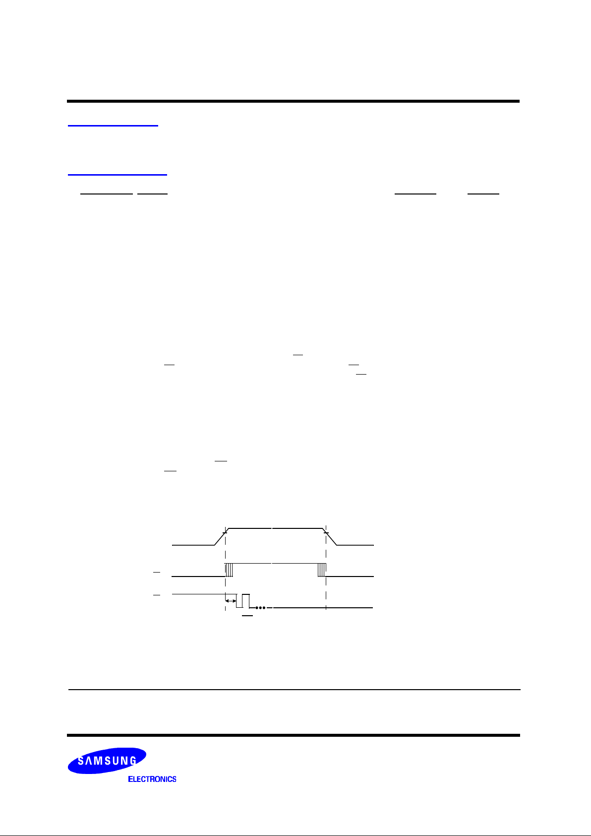
4. Updated operation for tRST timing
- If reset command(FFh) is written at Ready state, the device goes into
Busy for maximum 5us.
1. In addition, explain WE function in pin description
- The WE must be held high when outputs are activated.
1.Powerup sequence is added
: Recovery time of minimum 1µs is required before internal circuit gets
ready for any command sequences
2. AC parameter tCLR(CLE to RE Delay, min 50ns) is added.
3. AC parameter tAR1 value : 100ns --> 20ns
V
CC
WP
High
≈
≈
~ 2.5V
~ 2.5V
≈
WE
1µ
Draft Date
July 17th 2000
Oct. 4th 2000
Nov. 20th 2000
Mar. 2th 2001
Jul. 22th 2001
Note : For more detailed features and specifications including FAQ, please refer to Samsung’s Flash web site.
http://www.intl.samsungsemi.com/Memory/Flash/datasheets.html
K9F5608U0A-YCB0,K9F5608U0A-YIB0
FLASH MEMORY
2
32M x 8 Bit NAND Flash Memory
The K9F5608U0A are a 32M(33,554,432)x8bit NAND Flash
Memory with a spare 1,024K(1,048,576)x8bit. Its NAND cell
provides the most cost-effective solution for the solid state
mass storage market. A program operation programs the 528byte page in typical 200µs and an erase operation can be performed in typical 2ms on a 16K-byte block. Data in the page
can be read out at 50ns cycle time per byte. The I/O pins serve
as the ports for address and data input/output as well as command inputs. The on-chip write controller automates all program and erase functions including pulse repetition, where
required, and internal verification and margining of data. Even
the write-intensive systems can take advantage of the
K9F5608U0A′s extended reliability of 100K program/erase
cycles by providing ECC(Error Correcting Code) with real time
mapping-out algorithm.
The K9F5608U0A-YCB0/YIB0 is an optimum solution for large
nonvolatile storage applications such as solid state file storage
and other portable applications requiring non-volatility.
GENERAL DESCRIPTIONFEATURES
• Voltage Supply : 2.7V~3.6V
• Organization
- Memory Cell Array : (32M + 1024K)bit x 8bit
- Data Register : (512 + 16)bit x8bit
• Automatic Program and Erase
- Page Program : (512 + 16)Byte
- Block Erase : (16K + 512)Byte
• 528-Byte Page Read Operation
- Random Access : 10µs(Max.)
- Serial Page Access : 50ns(Min.)
• Fast Write Cycle Time
- Program time : 200µs(Typ.)
- Block Erase Time : 2ms(Typ.)
• Command/Address/Data Multiplexed I/O Port
• Hardware Data Protection
- Program/Erase Lockout During Power Transitions
• Reliable CMOS Floating-Gate Technology
- Endurance : 100K Program/Erase Cycles
- Data Retention : 10 Years
• Command Register Operation
• Intelligent Copy-Back
• Package :
- K9F5608U0A-YCB0/YIB0 :
48 - Pin TSOP I (12 x 20 / 0.5 mm pitch)
PIN CONFIGURATION
NOTE : Connect all VCC and VSS pins of each device to common power supply outputs.
Do not leave VCC or VSS disconnected.
K9F5608U0A-YCB0/YIB0
1
2
3
4
5
6
7
8
9
10
11
12
13
14
15
16
17
18
19
20
21
22
23
24
48
47
46
45
44
43
42
41
40
39
38
37
36
35
34
33
32
31
30
29
28
27
26
25
N.C
N.C
N.C
N.C
N.C
GND
R/B
RE
CE
N.C
N.C
Vcc
Vss
N.C
N.C
CLE
ALE
WE
WP
N.C
N.C
N.C
N.C
N.C
N.C
N.C
N.C
N.C
I/O7
I/O6
I/O5
I/O4
N.C
N.C
N.C
Vcc
Vss
N.C
N.C
N.C
I/O3
I/O2
I/O1
I/O0
N.C
N.C
N.C
N.C
Pin Name Pin Function
I/O0 ~ I/O7 Data Input/Outputs
CLE Command Latch Enable
ALE Address Latch Enable
CE Chip Enable
RE Read Enable
WE Write Enable
WP Write Protect
GND GND input for enabling spare area
R/B Ready/Busy output
VCC Power
VSS Ground
N.C No Connection
PIN DESCRIPTION
K9F5608U0A-YCB0,K9F5608U0A-YIB0
FLASH MEMORY
3
512Byte 16 Byte
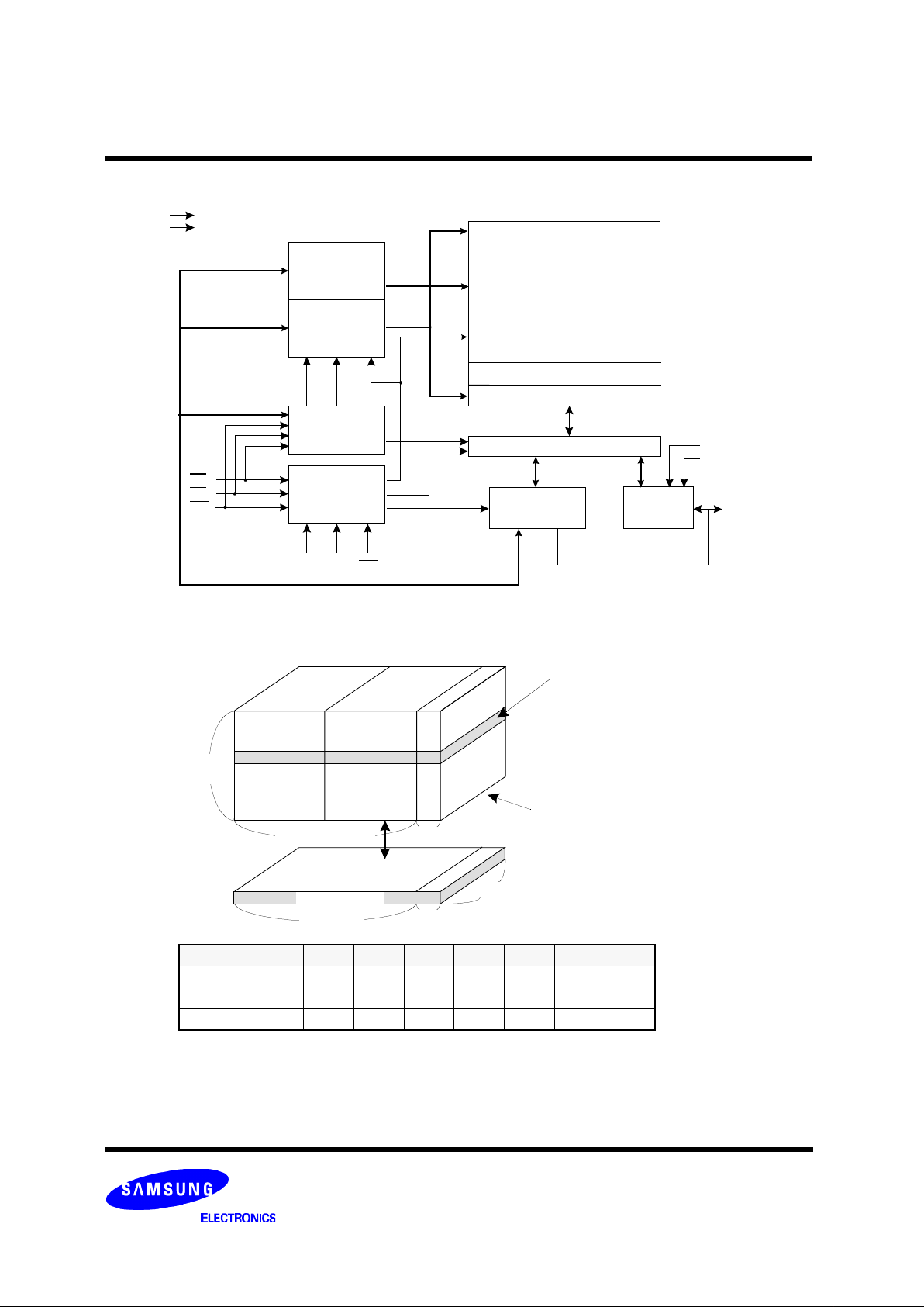
Figure 1. FUNCTIONAL BLOCK DIAGRAM
Figure 2. ARRAY ORGANIZATION
NOTE : Column Address : Starting Address of the Register.
00h Command(Read) : Defines the starting address of the 1st half of the register.
01h Command(Read) : Defines the starting address of the 2nd half of the register.
* A8 is set to "Low" or "High" by the 00h or 01h Command.
* The device ignores any additional input of address cycles than reguired.
I/O 0 I/O 1 I/O 2 I/O 3 I/O 4 I/O 5 I/O 6 I/O 7
1st Cycle A0 A1 A2 A3 A4 A5 A6 A7
2nd Cycle A9 A10 A11 A12 A13 A14 A15 A16
3rd Cycle A17 A18 A19 A20 A21 A22 A23 A24
VCC
X-Buffers
256M + 8M Bit
Command
NAND Flash
ARRAY
(512 + 16)Byte x 65536
Y-Gating
Page Register & S/A
I/O Buffers & Latches
Latches
& Decoders
Y-Buffers
Latches
& Decoders
Register
Control Logic
& High Voltage
Generator
Global Buffers
Output
Driver
VSS
A9 - A24
A0 - A7
Command
CE
RE
WE
WP
I/0 0
I/0 7
VCC
VSS
A8
1st half Page Register
(=256 Bytes)
2nd half Page Register
(=256 Bytes)
64K Pages
(=2,048 Blocks)
512 Byte
8 bit
16 Byte
1 Block =32 Pages
= (16K + 512) Byte
I/O 0 ~ I/O 7
1 Page = 528 Byte
1 Block = 528 Byte x 32 Pages
= (16K + 512) Byte
1 Device = 528Bytes x 32Pages x 2048 Blocks
= 264 Mbits
Column Address
Row Address
(Page Address)
Page Register
CLE ALE
K9F5608U0A-YCB0,K9F5608U0A-YIB0
FLASH MEMORY
4
PRODUCT INTRODUCTION
The K9F5608U0A is a 264Mbit(276,824,064 bit) memory organized as 65,536 rows(pages) by 528 columns. Spare sixteen columns
are located from column address of 512 to 527. A 528-byte data register is connected to memory cell arrays accommodating data
transfer between the I/O buffers and memory during page read and page program operations. The memory array is made up of 16
cells that are serially connected to form a NAND structure. Each of the 16 cells resides in a different page. A block consists of the 32
pages formed by two NAND structures, totaling 8448 NAND structures of 16 cells. The array organization is shown in Figure 2. The
program and read operations are executed on a page basis, while the erase operation is executed on a block basis. The memory
array consists of 2048 separately erasable 16K-byte blocks. It indicates that the bit by bit erase operation is prohibited on the
K9F5608U0A.
The K9F5608U0A has addresses multiplexed into 8 I/O′s. This scheme dramatically reduces pin counts and allows systems upgrades
to future densities by maintaining consistency in system board design. Command, address and data are all written through I/O′s by
bringing WE to low while CE is low. Data is latched on the rising edge of WE. Command Latch Enable(CLE) and Address Latch
Enable(ALE) are used to multiplex command and address respectively, via the I/O pins. All commands require one bus cycle except
for Block Erase command which requires two cycles: one cycle for erase-setup and another for erase-execution after block address
loading. The 32M byte physical space requires 25 addresses, thereby requiring three cycles for byte-level addressing: column
address, low row address and high row address, in that order. Page Read and Page Program need the same three address cycles following the required command input. In Block Erase operation, however, only the two row address cycles are used. Device operations
are selected by writing specific commands into the command register. Table 1 defines the specific commands of the K9F5608U0A.
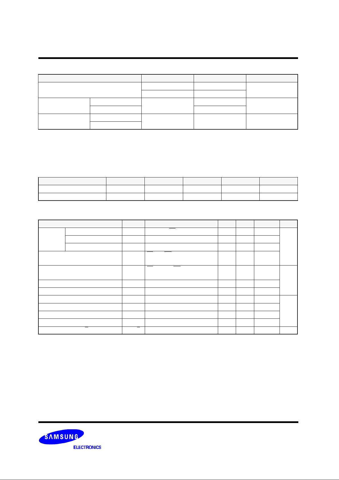
Table 1. COMMAND SETS
NOTE : 1. The 00h command defines starting address of the 1st half of registers.
The 01h command defines starting address of the 2nd half of registers.
After data access on the 2nd half of register by the 01h command, the status pointer is
automatically moved to the 1st half register(00h) on the next cycle.
2. The 50h command is valid only when the GND input(pin # 6) is low level.
Function 1st. Cycle 2nd. Cycle Acceptable Command during Busy
Read 1
00h/01h
(1)
-
Read 2
50h
(2)
Read ID 90h Reset FFh - O
Page Program 80h 10h
Copy-Back Program 00h 8Ah
Block Erase 60h D0h
Read Status 70h - O
Caution : Any undefined command inputs are prohibited except for above command set of Table 1.

K9F5608U0A-YCB0,K9F5608U0A-YIB0
FLASH MEMORY
5
PIN DESCRIPTION
Command Latch Enable(CLE)
The CLE input controls the activating path for commands sent to the command register. When active high, commands are latched
into the command register through the I/O ports on the rising edge of the WE signal.
Address Latch Enable(ALE)
The ALE input controls the activating path for address to the internal address registers. Addresses are latched on the rising edge of
WE with ALE high.
Chip Enable(CE)
The CE input is the device selection control. When CE goes high during a read operation the device is returned to standby mode.
However, when the device is in the Busy state during program or erase, CE high is ignored, and does not return the device to
standby mode.
Write Enable(WE)
The WE input controls writes to the I/O port. Commands, address and data are latched on the rising edge of the WE pulse.
The WE must be held high when outputs are activated.
Read Enable(RE)
The RE input is the serial data-out control, and when active drives the data onto the I/O bus. Data is valid tREA after the falling edge
of RE which also increments the internal column address counter by one.
GND (Pin # 6)
Connect this input pin to GND or set to static low state unless the sequential read mode excluding spare area is used.
I/O Port : I/O 0 ~ I/O 7
The I/O pins are used to input command, address and data, and to output data during read operations. The I/O pins float to high-z
when the chip is deselected or when the outputs are disabled.
Write Protect(WP)
The WP pin provides inadvertent write/erase protection during power transitions. The internal high voltage generator is reset when
the WP pin is active low.
Ready/Busy(R/B)
The R/B output indicates the status of the device operation. When low, it indicates that a program, erase or random read operation is
in process and returns to high state upon completion. It is an open drain output and does not float to high-z condition when the chip
is deselected or when outputs are disabled.
K9F5608U0A-YCB0,K9F5608U0A-YIB0
FLASH MEMORY
6
DC AND OPERATING CHARACTERISTICS(Recommended operating conditions otherwise noted.)
Parameter Symbol Test Conditions Min Typ Max Unit
Operating
Current
Sequential Read ICC1 tRC=50ns, CE=VIL, IOUT=0mA - 10 20
mA
Program ICC2 - - 10 20
Erase ICC3 - - 10 20
Stand-by Current(TTL) ISB1
CE=VIH, WP=GND input (Pin #6)
= 0V/VCC
- - 1
Stand-by Current(CMOS) ISB2
CE=VCC-0.2, WP=GND input (Pin
#6) = 0V/VCC
- 10 50
µA
Input Leakage Current ILI VIN=0 to 3.6V - - ±10
Output Leakage Current ILO VOUT=0 to 3.6V - - ±10
Input High Voltage VIH - 2.0 - VCC+0.3
V
Input Low Voltage, All inputs VIL - -0.3 - 0.8
Output High Voltage Level VOH IOH=-400µA 2.4 - Output Low Voltage Level VOL IOL=2.1mA - - 0.4
Output Low Current(R/B) IOL(R/B) VOL=0.4V 8 10 - mA
RECOMMENDED OPERATING CONDITIONS
(Voltage reference to GND, K9F5608U0A-YCB0 :TA=0 to 70°C, K9F5608U0A-YIB0:TA=-40 to 85°C)
Parameter Symbol Min Typ. Max Unit
Supply Voltage VCC 2.7 3.3 3.6 V
Supply Voltage VSS 0 0 0 V
ABSOLUTE MAXIMUM RATINGS
NOTE :
1. Minimum DC voltage is -0.6V on input/output pins. During transitions, this level may undershoot to -2.0V for periods <30ns.
Maximum DC voltage on input/output pins is VCC,+0.3V which, during transitions, may overshoot to VCC+2.0V for periods <20ns.
2. Permanent device damage may occur if ABSOLUTE MAXIMUM RATINGS are exceeded. Functional operation should be restricted to the conditions
as detailed in the operational sections of this data sheet. Exposure to absolute maximum rating conditions for extended periods may affect reliability.
Parameter Symbol Rating Unit
Voltage on any pin relative to VSS
VIN -0.6 to + 4.6
V
VCC -0.6 to + 4.6
Temperature Under Bias
K9F5608U0A-YCB0
TBIAS
-10 to +125
°C
K9F5608U0A-YIB0 -40 to +125
Storage Temperature
K9F5608U0A-YCB0
TSTG -65 to +150 °C
K9F5608U0A-YIB0
K9F5608U0A-YCB0,K9F5608U0A-YIB0
FLASH MEMORY
7
CAPACITANCE(TA=25°C, VCC=3.3V, f=1.0MHz)
NOTE : Capacitance is periodically sampled and not 100% tested.
Item Symbol Test Condition Min Max Unit
Input/Output Capacitance CI/O VIL=0V - 10 pF
Input Capacitance CIN VIN=0V - 10 pF
VALID BLOCK
NOTE :
1. The K9F5608U0A may include invalid blocks when first shipped. Additional invalid blocks may develop while being used. The number of valid blocks
is presented with both cases of invalid blocks considered. Invalid blocks are defined as blocks that contain one or more bad bits. Do not erase or
program factory-marked bad blocks. Refer to the attached technical notes for a appropriate management of invalid blocks.
2. The 1st block, which is placed on 00h block address, is fully guaranteed to be a valid block, does not require Error Correction.
Parameter Symbol Min Typ. Max Unit
Valid Block Number NVB 2013 - 2048 Blocks
Program/Erase Characteristics
Parameter Symbol Min Typ Max Unit
Program Time tPROG - 200 500 µs
Number of Partial Program Cycles
in the Same Page
Main Array
Nop
- - 2 cycles
Spare Array - - 3 cycles
Block Erase Time tBERS - 2 3 ms
AC TEST CONDITION
(K9F5608U0A-YCB0 :TA=0 to 70°C, K9F5608U0A-YIB0:TA=-40 to 85°C, VCC=2.7V~3.6V unless otherwise)
Parameter Value
Input Pulse Levels 0.4V to 2.4V
Input Rise and Fall Times
5ns
Input and Output Timing Levels 1.5V
Output Load (3.0V +/-10%) 1 TTL GATE and CL=50pF
Output Load (3.3V +/-10%) 1 TTL GATE and CL=100pF
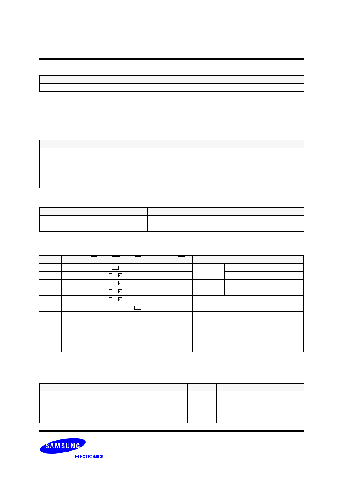
MODE SELECTION
NOTE : 1. X can be VIL or VIH.
2. WP should be biased to CMOS high or CMOS low for standby.
3. When GND input is high, spare area is deselected.
CLE ALE CE WE RE GND WP Mode
H L L H X X
Read Mode
Command Input
L H L H X X Address Input(3clock)
H L L H X H
Write Mode
Command Input
L H L H X H Address Input(3clock)
L L L H
L/H
(3)
H Data Input
L L L H
L/H
(3)
X Sequential Read & Data Output
L L L H H
L/H
(3)
X During Read(Busy)
X X X X X
L/H
(3)
H During Program(Busy)
X X X X X X H During Erase(Busy)
X
X
(1)
X X X X L Write Protect
X X H X X
0V/VCC
(2)
0V/VCC
(2)
Stand-by
K9F5608U0A-YCB0,K9F5608U0A-YIB0
FLASH MEMORY
8
AC Characteristics for Operation
NOTE :
1. The time to Ready depends on the value of the pull-up resistor tied R/B pin.
2. To break the sequential read cycle, CE must be held high for longer time than tCEH.
3. If reset command(FFh) is written at Ready state, the device goes into Busy for maximum 5us.
Parameter Symbol Min Max Unit
Data Transfer from Cell to Register tR - 10 µs
ALE to RE Delay( ID read ) tAR1 20 - ns
ALE to RE Delay(Read cycle) tAR2 50 - ns
CLE to RE Delay tCLR 50 - ns
Ready to RE Low tRR 20 - ns
RE Pulse Width tRP 30 - ns
WE High to Busy tWB - 100
ns
Read Cycle Time tRC 50 - ns
RE Access Time tREA - 35 ns
RE High to Output Hi-Z tRHZ 15 30 ns
CE High to Output Hi-Z
tCHZ - 20 ns
RE High Hold Time tREH 15 - ns
Output Hi-Z to RE Low tIR 0 - ns
Last RE High to Busy(at sequential read) tRB - 100 ns
CE High to Ready(in case of interception by CE at read)
tCRY
-
50 +tr(R/B)
(1)
ns
CE High Hold Time(at the last serial read)
(2)
tCEH 100 - ns
CE Low to Status Output tCEA - 45 ns
WE High to RE Low tWHR 60 - ns
RE access time(Read ID) tREADID - 35 ns
Device Resetting Time(Read/Program/Erase) tRST -
5/10/500
(3)
µs
AC Timing Characteristics for Command / Address / Data Input
NOTE : 1. If tCS is set less than 10ns, tWP must be minimum 35ns, otherwise, tWP may be minimum 25ns.
Parameter Symbol Min Max Unit
CLE Set-up Time tCLS 0 - ns
CLE Hold Time tCLH 10 - ns
CE Setup Time tCS 0 - ns
CE Hold Time
tCH 10 - ns
WE Pulse Width tWP
25
(1)
- ns
ALE Setup Time tALS 0 - ns
ALE Hold Time
tALH 10 -
ns
Data Setup Time tDS 20 - ns
Data Hold Time tDH 10 - ns
Write Cycle Time tWC 50 - ns
WE High Hold Time
tWH 15 - ns
K9F5608U0A-YCB0,K9F5608U0A-YIB0
FLASH MEMORY
9
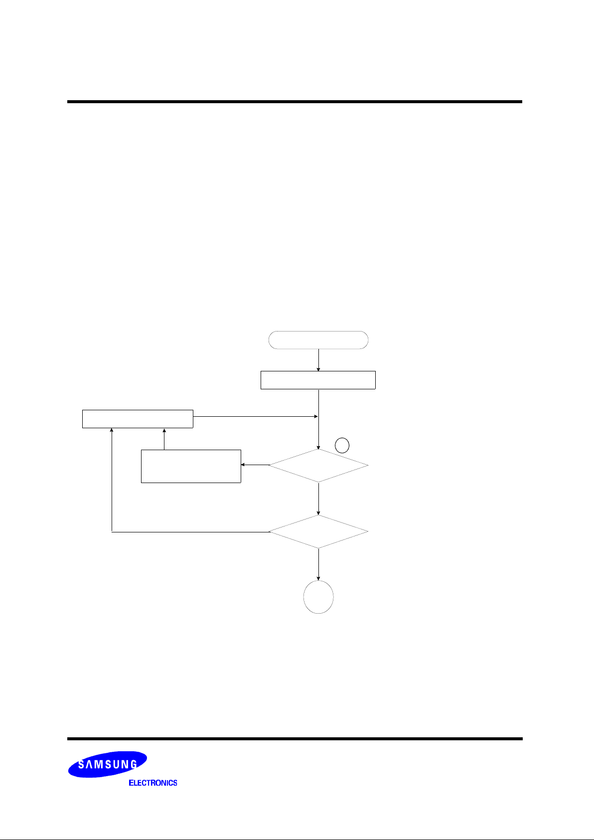
NAND Flash Technical Notes
Identifying Invalid Block(s)
Invalid Block(s)
Invalid blocks are defined as blocks that contain one or more invalid bits whose reliability is not guaranteed by Samsung. The information regarding the invalid block(s) is so called as the invalid block information. Devices with invalid block(s) have the same quality
level or as devices with all valid blocks and have the same AC and DC characteristics. An invalid block(s) does not affect the performance of valid block(s) because it is isolated from the bit line and the common source line by a select transistor. The system design
must be able to mask out the invalid block(s) via address mapping. The 1st block, which is placed on 00h block address, is fully guaranteed to be a valid block, does not require Error Correction.
All device locations are erased(FFh) except locations where the invalid block(s) information is written prior to shipping. The invalid
block(s) status is defined by the 6th byte in the spare area. Samsung makes sure that either the 1st or 2nd page of every invalid
block has non-FFh data at the column address of 517. Since the invalid block information is also erasable in most cases, it is impossible to recover the information once it has been erased. Therefore, the system must be able to recognize the invalid block(s) based
on the original invalid block information and create the invalid block table via the following suggested flow chart(Figure 1). Any intentional erasure of the original invalid block information is prohibited.
*
Check "FFh" at the column address 517
Figure 1. Flow chart to create invalid block table.
Start
Set Block Address = 0
Check "FFh" ?
Increment Block Address
Last Block ?
End
No
Yes
Yes
Create (or update)
No
Invalid Block(s) Table
of the 1st and 2nd page in the block
 Loading...