

SAMSUNG K9F1G08U0A Technical data
现货库存、技术资料、百科信息、热点资讯,精彩尽在鼎好!
K9F1G08R0A
K9F1G08U0A
K9K2G08U1A FLASH MEMORY
Document Title
128M x 8 Bit / 256M x 8 Bit NAND Flash Memory
Revision History
Revision No
0.0
0.1
0.2
0.3
0.4
0.5
0.6
0.7
History
1. Initial issue
1. The tADL(Address to Data Loading Time) is added.
- tADL Minimum 100ns (Page 11, 23~26)
-
tADL is the time from the WE rising edge of final address cycle
to the WE
2. Added Addressing method for program operation
1. Add the Protrusion/Burr value in WSOP1 PKG Diagram.
1. PKG(TSOP1, WSOP1) Dimension Change
1. Technical note is changed
2. Notes of AC timing characteristics are added
3. The description of Copy-back program is changed
4. Voltage range is changed
-1.7V~1.95V -> 1.65V~1.95V
5. Note2 of Command Sets is added
1. CE
1. The value of tREA for 3.3V device is changed.(18ns->20ns)
2. EDO mode is added.
1. The flow chart to creat the initial invalid block table is cahnged.
rising edge of first data cycle at program operation.
access time : 23ns->35ns (p.11)
Draft Date
Aug. 24. 2003
Jan. 27. 2004
Apr. 23. 2004
May. 19. 2004
Jan. 21. 2005
Feb. 14. 2005
May. 24. 2005
May 6. 2005
Remark
Advance
Preliminary
Preliminary
Preliminary
Preliminary
Preliminary
The attached data sheets are prepared and approved by SAMSUNG Electronics. SAMSUNG Electronics CO., LTD. reserve the right
to change the specifications. SAMSUNG Electronics will evaluate and reply to your requests and questions about device. If you have
any questions, please contact the SAMSUNG branch office near your office.
1
K9F1G08R0A
K9F1G08U0A
K9K2G08U1A FLASH MEMORY
128M x 8 Bit /256M x 8 Bit NAND Flash Memory
PRODUCT LIST
Part Number Vcc Range Organization PKG Type
K9F1G08R0A 1.65 ~ 1.95V
K9F1G08U0A-Y,P
K9F1G08U0A-V,F WSOP1
K9K2G08U1A-I 52-ULGA
2.7 ~ 3.6V
FEATURES
• Voltage Supply
-1.8V device(K9F1G08R0A): 1.65V~1.95V
-3.3V device(K9F1G08U0A): 2.7 V ~3.6 V
• Organization
- Memory Cell Array : (128M + 4,096K)bit x 8bit
- Data Register : (2K + 64)bit x8bit
- Cache Register : (2K + 64)bit x8bit
• Automatic Program and Erase
- Page Program : (2K + 64)Byte
- Block Erase : (128K + 4K)Byte
• Page Read Operation
- Page Size : 2K-Byte
- Random Read : 25µs(Max.)
- Serial Access : 30ns(Min.) - 3.3v device
50ns(Min.) -1.8v device
• Fast Write Cycle Time
- Program time : 200µs(Typ.)
- Block Erase Time : 2ms(Typ.)
• Command/Address/Data Multiplexed I/O Port
• Hardware Data Protection
- Program/Erase Lockout During Power Transitions
• Reliable CMOS Floating-Gate Technology
- Endurance : 100K Program/Erase Cycles
- Data Retention : 10 Years
• Command Register Operation
• Cache Program Operation for High Performance Program
• Intelligent Copy-Back Operation
• Unique ID for Copyright Protection
• Package :
- K9F1G08U0A-YCB0/YIB0
48 - Pin TSOP I (12 x 20 / 0.5 mm pitch)
- K9F1G08U0A-VIB0
48 - Pin WSOP I (12X17X0.7mm)
- K9F1G08U0A-PCB0/PIB0
48 - Pin TSOP I (12 x 20 / 0.5 mm pitch)- Pb-free Package
- K9F1G08U0A-FIB0
48 - Pin WSOP I (12X17X0.7mm)- Pb-free Package
* K9F1G08U0A-V,F(WSOPI ) is the same device as
K9F1G08U0A-Y,P(TSOP1) except package type.
- K9K2G08U1A-ICB0/IIB0
52-ULGA (12X17X0.65mm)
X8
Only available in MCP
TSOP1
GENERAL DESCRIPTION
Offered in 128Mx8bit the K9F1G08X0A is 1G bit with spare 32M bit capacity. Its NAND cell provides the most cost-effective solution
for the solid state mass storage market. A program operation can be performed in typical 200µs on the 2112-byte page and an erase
operation can be performed in typical 2ms on a 128K-byte block. Data in the data page can be read out at 30ns(50ns with 1.8V
device) cycle time per byte. The I/O pins serve as the ports for address and data input/output as well as command input. The on-chip
write controller automates all program and erase functions including pulse repetition, where required, and internal verification and
margining of data. Even the write-intensive systems can take advantage of the K9F1G08X0A′s extended reliability of 100K program/
erase cycles by providing ECC(Error Correcting Code) with real time mapping-out algorithm. The K9F1G08X0A is an optimum solution for large nonvolatile storage applications such as solid state file storage and other portable applications requiring non-v ol at il it y.
2
K9F1G08R0A
K9F1G08U0A
PIN CONFIGURATION (TSOP1)
PACKAGE DIMENSIONS
48-PIN LEAD/LEAD FREE PLASTIC THIN SMALL OUT-LINE PACKAGE TYPE(I)
K9K2G08U1A FLASH MEMORY
K9F1G08X0A-YCB0,PCB0/YIB0,PIB0
X8 X8
N.C
N.C
N.C
N.C
N.C
N.C
N.C
R/B
RE
CE
N.C
N.C
Vcc
Vss
N.C
N.C
CLE
ALE
WE
WP
N.C
N.C
N.C
N.C
N.C
1
2
3
4
5
6
7
8
9
10
11
12
13
14
15
16
17
18
19
20
21
22
23
24
48-pin TSOP1
Standard Type
12mm x 20mm
48
N.C
47
N.C
46
N.C
45
I/O7
44
I/O6
43
I/O5
42
I/O4
41
N.C
40
N.C
39
N.C
38
Vcc
37
Vss
36
N.C
35
N.C
34
N.C
33
I/O3
32
I/O2
31
I/O1
30
I/O0
29
N.C
28
N.C
27
N.C
26
N.C
25
48 - TSOP1 - 1220AF
+0.07
-0.03
#1
0.20
+0.003
-0.001
+0.07
-0.03
0.16
0.008
0.50
0.0197
#24
TYP
0.25
0.010
0~8°
20.00±0.20
0.787±0.008
18.40±0.10
0.724±0.004
#48
#25
Unit :mm/Inch
MAX
0.10
0.004
0.25
0.010
()
MAX
12.00
0.472
0.488
12.40
1.00±0.05
0.039±0.002
1.20
MAX
+0.075
0.035
+0.003
-0.001
0.125
0.005
0.047
0.05
0.002
MIN
0.45~0.75
0.018~0.030
0.50
()
0.020
3
K9F1G08R0A
K9F1G08U0A
PIN CONFIGURATION (WSOP1)
PACKAGE DIMENSIONS
48-PIN LEAD PLASTIC VERY VERY THIN SMALL OUT-LINE PACKAGE TYPE (I)
K9K2G08U1A FLASH MEMORY
K9F1G08U0A-VIB0,FIB0
N.C
N.C
DNU
N.C
N.C
N.C
R/B
RE
CE
DNU
N.C
Vcc
Vss
N.C
DNU
CLE
ALE
WE
WP
N.C
N.C
DNU
N.C
N.C
1
2
3
4
5
6
7
8
9
10
11
12
13
14
15
16
17
18
19
20
21
22
23
24
48
47
46
45
44
43
42
41
40
39
38
37
36
35
34
33
32
31
30
29
28
27
26
25
N.C
N.C
DNU
N.C
I/O7
I/O6
I/O5
I/O4
N.C
DNU
N.C
Vcc
Vss
N.C
DNU
N.C
I/O3
I/O2
I/O1
I/O0
N.C
DNU
N.C
N.C
48 - WSOP1 - 1217F
#1
+0.07
-0.03
0.16
+0.07
-0.03
0.20
0.50TYP
(0.50±0.06)
#24
15.40±0.10
#48
#25
0.70 MAX
0.58±0.04
(0.01Min)
Unit :mm
12.00±0.10
12.40MAX
17.00±0.20
+0.075
-0.035
0.10
0
°
~
8
°
0.45~0.75
4
K9F1G08R0A
K9F1G08U0A
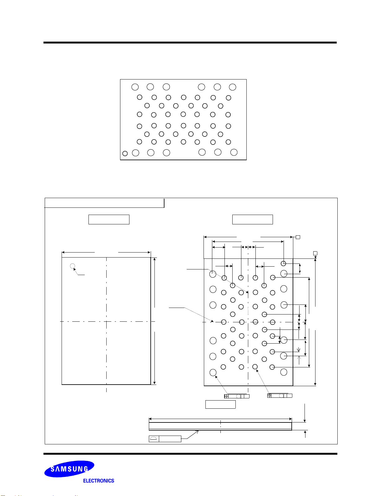
PIN CONFIGURATION (ULGA)
K9K2G08U1A FLASH MEMORY
K9K2G08U1A-ICB0/IIB0
AB
CDE
G
F
L
M
K
H
J
N
7
6
5
4
3
2
1
PACKAGE DIMENSIONS
52-ULGA (measured in millimeters)
Top View
12.00±0.10
#A1
NC
NC
Vcc
/CE1
CLE1
Vss
NC
NC
NC NC
NC
/RE1
/RB2
/RE2
/RB1
/CE2
CLE2
/WE1
ALE2
ALE1
/WE2
NC
NC
Vss
/WP1
IO7-2
/WP2
IO0-1
IO0-2
IO7-1
IO1-1
IO6-2
IO6-1
IO2-1
IO1-2
NC
IO5-1
IO3-1
IO5-2
IO4-1
Vss
IO2-2
NC
NC
NC
Vcc
IO4-2
IO3-2
Vss
NC
NC
NC
Bottom View
12.00±0.10
1.00
10.00
1.00
2.00
7 6 5 4 3 2 1
(Datum A)
A
B
C
(Datum B)
17.00±0.10
D
E
F
G
H
J
K
L
M
N
1.00
1.00
A
B
1.30
1.00
2.50
12.00
17.00±0.10
1.00
2.50
1.00
2.00
0.50
0.10 C
12-∅1.00±0.05
Side View
17.00
±
0.10
0.1
ABCM
∅
41-∅0.70±0.05
0.1
∅
ABCM
.)
Max
(
0.65
5
K9F1G08R0A
K9F1G08U0A
PIN DESCRIPTION
Pin Name Pin Function
0 ~ I/O7
I/O
CLE
K9K2G08U1A FLASH MEMORY
DATA INPUTS/OUTPUTS
The I/O pins are used to input command, address and data, and to output data during read operations. The I/
O pins float to high-z when the chip is deselected or when the outputs are disabled.
COMMAND LATCH ENABLE
The CLE input controls the activating path for commands sent to the command register. When active high,
commands are latched into the command register through the I/O ports on the rising edge of the WE
signal.
ALE
CE
RE
WE
WP
R/B
Vcc
Vss GROUND
N.C
ADDRESS LATCH ENABLE
The ALE input controls the activating path for address to the internal address registers. Addresses are
latched on the rising edge of WE
CHIP ENABLE
The CE
the device does not return to standby mode.
READ ENABLE
The RE
tREA after the falling edge of RE
WRITE ENABLE
The WE
the WE
WRITE PROTECT
The WP
generator is reset when the WP
READY/BUSY OUTPUT
The R/B
random read operation is in process and returns to high state upon completion. It is an open drain output and
does not float to high-z condition when the chip is deselected or when outputs are disabled.
POWER
V
CC is the power supply for device.
NO CONNECTION
Lead is not internally connected.
with ALE high.
input is the device selection control. When the device is in the Busy state, CE high is ignored, and
input is the serial data-out control, and when active drives the data onto the I/O bus. Data is valid
which also increments the internal column address counter by one.
input controls writes to the I/O port. Commands, address and data are latched on the rising edge of
pulse.
pin provides inadvertent write/erase protection during power transitions. The internal high voltage
pin is active low.
output indicates the status of the device operation. When low, it indicates that a program, erase or
NOTE : Connect all VCC and VSS pins of each device to common power supply outputs.
Do not leave V
CC or VSS disconnected.
6
K9F1G08R0A
K9F1G08U0A
Figure 1-1. K9F1G08X0A Functional Block Diagram
VCC
SS
V
K9K2G08U1A FLASH MEMORY
A12 - A27
A0 - A11
Command
CE
RE
WE
X-Buffers
Latches
& Decoders
Y-B uf fers
Latches
& Decoders
Command
Register
Control Logic
& High Voltage
Generator
CLE
ALE PRE
WP
Figure 2-1. K9F1G08X0A Array Organization
1024M + 32M Bit
NAND Flash
ARRAY
(2048 + 64)Byte x 65536
Data Register & S/A
Cache Register
Y-G ating
I/O Buffers & Latches
Global Buffers
1 Block = 64 Pages
(128K + 4k) Byte
Output
Driver
VCC
VSS
I/0 0
I/0 7
64K Pages
(=1,024 Blocks)
2K Bytes 64 Bytes
Page Register
2K Bytes
I/O 0 I/O 1 I/O 2 I/O 3 I/O 4 I/O 5 I/O 6 I/O 7
1st Cycle A
2nd Cycle A8 A9 A10 A11 *L *L *L *L
3rd Cycle A
4th Cycle A20 A21 A22 A23 A24 A25 A26 A27
NOTE : Column Address : Starting Address of the Register.
* L must be set to "Low".
* The device ignores any additional input of address cycles than required.
0 A1 A2 A3 A4 A5 A6 A7
12 A13 A14 A15 A16 A17 A18 A19
1 Page = (2K + 64)Bytes
1 Block = (2K + 64)B x 64 Pages
= (128K + 4K) Bytes
1 Device = (2K+64)B x 64Pages x 1024 Blocks
= 1056 Mbits
8 bit
I/O 0 ~ I/O 7
64 Bytes
Column Address
Column Address
Row Address
Row Address
7

K9F1G08R0A
K9F1G08U0A
Product Introduction
The K9F1G08X0A is a 1056Mbit(1,107,296,256 bit) memory organized as 65,536 rows(pages) by 2112x8 columns. Spare 64 columns are located from column address of 2048~2111. A 2112-byte data register and a 2112-byte cache register are serially connected to each other. Those serially connected registers are connected to memory cell arrays for accommodating data transfer
between the I/O buffers and memory cells during page read and page program operations. The memory array is made up of 32 cells
that are serially connected to form a NAND structure. Each of the 32 cells resides in a different page. A block consists of two NAND
structured strings. A NAND structure consists of 32 cells. Total 1081344 NAND cells reside in a block. The program and read operations are executed on a page basis, while the erase operation is executed on a block basis. The memory array consists of 1024 separately erasable 128K-byte blocks. It indicates that the bit by bit erase operation is prohibited on the K9F1G08X0A.
The K9F1G08X0A has addresses multiplexed into 8 I/Os. This scheme dramatically reduces pin counts and allows system upgrades
to future densities by maintaining consistency in system board design. Command, address and data are all written through I/O's by
bringing WE
Enable(ALE) are used to multiplex command and address respectively, via the I/O pins. Some commands require one bus cycle. For
example, Reset Command, Status Read Command, etc require just one cycle bus. Some other commands, like page read and block
erase and page program, require two cycles: one cycle for setup and the other cycle for execution. The 128M byte physical space
requires 28 addresses, thereby requiring four cycles for addressing: 2 cycles of column address, 2 cycles of row address, in that
order. Page Read and Page Program need the same four address cycles following the required command input. In Block Erase operation, however, only the two row address cycles are used. Device operations are selected by writing specific commands into the command register. Table 1 defines the specific commands of the K9F1G08X0A.
The device provides cache program in a block. It is possible to write data into the cache registers while data stored in data registers
are being programmed into memory cells in cache program mode. The program performace may be dramatically improved by cache
program when there are lots of pages of data to be programmed.
to low while CE is low. Those are latched on the rising edge of WE. Command Latch Enable(CLE) and Address Latch
K9K2G08U1A FLASH MEMORY
In addition to the enhanced architecture and interface, the device incorporates copy-back program feature from one page to another
page without need for transporting the data to and from the external buffer memory. Since the time-consuming serial access and
data-input cycles are removed, system performance for solid-state disk application is significantly increased.
Table 1. Command Sets
Function 1st. Cycle 2nd. Cycle Acceptable Command during Busy
Read 00h 30h
Read for Copy Back 00h 35h
Read ID 90h -
Reset FFh - O
Page Program 80h 10h
Cache Program
Copy-Back Program 85h 10h
Block Erase 60h D0h
Random Data Input
Random Data Output
Read Status 70h O
*2
*1
*1
80h 15h
85h -
05h E0h
NOTE : 1. Random Data Input/Output can be executed in a page.
2. Cache program and Copy-Back program are supported only with 3.3V device.
Caution : Any undefined command inputs are prohibited except for above command set of Table 1.
8
K9F1G08R0A
K9F1G08U0A
ABSOLUTE MAXIMUM RATINGS
Voltage on any pin relative to V
Temperature Under
Bias
Storage Temperature
Short Circuit Current Ios 5 mA
NOTE :
1. Minimum DC voltage is -0.6V on input/output pins. During transitions, this level may undershoot to -2.0V for periods <30ns.
Maximum DC voltage on input/output pins is V
2. Permanent device damage may occur if ABSOLUTE MAXIMUM RATINGS are exceeded. Functional operation should be restricted to the conditions
as detailed in the operational sections of this data sheet. Exposure to absolute maximum rating conditions for extended periods may affect reliability.
RECOMMENDED OPERATING CONDITIONS
(Voltage reference to GND, K9F1G08X0A-XCB0 :TA=0 to 70°C, K9F1G08X0A-XIB0:TA=-40 to 85°C)
Parameter Symbol
Supply Voltage V
Supply Voltage V
K9K2G08U1A FLASH MEMORY
Parameter Symbol
SS
K9F1G08X0A-XCB0
K9F1G08X0A-XIB0 -40 to +125
K9F1G08X0A-XCB0
K9F1G08X0A-XIB0
CC,+0.3V which, during transitions, may overshoot to VCC+2.0V for periods <20ns.
VIN/OUT -0.6 to + 2.45 -0.6 to + 4.6
V
CC -0.2 to + 2.45 -0.6 to + 4.6
T
BIAS
T
STG -65 to +150 °C
1.8V DEVICE 3.3V DEVICE
K9F1G08R0A(1.8V)
Min Typ . Max Min Typ. Max
CC 1.65 1.8 1.95 2.7 3.3 3.6 V
SS 000000 V
Rating
-10 to +125
K9F1G08U0A(3.3V)
Unit
Unit
V
°C
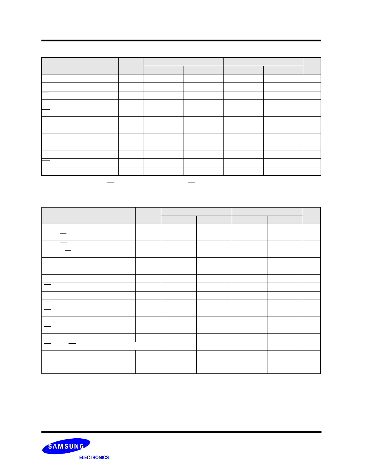
DC AND OPERATING CHARACTERISTICS(Recommended operating conditions otherwise noted.)
K9F1G08R0A K9F1G08U0A
Parameter Symbol Test Conditions
Min Typ Max Min Ty p Max
Page Read with
Operating
Serial Access
Current
Program ICC2 - - 10 20 - 15 30
Erase I
Stand-by Current(TTL) ISB1CE=VIH, WP=0V/VCC --1--1
Stand-by Current(CMOS) I
Input Leakage Current I
Output Leakage Current ILO VOUT=0 to Vcc(max) - - ±10 - - ±10
Input High Voltage V
Input Low Voltage, All inputs VIL* - -0.3 - 0.2xVcc -0.3 - 0.2xVcc
Output High Voltage Level V
Output Low Voltage Level
Output Low Current(R/B
NOTE : VIL can undershoot to -0.4V and VIH can overshoot to VCC +0.4V for durations of 20 ns or less.
)IOL(R/B)
tRC=30ns(50ns with 1.8V device),
I
CC1
CE=VIL
- 10 20 - 15 30
IOUT=0mA
CC3 - - 10 20 - 15 30
CE
SB2
LI VIN=0 to Vcc(max) - - ±10 - - ±10
IH* -0.8xVCC -
OH
OL
V
=VCC-0.2,
=0V/VCC
WP
K9F1G08R0A :IOH=-100µA
K9F1G08U0A :I
OH=-400µA
K9F1G08R0A :IOL=100uA
K9F1G08U0A :I
K9F1G08R0A :V
K9F1G08U0A :V
OL=2.1mA
OL=0.1V
OL=0.4V
- 10 50 - 10 50
V
CC
0.8xVcc -
Vcc
-0.1
+0.3
--2.4--
+0.3
--0.1--0.4
34- 810-mA
V
CC
Unit1.8V 3.3V
mA
µA
V
9
K9F1G08R0A
K9F1G08U0A
VALID BLOCK
Parameter Symbol Min Typ. Max Unit
K9F1G08X0A N
K9K2G08U1A
NOTE :
K9F1G08X0A may include invalid blocks when first shipped. Additional invalid blocks may develop while being used. The number of valid
1. The
blocks is presented with both cases of invalid blocks considered. Invalid blocks are defined as blocks that contain one or more bad bits. Do not erase
or program factory-marked bad blocks
2. The 1st block, which is placed on 00h block address, is guaranteed to be a valid block, does not require Error Correction up to 1K program/erase
cycles.
Each K9F1G08U0A chip in the K9K2G08U1A has Maximum 20 invalid blocks.
* :
AC TEST CONDITION
(K9F1G08X0A-XCB0 :TA=0 to 70°C, K9F1G08X0A-XIB0:TA=-40 to 85°C
K9F1G08R0A : Vcc=1.65V~1.95V, K9F1G08U0A : Vcc=2.7V~3.6V unless otherwise noted)
Input Pulse Levels 0V to Vcc 0V to Vcc
Input Rise and Fall Times 5ns 5ns
Input and Output Timing Levels Vcc/2 Vcc/2
Output Load 1 TTL GATE and CL=30pF 1 TTL GATE and CL=50pF
CAPACITANCE(TA=25°C, VCC=1.8V/3.3V, f=1.0MHz)
Input/Output Capacitance C
Input Capacitance C
NOTE : Capacitance is periodically sampled and not 100% tested.
MODE SELECTION
CLE ALE CE WE RE WP Mode
HLL HX
L H L H X Address Input(4clock)
HLL HH
L H L H H Address Input(4clock)
L L L H H Data Input
L L L H X Data Output
XXXXHX During Read(Busy)
XXXXXH During Program(Busy)
XXXXXH During Erase(Busy)
X
XXHXX
NOTE : 1. X can be VIL or VIH.
2. WP should be biased to CMOS high or CMOS low for standby.
Program / Erase Characteristics
Program Time
Dummy Busy Time for Cache Program
Number of Partial Program Cycles
in the Same Page
Block Erase Time t
NOTE : 1. Typical program time is defined as the time within which more than 50% of the whole pages are programmed at Vcc of 3.3V ans 25’C.
2. Max. time of tCBSY depends on timing between internal program completion and data in.
K9K2G08U1A FLASH MEMORY
VB 1004 - 1024 Blocks
VB
N
. Refer to the attached technical notes for appropriate management of invalid blocks.
Parameter K9F1G08R0A K9F1G08U0A
Item Symbol Test Condition Min Max Unit
I/O VIL=0V - 10 pF
IN VIN=0V - 10 pF
*1
X
X X X L Write Protect
Parameter Symbol Min Ty p Max Unit
Main Array
Spare Array - - 4 cycles
2008 - 2048 Blocks
Read Mode
Write Mode
(2)
0V/V
*1
PROG
t
*2
CBSY
t
Nop
BERS -23ms
Stand-by
CC
- 200 700 µs
- - 4 cycles
Command Input
Command Input
3 700
µs
10
K9F1G08R0A
K9F1G08U0A
AC Timing Characteristics for Command / Address / Data Input
Parameter Symbol
CLE setup Time
CLE Hold Time t
CE
setup Time
Hold Time tCH 10 5 - - ns
CE
WE
Pulse Width tWP 25 15 - - ns
ALE setup Time
ALE Hold Time t
Data setup Time
Data Hold Time t
Write Cycle Time t
WE
High Hold Time tWH 15 10 - - ns
ALE to Data Loading Time
NOTE : 1. The transition of the corresponding control pins must occur only once while WE is held low.
2. tADL is the time from the WE
3. For cache program operation, the whole AC Charcateristics must be same as that of K9F1G08R0A.
K9K2G08U1A FLASH MEMORY
Min Max
K9F1G08R0A K9F1G08U0A K9F1G08R0A K9F1G08U0A
*1
CLS
t
CLH 10 5 - - ns
*1
CS
t
*1
t
ALS
ALH 10 5 - - ns
*1
DS
t
DH 10 5 - - ns
WC 45 30 - - ns
*2
t
ADL
rising edge of final address cycle to the WE rising edge of first data cycle.
25 15 - - ns
35 20 - - ns
25 15 - - ns
20 15 - - ns
100
*2
100
*2
--ns
Unit
AC Characteristics for Operation
Parameter Symbol
K9F1G08R0A K9F1G08U0A K9F1G08R0A K9F1G08U0A
Data Transfer from Cell to Register tR - - 25 25 µs
ALE to RE
CLE to RE
Ready to RE
RE Pulse Width t
WE High to Busy t
Read Cycle Time t
RE
CE
RE
CE
RE
RE
Output Hi-Z to RE
RE
WE
Device Resetting Time
(Read/Program/Erase)
NOTE: 1. If reset command(FFh) is written at Ready state, the device goes into Busy for maximum 5us.
2. For cache program operation, the whole AC Charcateristics must be same as that of K9F1G08R0A.
Delay tAR 10 10 - - ns
Delay tCLR 10 10 - - ns
Low tRR 20 20 - - ns
RP 25 15 - - ns
WB - - 100 100 ns
RC 50 30 - - ns
Access Time tREA - - 30 20 ns
Access Time tCEA - - 45 35 ns
High to Output Hi-Z tRHZ - - 30 30 ns
High to Output Hi-Z tCHZ - - 20 20 ns
or CE High to Output hold tOH 15 15 - - ns
High Hold Time tREH 15 10 - - ns
Low tIR 00- -ns
High to WE Low tRHW 100 100 - - ns
High to RE Low tWHR 60 60 - - ns
t
RST --
Min Max
5/10/500
*1
5/10/500
*1
Unit
µs
11
K9F1G08R0A
K9F1G08U0A
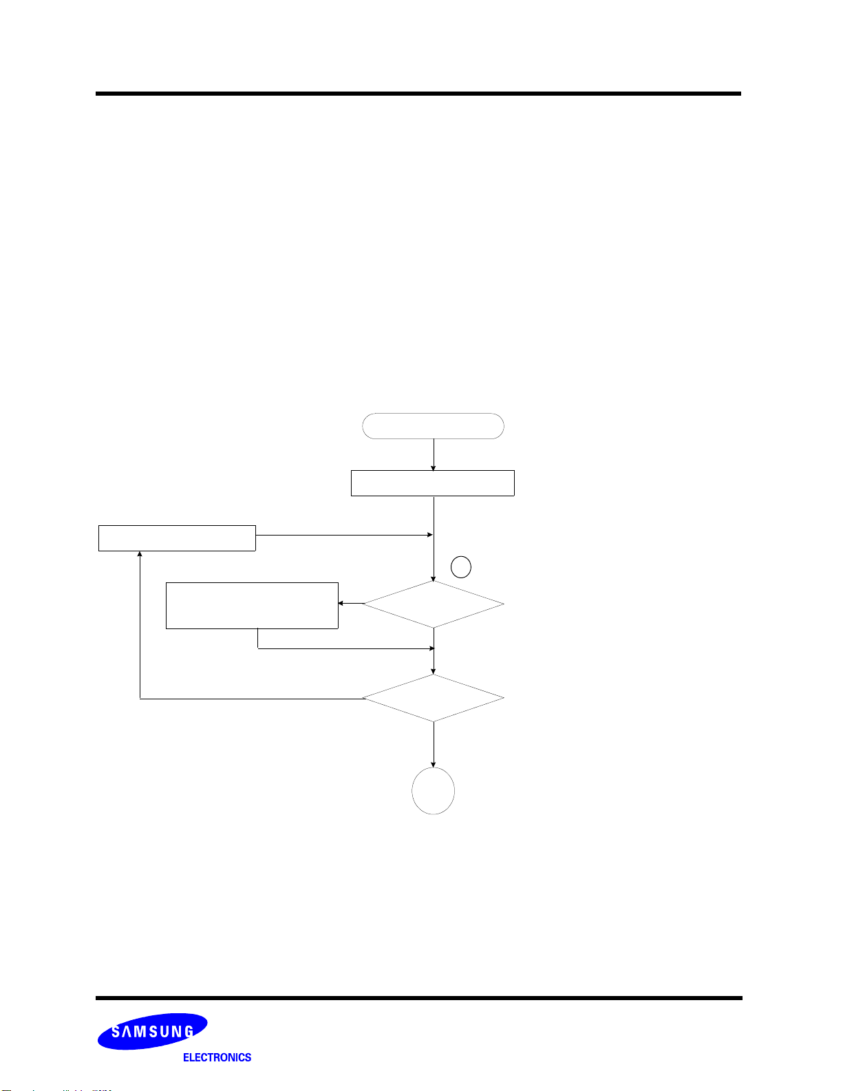
NAND Flash Technical Notes
Initial Invalid Block(s)
Initial invalid blocks are defined as blocks that contain one or more initial invalid bits whose reliability is not guaranteed by Samsung.
The information regarding the initial invalid block(s) is so called as the initial invalid block information. Devices with initial invalid
block(s) have the same quality level as devices with all valid blocks and have the same AC and DC characteristics. An initial invalid
block(s) does not affect the performance of valid block(s) because it is isolated from the bit line and the common source line by a
select transistor. The system design must be able to mask out the initial invalid block(s) via address mapping. The 1st block, which is
placed on 00h block address, is guaranteed to be a valid block, does not require Error Correction up to 1K program/erase cycles.
Identifying Initial Invalid Block(s)
All device locations are erased(FFh) except locations where the initial invalid block(s) information is written prior to shipping. The
initial invalid block(s) status is defined by the 1st byte in the spare area. Samsung makes sure that either the 1st or 2nd page of every
initial invalid block has non-FFh data at the column address of 2048. Since the initial invalid block information is also erasable in
most cases, it is impossible to recover the information once it has been erased. Therefore, the system must be able to recognize the
initial invalid block(s) based on the initial invalid block information and create the initial invalid block table via the following suggested
flow chart(Figure 3). Any intentional erasure of the initial invalid block information is prohibited.
K9K2G08U1A FLASH MEMORY
Start
Increment Block Address
Create (or update)
Initial Invalid Block(s) Table
Figure 3. Flow chart to create initial invalid block table.
Set Block Address = 0
No
No
Check "FFh
Yes
Last Block ?
Yes
End
Check "FFh" at the column address
of the 1st and 2nd page in the block
2048
*
12
 Loading...