

Samsung K9F1216U0A-PIB0, K9F1216U0A-PCB0, K9F1216U0A-DIB0, K9F1216U0A-DCB0, K9F1216Q0A-HIB0 Datasheet
...
San 16 Banwol-Ri
Taean-Eup Hwasung- City
Kyungki Do, Korea
Tel.) 82 - 31 - 208 - 6463
Fax.) 82 - 31 -208 - 6799
March. 2003
ELECTRONICS
1
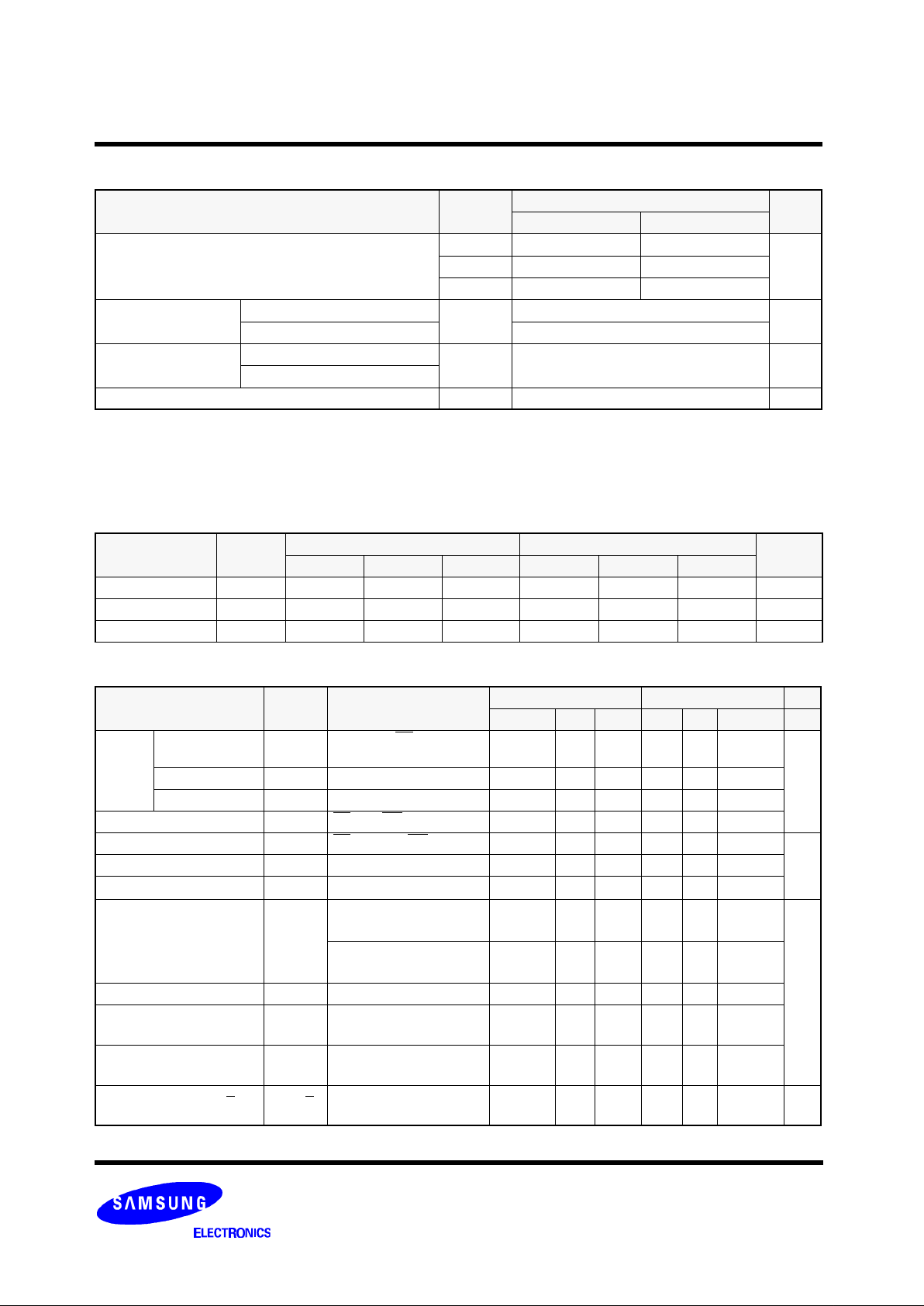
512Mb/256Mb 1.8V NAND Flash Errata
Description : Some of AC characteristics are not meeting the specification.
> AC characteristics : Refer to Table
Affected Products : K9F1208Q0A-XXB0, K9F1216Q0A-XXB0
K9F5608Q0C-XXB0, K9F5616Q0C-XXB0
K9K1208Q0C-XXB0, K9K1216Q0C-XXB0
Improvement schedule : The components without this restriction will
be available from work week 23 or after.
Workaround : Relax the relevant timing parameters according to the table.
Sincerely,
chwoosun@sec.samsung.com
Product Planning & Application Eng.
Memory Division
Samsung Electronics Co.
Table
Parameters
Specification
Relaxed Condition
tWC
45
80
tWH
15
20
tWP
25
60
tRC
50
80
tREH
15
20
tRP
25
60
tREA
30
60
UNIT : ns
tCEA
45
75
K9F1216U0A-YCB0,YIB0,PCB0,PIB0
FLASH MEMORY
1
K9F1216U0A-DCB0,DIB0,HCB0,HIB0
K9F1208U0A-YCB0,YIB0,PCB0,PIB0
K9F1208U0A-DCB0,DIB0,HCB0,HIB0
K9F1208Q0A-DCB0,DIB0,HCB0,HIB0 K9F1216Q0A-DCB0,DIB0,HCB0,HIB0
K9F1208U0A-VCB0,VIB0,FCB0,FIB0
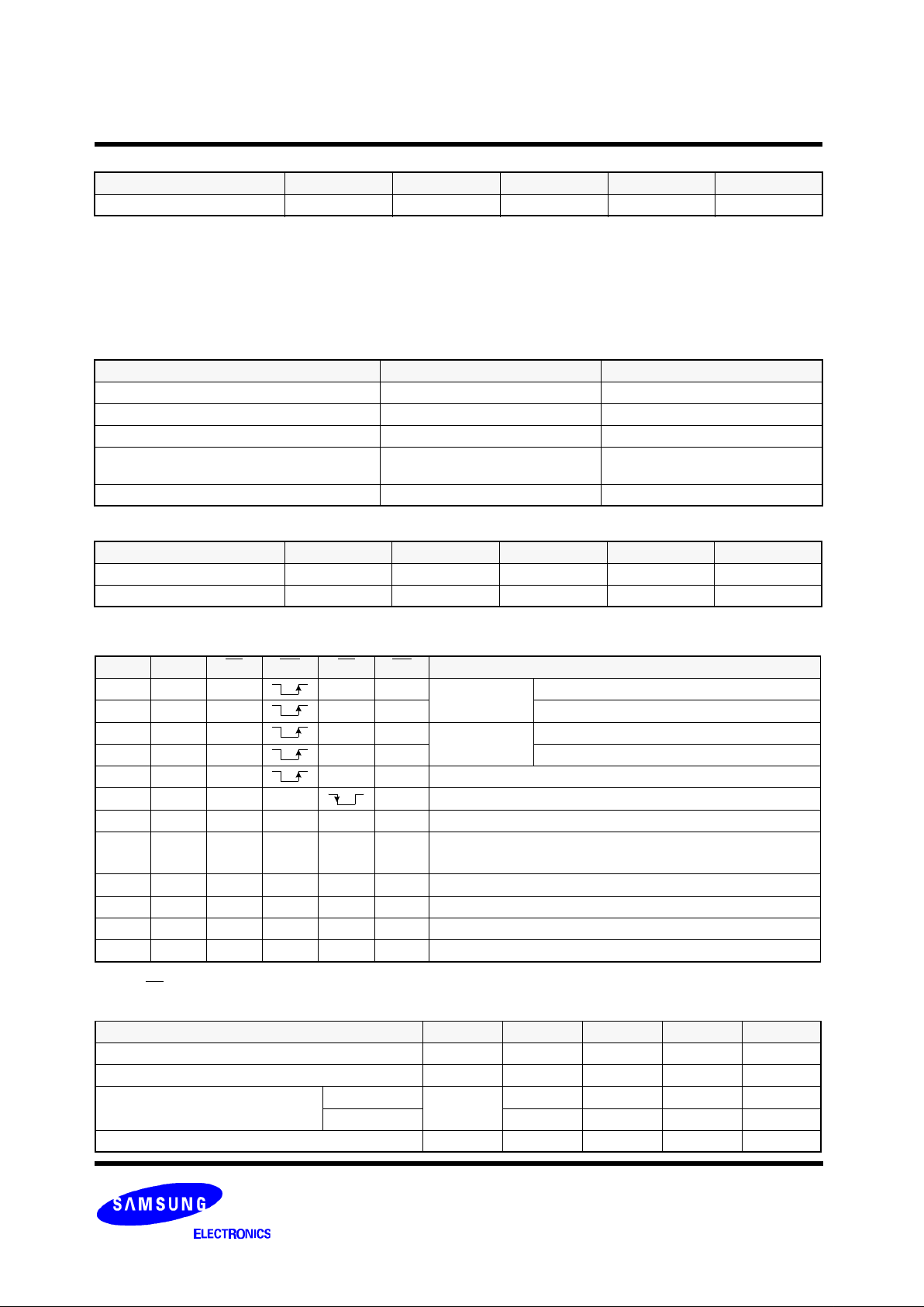
Document Title
64M x 8 Bit , 32M x 16 Bit NAND Flash Memory
Revision History
The attached datasheets are prepared and approved by SAMSUNG Electronics. SAMSUNG Electronics CO., LTD. reserve the right
to change the specifications. SAMSUNG Electronics will evaluate and reply to your requests and questions about device. If you have
any questions, please contact the SAMSUNG branch office near you.
Revision No.
0.0
0.1
0.2
0.3
0.4
0.5
0.6
0.7
0.8
0.9
Remark
Preliminary
History
Initial issue.
TBGA(K9F12XXX0A-DCB0/DIB0) size information is changed.
(before) 9 x 11 /0.8mm pitch , Width 1.0 mm
(after ) To Be Decided.
TBGA(K9F12XXX0A-DCB0/DIB0) size information is changed.
(before) 9 x 11 /0.8mm pitch , Width 1.0 mm, to
(after) 8.5 x 15 /0.8mm pitch, Width 1.0mm
Pin numbering includes TBGA Dummy ball . (Page5)
Pin numbering excludes TBGA Dummy ball . (Page5)
Pin assignment of TBGA dummy ball is changed.
(before) DNU --> (after) N.C
1. Add the Rp vs tr ,tf & Rp vs ibusy graph for 1.8V device (Page 43)
2. Add the data protection Vcc guidence for 1.8V device - below about
1.1V. (Page 44)
The min. Vcc value 1.8V devices is changed.
K9F12XXQ0A : Vcc 1.65V~1.95V --> 1.70V~1.95V
Pb-free Package is added.
K9F1208U0A-FCB0,FIB0
K9F1208Q0A-HCB0,HIB0
K9F1216U0A-HCB0,HIB0
K9F1216U0A-PCB0,PIB0
K9F1216Q0A-HCB0,HIB0
K9F1208U0A-HCB0,HIB0
K9F1208U0A-PCB0,PIB0
Errata is added.(Front Page)-K9F12XXQ0A
tWC tWH tWP tRC tREH tRP tREA tCEA
Specification 45 15 25 50 15 25 30 45
Relaxed value 60 20 40 60 20 40 40 55
New definition of the number of invalid blocks is added.
(Minimum 1004 valid blocks are guaranteed for each contiguous 128Mb
memory space.)
Draft Date
Apr. 25th 2002
May. 9th 2002
July, 10th 2002
Aug, 10th 2002
Oct, 21th 2002
Nov, 21th 2002
Mar. 5th 2003
Mar. 13rd 2003
Mar. 17th 2003
Apr. 4th 2003
Note : For more detailed features and specifications including FAQ, please refer to Samsung’s Flash web site.
http://www.intl.samsungsemi.com/Memory/Flash/datasheets.html
K9F1216U0A-YCB0,YIB0,PCB0,PIB0
FLASH MEMORY
2
K9F1216U0A-DCB0,DIB0,HCB0,HIB0
K9F1208U0A-YCB0,YIB0,PCB0,PIB0
K9F1208U0A-DCB0,DIB0,HCB0,HIB0
K9F1208Q0A-DCB0,DIB0,HCB0,HIB0 K9F1216Q0A-DCB0,DIB0,HCB0,HIB0
K9F1208U0A-VCB0,VIB0,FCB0,FIB0
GENERAL DESCRIPTION
FEATURES
• Voltage Supply
- 1.8V device(K9F12XXQ0A) : 1.70~1.95V
- 3.3V device(K9F12XXU0A) : 2.7 ~ 3.6 V
• Organization
- Memory Cell Array
- X8 device(K9F1208X0A) : (64M + 2048K)bit x 8 bit
- X16 device(K9F1216X0A) : (32M + 1024K)bit x 16bit
- Data Register
- X8 device(K9F1208X0A) : (512 + 16)bit x 8bit
- X16 device(K9F1216X0A) : (256 + 8)bit x16bit
• Automatic Program and Erase
- Page Program
- X8 device(K9F1208X0A) : (512 + 16)Byte
- X16 device(K9F1216X0A) : (256 + 8)Word
- Block Erase :
- X8 device(K9F1208X0A) : (16K + 512)Byte
- X16 device(K9F1216X0A) : ( 8K + 256)Word
• Page Read Operation
- Page Size
- X8 device(K9F1208X0A) : (512 + 16)Byte
- X16 device(K9F1216X0A) : (256 + 8)Word
- Random Access : 12µs(Max.)
- Serial Page Access : 50ns(Min.)
64M x 8 Bit / 32M x 16 Bit NAND Flash Memory
• Fast Write Cycle Time
- Program time : 200µs(Typ.)
- Block Erase Time : 2ms(Typ.)
• Command/Address/Data Multiplexed I/O Port
• Hardware Data Protection
- Program/Erase Lockout During Power Transitions
• Reliable CMOS Floating-Gate Technology
- Endurance : 100K Program/Erase Cycles
- Data Retention : 10 Years
• Command Register Operation
• Intelligent Copy-Back
• Unique ID for Copyright Protection
• Package
- K9F12XXU0A-YCB0/YIB0
48 - Pin TSOP I (12 x 20 / 0.5 mm pitch)
- K9F12XXX0A-DCB0/DIB0
63- Ball TBGA
- K9F1208U0A-VCB0/VIB0
48 - Pin WSOP I (12X17X0.7mm)
- K9F12XXU0A-PCB0/PIB0
48 - Pin TSOP I (12 x 20 / 0.5 mm pitch)- Pb-free Package
- K9F12XXX0A-HCB0/HIB0
63- Ball TBGA - Pb-free Package
- K9F1208U0A-FCB0/FIB0
48 - Pin WSOP I (12X17X0.7mm)- Pb-free Package
* K9F1208U0A-V,F(WSOPI ) is the same device as
K9F1208U0A-Y,P(TSOP1) except package type.
Offered in 64Mx8bit or 32Mx16bit, the K9F12XXX0A is 512M bit with spare 16M bit capacity. The device is offered in 1.8V or 3.3V
Vcc. Its NAND cell provides the most cost-effective solutIon for the solid state mass storage market. A program operation can be
performed in typical 200µs on the 528-byte(X8 device) or 264-word(X16 device) page and an erase operation can be performed in
typical 2ms on a 16K-byte(X8 device) or 8K-word(X16 device) block. Data in the page can be read out at 50ns cycle time per word.
The I/O pins serve as the ports for address and data input/output as well as command input. The on-chip write control automates all
program and erase functions including pulse repetition, where required, and internal verification and margining of data. Even the
write-intensive systems can take advantage of the K9F12XXX0A′s extended reliability of 100K program/erase cycles by providing
ECC(Error Correcting Code) with real time mapping-out algorithm.
The K9F12XXX0A is an optimum solution for large nonvolatile storage applications such as solid state file storage and other portable
applications requiring non-volatility.
PRODUCT LIST
Part Number Vcc Range Organization PKG Type
K9F1208Q0A-D,H
1.70 ~ 1.95V
X8
TBGA
K9F1216Q0A-D,H X16
K9F1208U0A-Y,P
2.7 ~ 3.6V
X8
TSOP1
K9F1208U0A-D,H TBGA
K9F1208U0A-V,F WSOP1
K9F1216U0A-Y,P
X16
TSOP1
K9F1216U0A-D,P TBGA
K9F1216U0A-YCB0,YIB0,PCB0,PIB0
FLASH MEMORY
3
K9F1216U0A-DCB0,DIB0,HCB0,HIB0
K9F1208U0A-YCB0,YIB0,PCB0,PIB0
K9F1208U0A-DCB0,DIB0,HCB0,HIB0
K9F1208Q0A-DCB0,DIB0,HCB0,HIB0 K9F1216Q0A-DCB0,DIB0,HCB0,HIB0
K9F1208U0A-VCB0,VIB0,FCB0,FIB0
PIN CONFIGURATION (TSOP1)
K9F12XXU0A-YCB0,PCB0/YIB0,PIB0
N.C
N.C
N.C
N.C
N.C
N.C
R/B
RE
CE
N.C
N.C
Vcc
Vss
N.C
N.C
CLE
ALE
WE
WP
N.C
N.C
N.C
N.C
N.C
Vss
I/O15
I/O7
I/O14
I/O6
I/O13
I/O5
I/O12
I/O4
N.C
N.C
Vcc
N.C
N.C
N.C
I/O11
I/O3
I/O10
I/O2
I/O9
I/O1
I/O8
I/O0
Vss
1
2
3
4
5
6
7
8
9
10
11
12
13
14
15
16
17
18
19
20
21
22
23
24
48
47
46
45
44
43
42
41
40
39
38
37
36
35
34
33
32
31
30
29
28
27
26
25
N.C
N.C
N.C
N.C
N.C
N.C
R/B
RE
CE
N.C
N.C
Vcc
Vss
N.C
N.C
CLE
ALE
WE
WP
N.C
N.C
N.C
N.C
N.C
N.C
N.C
N.C
N.C
I/O7
I/O6
I/O5
I/O4
N.C
N.C
N.C
Vcc
Vss
N.C
N.C
N.C
I/O3
I/O2
I/O1
I/O0
N.C
N.C
N.C
N.C
X8X16 X16X8
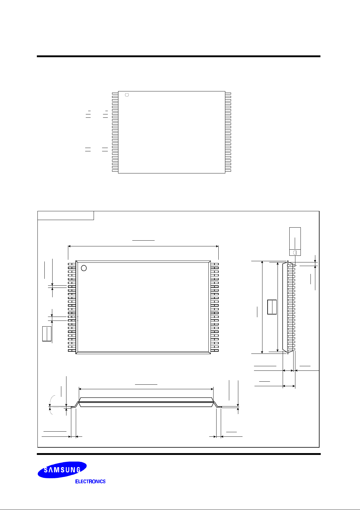
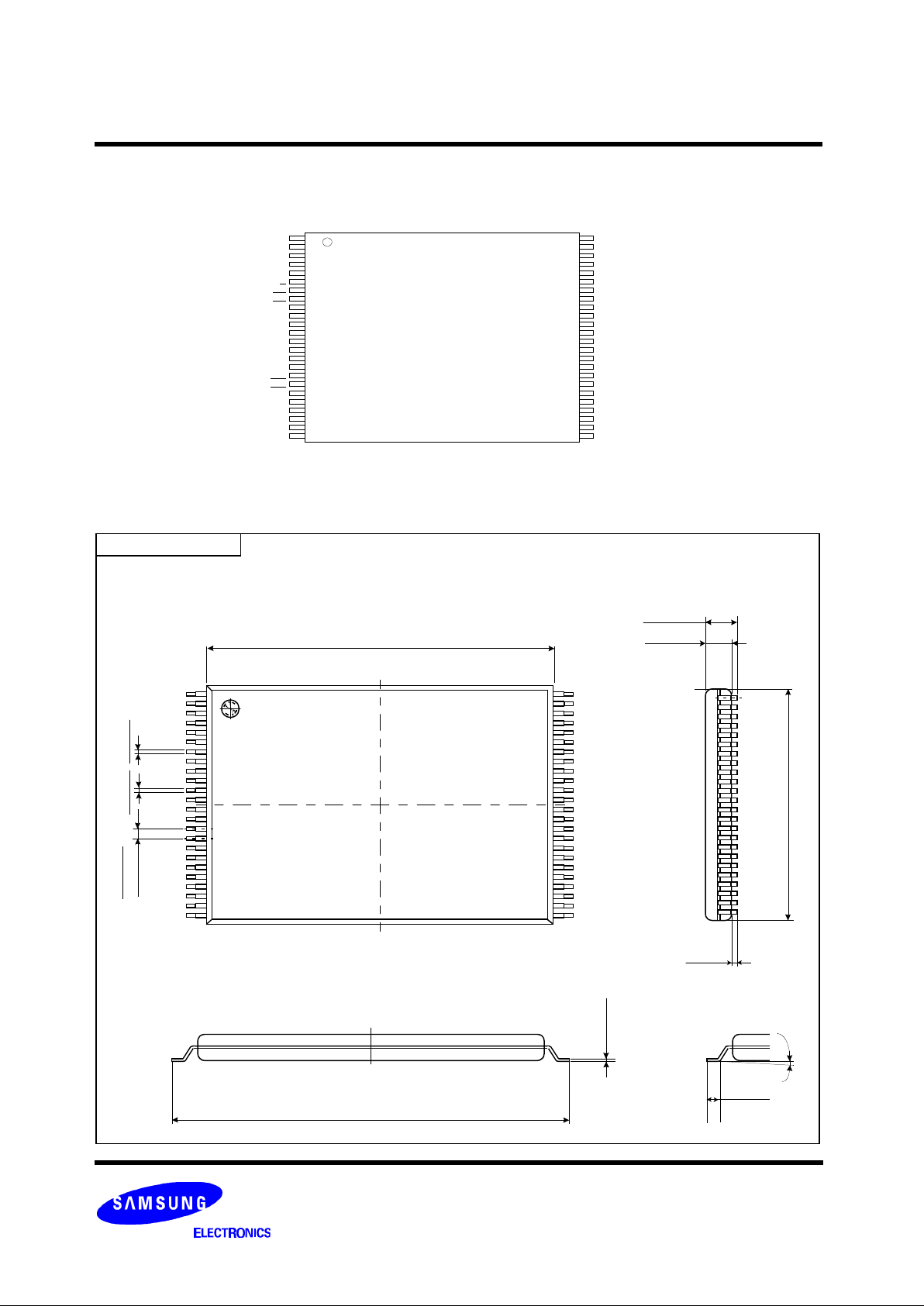
PACKAGE DIMENSIONS
48-PIN LEAD/LEAD FREE PLASTIC THIN SMALL OUT-LINE PACKAGE TYPE(I)
48 - TSOP1 - 1220F
Unit :mm/Inch
0.787±0.008
20.00±0.20
#1
#24
0.20
+0.07
-0.03
0.008
+0.003
-0.001
0.50
0.0197
#48
#25
0.488
12.40
MAX
12.00
0.472
0.10
0.004
MAX
0.25
0.010
( )
0.039±0.002
1.00±0.05
0.002
0.05
MIN
0.047
1.20
MAX
0.45~0.75
0.018~0.030
0.724±0.004
18.40±0.10
0~8¡Æ
0.010
0.25
TYP
0.125
+0.075
0.035
0.005
+0.003
-0.001
0.50
0.020
( )
K9F1216U0A-YCB0,YIB0,PCB0,PIB0
FLASH MEMORY
4
K9F1216U0A-DCB0,DIB0,HCB0,HIB0
K9F1208U0A-YCB0,YIB0,PCB0,PIB0
K9F1208U0A-DCB0,DIB0,HCB0,HIB0
K9F1208Q0A-DCB0,DIB0,HCB0,HIB0 K9F1216Q0A-DCB0,DIB0,HCB0,HIB0
K9F1208U0A-VCB0,VIB0,FCB0,FIB0
K9F12XXX0A-DCB0,HCB0/DIB0,HIB0
R/B/WE/CEVssALE/WP
/RE CLE
NCNC
NC NC
Vcc
NCNC I/O0
I/O1NC NC VccQ I/O5 I/O7
VssI/O6I/O4I/O3I/O2Vss
NC
NC
NC
NC NC
NC
NC NC
NCNCNC
NC
NC NC NC
NC
NC
NC
NC
NC
N.C
N.C N.C
N.C
N.C N.C
N.C
N.C
N.C N.C
N.CN.C
N.C N.C
N.C
N.C
N.C N.C
N.C
N.C N.C
N.C
N.C
N.C N.C
N.CN.C
N.C N.C
N.C
R/B/WE/CEVssALE/WP
/RE CLE
I/O7I/O5
I/O12 IO14
Vcc
I/O10I/O8 I/O1
I/O9I/O0 I/O3 VccQ I/O6 I/O15
VssI/O13I/O4I/O11I/O2Vss
NC
NC
NC
NC NC
NC
NC NC
NCNCNC
NC
NC NC NC
NC
NC
NC
NC
NC
X16
X8
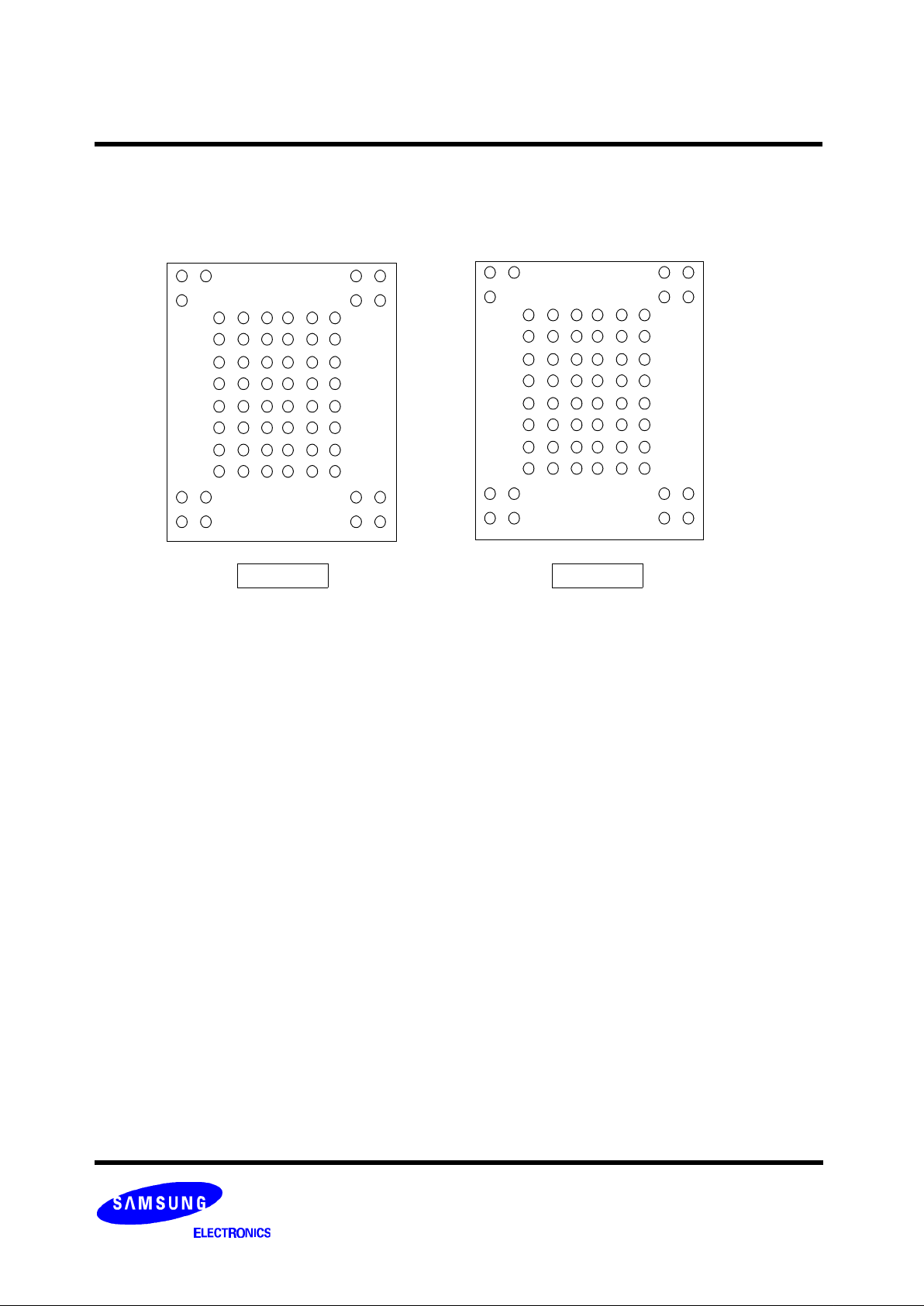
PIN CONFIGURATION (TBGA)
3 4 5 6 1 2
A
B
C
D
G
E
F
H
3 4 5 6 1 2
A
B
C
D
G
E
F
H
Top View Top View
K9F1216U0A-YCB0,YIB0,PCB0,PIB0
FLASH MEMORY
5
K9F1216U0A-DCB0,DIB0,HCB0,HIB0
K9F1208U0A-YCB0,YIB0,PCB0,PIB0
K9F1208U0A-DCB0,DIB0,HCB0,HIB0
K9F1208Q0A-DCB0,DIB0,HCB0,HIB0 K9F1216Q0A-DCB0,DIB0,HCB0,HIB0
K9F1208U0A-VCB0,VIB0,FCB0,FIB0
8.50±0.10
#A1
Side View
Top View
63-Ball TBGA (measured in millimeters)
0.90±0.10
0.45±0.05
4 3 2 1
A
B
C
D
G
Bottom View
15.00±0.10
63-∅0.45±0.05
0.80 x 7= 5.60
15.00±0.10
0.80 x 5= 4.00
0.80
0.32±0.05
0.10MAX
B
A
2.80
2.00
8.50±0.10
(Datum B)
(Datum A)
0.20
M
A B
∅
0.80
0.80 x 11= 8.80
0.80 x 9= 7.20
6 5
15.00±0.10
E
F
H
#A1 INDEX MARK(OPTIONAL)
K9F1216U0A-YCB0,YIB0,PCB0,PIB0
FLASH MEMORY
6
K9F1216U0A-DCB0,DIB0,HCB0,HIB0
K9F1208U0A-YCB0,YIB0,PCB0,PIB0
K9F1208U0A-DCB0,DIB0,HCB0,HIB0
K9F1208Q0A-DCB0,DIB0,HCB0,HIB0 K9F1216Q0A-DCB0,DIB0,HCB0,HIB0
K9F1208U0A-VCB0,VIB0,FCB0,FIB0
PIN CONFIGURATION (WSOP1)
K9F1208U0A-VCB0,FCB0/VIB0,FIB0
PACKAGE DIMENSIONS
48-PIN LEAD/LEAD FREE PLASTIC VERY VERY THIN SMALL OUT-LINE PACKAGE TYPE (I)
48 - WSOP1 - 1217F
Unit :mm
15.40±0.10
#1
#24
0.20
+0.07
-0.03
0.16
+0.07
-0.03
0.50TYP
(0.50±0.06)
#48
#25
12.00±0.10
0.10
+0.075
-0.035
0.58±0.04
0.70 MAX
(0.1Max)
17.00±0.20
0
°
~
8
°
0.45~0.75
1
2
3
4
5
6
7
8
9
10
11
12
13
14
15
16
17
18
19
20
21
22
23
24
48
47
46
45
44
43
42
41
40
39
38
37
36
35
34
33
32
31
30
29
28
27
26
25
N.C
N.C
DNU
N.C
N.C
N.C
R/B
RE
CE
DNU
N.C
Vcc
Vss
N.C
DNU
CLE
ALE
WE
WP
N.C
N.C
DNU
N.C
N.C
N.C
N.C
DNU
N.C
I/O7
I/O6
I/O5
I/O4
N.C
DNU
N.C
Vcc
Vss
N.C
DNU
N.C
I/O3
I/O2
I/O1
I/O0
N.C
DNU
N.C
N.C
K9F1216U0A-YCB0,YIB0,PCB0,PIB0
FLASH MEMORY
7
K9F1216U0A-DCB0,DIB0,HCB0,HIB0
K9F1208U0A-YCB0,YIB0,PCB0,PIB0
K9F1208U0A-DCB0,DIB0,HCB0,HIB0
K9F1208Q0A-DCB0,DIB0,HCB0,HIB0 K9F1216Q0A-DCB0,DIB0,HCB0,HIB0
K9F1208U0A-VCB0,VIB0,FCB0,FIB0
PIN DESCRIPTION
NOTE : Connect all VCC and VSS pins of each device to common power supply outputs.
Do not leave VCC or VSS disconnected.
Pin Name Pin Function
I/O0 ~ I/O7
(K9F1208X0A)
I/O0 ~ I/O15
(K9F1216X0A)
DATA INPUTS/OUTPUTS
The I/O pins are used to input command, address and data, and to output data during read operations. The
I/O pins float to high-z when the chip is deselected or when the outputs are disabled.
I/O8 ~ I/O15 are used only in X16 organization device. Since command input and address input are x8 operation, I/O8 ~ I/O15 are not used to input command & address. I/O8 ~ I/O15 are used only for data input and
output.
CLE
COMMAND LATCH ENABLE
The CLE input controls the activating path for commands sent to the command register. When active high,
commands are latched into the command register through the I/O ports on the rising edge of the WE signal.
ALE
ADDRESS LATCH ENABLE
The ALE input controls the activating path for address to the internal address registers. Addresses are
latched on the rising edge of WE with ALE high.
CE
CHIP ENABLE
The CE input is the device selection control. When the device is in the Busy state, CE high is ignored, and
the device does not return to standby mode in program or erase opertion. Regarding CE control during read
operation, refer to ’Page read’ section of Device operation .
RE
READ ENABLE
The RE input is the serial data-out control, and when active drives the data onto the I/O bus. Data is valid
tREA after the falling edge of RE which also increments the internal column address counter by one.
WE
WRITE ENABLE
The WE input controls writes to the I/O port. Commands, address and data are latched on the rising edge of
the WE pulse.
WP
WRITE PROTECT
The WP pin provides inadvertent write/erase protection during power transitions. The internal high voltage
generator is reset when the WP pin is active low.
R/B
READY/BUSY OUTPUT
The R/B output indicates the status of the device operation. When low, it indicates that a program, erase or
random read operation is in process and returns to high state upon completion. It is an open drain output and
does not float to high-z condition when the chip is deselected or when outputs are disabled.
VccQ
OUTPUT BUFFER POWER
VCCQ is the power supply for Output Buffer.
VccQ is internally connected to Vcc, thus should be biased to Vcc.
Vcc
POWER
VCC is the power supply for device.
Vss GROUND
N.C
NO CONNECTION
Lead is not internally connected.
DNU
DO NOT USE
Leave it disconnected.
K9F1216U0A-YCB0,YIB0,PCB0,PIB0
FLASH MEMORY
8
K9F1216U0A-DCB0,DIB0,HCB0,HIB0
K9F1208U0A-YCB0,YIB0,PCB0,PIB0
K9F1208U0A-DCB0,DIB0,HCB0,HIB0
K9F1208Q0A-DCB0,DIB0,HCB0,HIB0 K9F1216Q0A-DCB0,DIB0,HCB0,HIB0
K9F1208U0A-VCB0,VIB0,FCB0,FIB0
512Byte 16 Byte
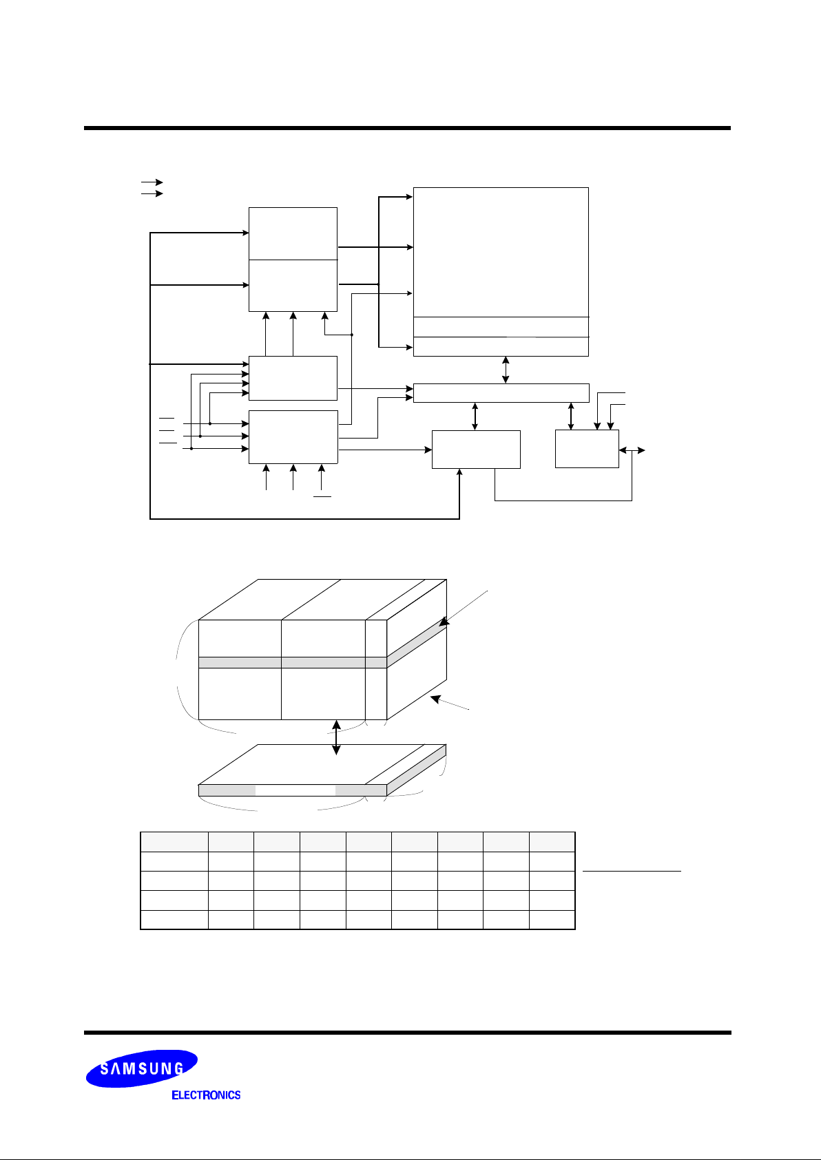
Figure 1-1. K9F1208X0A (X8) FUNCTIONAL BLOCK DIAGRAM
Figure 2-1. K9F1208X0A (X8) ARRAY ORGANIZATION
VCC
X-Buffers
512M + 16M Bit
Command
NAND Flash
ARRAY
(512 + 16)Byte x 131072
Y-Gating
Page Register & S/A
I/O Buffers & Latches
Latches
& Decoders
Y-Buffers
Latches
& Decoders
Register
Control Logic
& High Voltage
Generator
Global Buffers
Output
Driver
VSS
A9 - A25
A0 - A7
Command
CE
RE
WE
WP
I/0 0
I/0 7
VCC/VCCQ
VSS
A8
1st half Page Register
(=256 Bytes)
2nd half Page Register
(=256 Bytes)
128K Pages
(=4,096 Blocks)
512 Byte
8 bit
16 Byte
1 Block =32 Pages
= (16K + 512) Byte
I/O 0 ~ I/O 7
1 Page = 528 Byte
1 Block = 528 Byte x 32 Pages
= (16K + 512) Byte
1 Device = 528Bytes x 32Pages x 4096 Blocks
= 528 Mbits
Column Address
Row Address
(Page Address)
Page Register
CLE ALE
NOTE : Column Address : Starting Address of the Register.
00h Command(Read) : Defines the starting address of the 1st half of the register.
01h Command(Read) : Defines the starting address of the 2nd half of the register.
* A8 is set to "Low" or "High" by the 00h or 01h Command.
* L must be set to "Low".
* The device ignores any additional input of address cycles than reguired.
I/O 0 I/O 1 I/O 2 I/O 3 I/O 4 I/O 5 I/O 6 I/O 7
1st Cycle A0 A1 A2 A3 A4 A5 A6 A7
2nd Cycle A9 A10 A11 A12 A13 A14 A15 A16
3rd Cycle A17 A18 A19 A20 A21 A22 A23 A24
4th Cycle A25 *L *L *L *L *L *L *L
K9F1216U0A-YCB0,YIB0,PCB0,PIB0
FLASH MEMORY
9
K9F1216U0A-DCB0,DIB0,HCB0,HIB0
K9F1208U0A-YCB0,YIB0,PCB0,PIB0
K9F1208U0A-DCB0,DIB0,HCB0,HIB0
K9F1208Q0A-DCB0,DIB0,HCB0,HIB0 K9F1216Q0A-DCB0,DIB0,HCB0,HIB0
K9F1208U0A-VCB0,VIB0,FCB0,FIB0
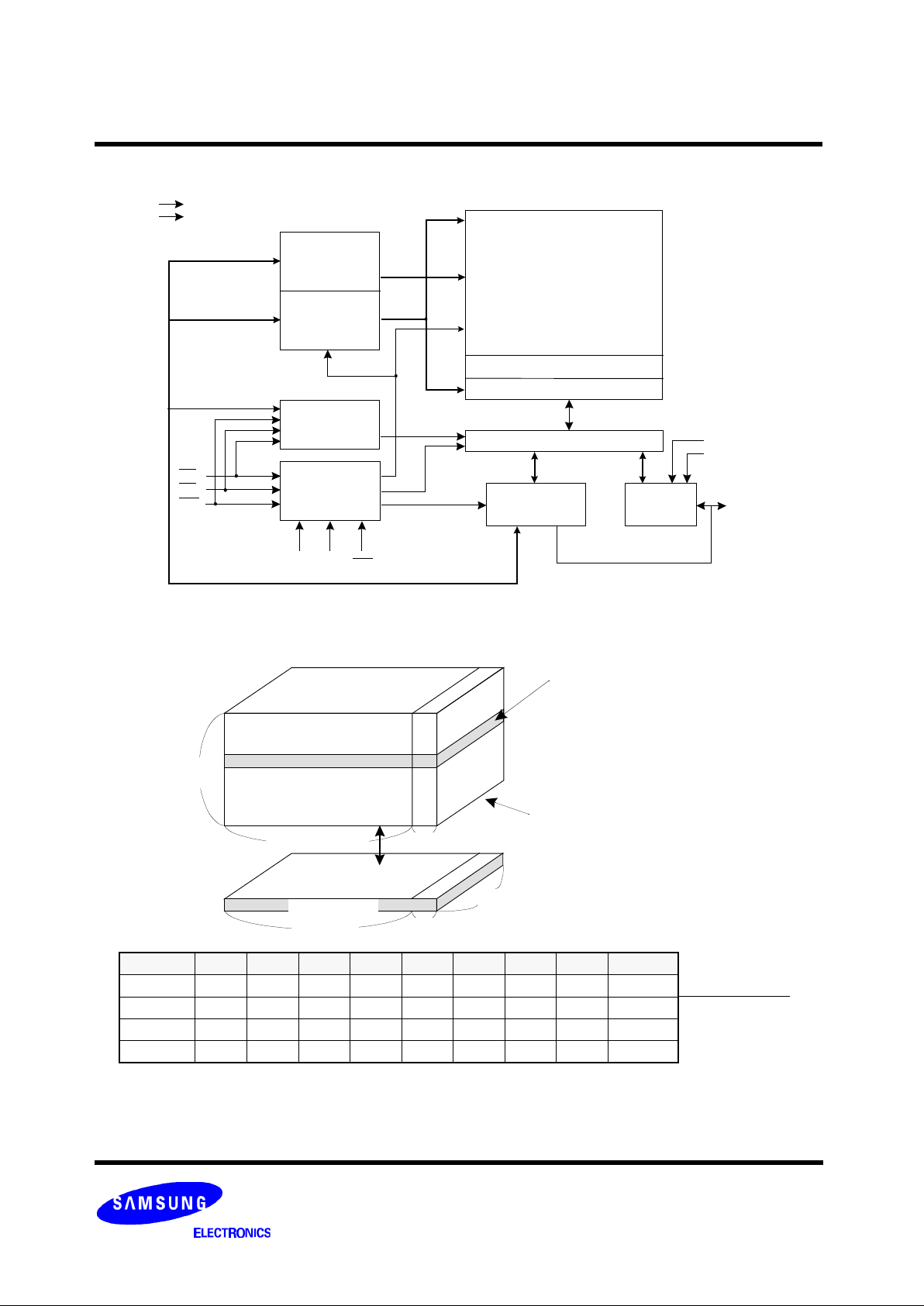
256Word 8 Word
Figure 2-2. K9F1216X0A (X16) ARRAY ORGANIZATION
NOTE : Column Address : Starting Address of the Register.
* L must be set to "Low".
I/O 0 I/O 1 I/O 2 I/O 3 I/O 4 I/O 5 I/O 6 I/O 7 I/O8 to 15
1st Cycle A0 A1 A2 A3 A4 A5 A6 A7
L*
2nd Cycle A9 A10 A11 A12 A13 A14 A15 A16
L*
3rd Cycle A17 A18 A19 A20 A21 A22 A23 A24
L*
4th Cycle A25
L* L* L* L* L* L* L* L*
Page Register
(=256 Words)
128K Pages
(=4,096 Blocks)
256 Word
16 bit
8 Word
1 Block =32 Pages
= (8K + 256) Word
I/O 0 ~ I/O 15
1 Page = 264 Word
1 Block = 264 Word x 32 Pages
= (8K + 256) Word
1 Device = 264Words x 32Pages x 4096 Blocks
= 528 Mbits
Column Address
Row Address
(Page Address)
Page Register
Figure 1-2. K9F1216X0A (X16) FUNCTIONAL BLOCK DIAGRAM
VCC
X-Buffers
5126M + 16M Bit
Command
NAND Flash
ARRAY
(256 + 8)Word x 131072
Y-Gating
Page Register & S/A
I/O Buffers & Latches
Latches
& Decoders
Y-Buffers
Latches
& Decoders
Register
Control Logic
& High Voltage
Generator
Global Buffers
Output
Driver
VSS
A9 - A25
A0 - A7
Command
CE
RE
WE
WP
I/0 0
I/0 15
VCC/VCCQ
VSS
CLE ALE
K9F1216U0A-YCB0,YIB0,PCB0,PIB0
FLASH MEMORY
10
K9F1216U0A-DCB0,DIB0,HCB0,HIB0
K9F1208U0A-YCB0,YIB0,PCB0,PIB0
K9F1208U0A-DCB0,DIB0,HCB0,HIB0
K9F1208Q0A-DCB0,DIB0,HCB0,HIB0 K9F1216Q0A-DCB0,DIB0,HCB0,HIB0
K9F1208U0A-VCB0,VIB0,FCB0,FIB0
Product Introduction
The K9F1208X0A is a 528Mbit(553,648,218 bit) memory organized as 131,072 rows(pages) by 528 columns. Spare sixteen columns
are located from column address of 512 to 527. A 528-byte data register is connected to memory cell arrays accommodating data
transfer between the I/O buffers and memory during page read and page program operations. The memory array is made up of 16
cells that are serially connected to form a NAND structure. Each of the 16 cells resides in a different page. A block consists of two
NAND structures. A NAND structure consists of 16 cells. Total 16896 NAND cells reside in a block. The array organization is shown
in Figure 2. The program and read operations are executed on a page basis, while the erase operation is executed on a block basis.
The memory array consists of 4,096 separately erasable 16K-byte blocks. It indicates that the bit by bit erase operation is prohibited
on the K9F1208X0A.
The K9F1208X0A has addresses multiplexed into 8 I/O's. This scheme dramatically reduces pin counts and allows systems upgrades
to future densities by maintaining consistency in system board design. Command, address and data are all written through I/O's by
bringing WE to low while CE is low. Data is latched on the rising edge of WE. Command Latch Enable(CLE) and Address Latch
Enable(ALE) are used to multiplex command and address respectively, via the I/O pins. The 64M byte physical space requires 26
addresses, thereby requiring four cycles for byte-level addressing: column address, low row address and high row address, in that
order. Page Read and Page Program need the same four address cycles following the required command input. In Block Erase operation, however, only the three row address cycles are used. Device operations are selected by writing specific commands into the
command register. Table 1 defines the specific commands of the K9F1208X0A.
The device provides simultaneous program/erase capability up to four pages/blocks. By dividing the memory array into four 128Mbit
separate planes, simultaneous multi-plane operation dramatically increases program/erase performance by 4X while still maintaining
the conventional 512 byte(X8 device) or 256 word(X16 device) structure.
The extended pass/fail status for multi-plane program/erase allows system software to quickly identify the failing page/block out of
selected multiple pages/blocks. Usage of multi-plane operations will be described further throughout this document.
In addition to the enhanced architecture and interface, the device incorporates copy-back program feature from one page to another
of the same plane without the need for transporting the data to and from the external buffer memory. Since the time-consuming burstreading and data-input cycles are removed, system performance for solid-state disk application is significantly increased.
The device includes one block sized OTP(One Time Programmable), which can be used to increase system security or to provide
identification capabilities. Detailed information can be obtained by contact with Samsung.
Table 1. Command Sets
NOTE : 1. The 00h command defines starting address of the 1st half of registers.
The 01h command defines starting address of the 2nd half of registers.
After data access on the 2nd half of register by the 01h command, the status pointer is
automatically moved to the 1st half register(00h) on the next cycle.
2. Page Program(True) and Copy-Back Program(True) are available on 1 plane operation.
Page Program(Dummy) and Copy-Back Program(Dummy) are available on the 2nd,3rd,4th plane of multi plane operation.
3. The 71h command should be used for read status of Multi Plane operation.
Caution : Any undefined command inputs are prohibited except for above command set of Table 1.
Function 1st. Cycle 2nd. Cycle 3rd. Cycle
Acceptable Command
during Busy
Read 1
00h/01h
(1)
- Read 2 50h - Read ID 90h - Reset FFh - - O
Page Program (True)
(2)
80h 10h -
Page Program (Dummy)
(2)
80h 11h -
Copy-Back Program(True)
(2)
00h 8Ah 10h
Copy-Back Program(Dummy)
(2)
03h 8Ah 11h
Block Erase 60h D0h Multi-Plane Block Erase 60h----60h D0h Read Status 70h - - O
Read Multi-Plane Status
71h
(3)
- - O
K9F1216U0A-YCB0,YIB0,PCB0,PIB0
FLASH MEMORY
11
K9F1216U0A-DCB0,DIB0,HCB0,HIB0
K9F1208U0A-YCB0,YIB0,PCB0,PIB0
K9F1208U0A-DCB0,DIB0,HCB0,HIB0
K9F1208Q0A-DCB0,DIB0,HCB0,HIB0 K9F1216Q0A-DCB0,DIB0,HCB0,HIB0
K9F1208U0A-VCB0,VIB0,FCB0,FIB0
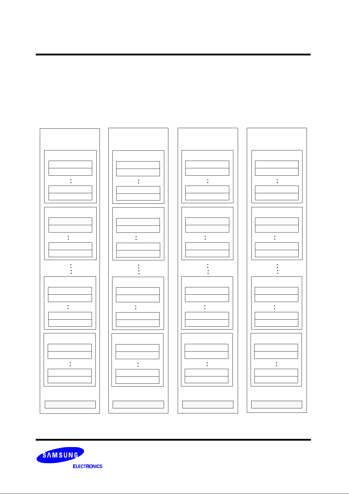
The device is arranged in four 128Mbit memory planes. Each plane contains 1,024 blocks and 528 byte(X8 device) or 264 word(X16
device) page registers. This allows it to perform simultaneous page program and block erase by selecting one page or block from
each plane. The block address map is configured so that multi-plane program/erase operations can be executed for every four
sequential blocks.
Plane 0
Plane 1
Plane 2
Plane 3
(1024 Block)
(1024 Block)
(1024 Block)
(1024 Block)
Page 0
Page 1
Page 31
Page 30
Memory Map
Block 0
Page 0
Page 1
Page 31
Page 30
Block 1
Page 0
Page 1
Page 31
Page 30
Block 2
Page 0
Page 1
Page 31
Page 30
Block 3
Page 0
Page 1
Page 31
Page 30
Block 4
Page 0
Page 1
Page 31
Page 30
Block 5
Page 0
Page 1
Page 31
Page 30
Block 6
Page 0
Page 1
Page 31
Page 30
Block 7
Page 0
Page 1
Page 31
Page 30
Block 4088
Page 0
Page 1
Page 31
Page 30
Block 4089
Page 0
Page 1
Page 31
Page 30
Block 4090
Page 0
Page 1
Page 31
Page 30
Block 4091
Page 0
Page 1
Page 31
Page 30
Block 4092
Page 0
Page 1
Page 31
Page 30
Block 4093
Page 0
Page 1
Page 31
Page 30
Block 4094
Page 0
Page 1
Page 31
Page 30
Block 4095
528byte Page Registers
Figure 3. Memory Array Map
528byte Page Registers 528byte Page Registers 528byte Page Registers
K9F1216U0A-YCB0,YIB0,PCB0,PIB0
FLASH MEMORY
12
K9F1216U0A-DCB0,DIB0,HCB0,HIB0
K9F1208U0A-YCB0,YIB0,PCB0,PIB0
K9F1208U0A-DCB0,DIB0,HCB0,HIB0
K9F1208Q0A-DCB0,DIB0,HCB0,HIB0 K9F1216Q0A-DCB0,DIB0,HCB0,HIB0
K9F1208U0A-VCB0,VIB0,FCB0,FIB0
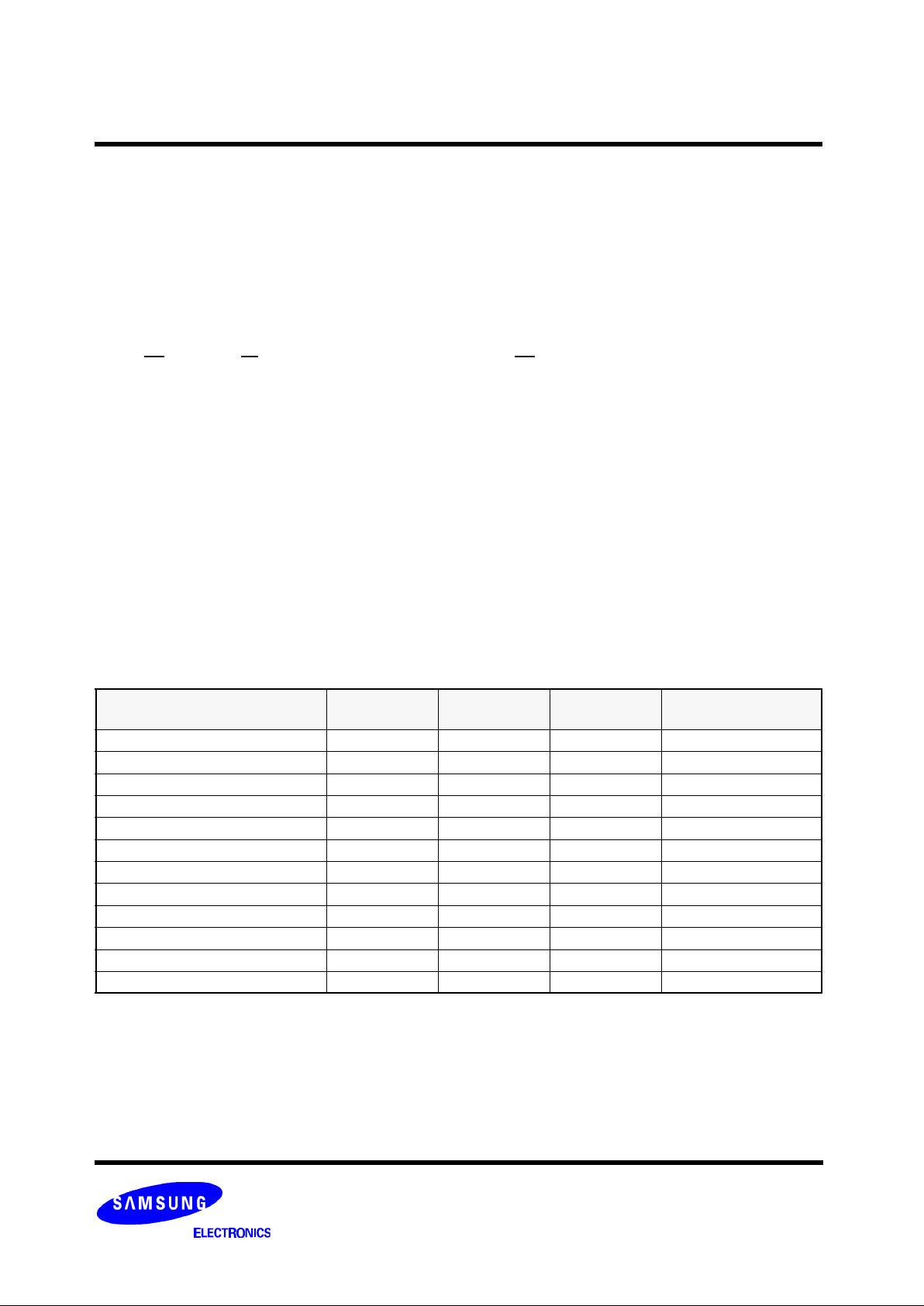
DC AND OPERATING CHARACTERISTICS(Recommended operating conditions otherwise noted.)
Parameter Symbol Test Conditions
K9F12XXQ0A(1.8V) K9F12XXU0A(3.3V) Unit
Min Typ Max Min Typ Max
Operat-
ing
Current
Sequential Read ICC1
tRC=50ns, CE=VIL
IOUT=0mA
- 8 15 - 10 20
mA
Program ICC2 - - 8 15 - 10 20
Erase ICC3 - - 8 15 - 10 20
Stand-by Current(TTL) ISB1 CE=VIH, WP=0V/VCC - - 1 - - 1
Stand-by Current(CMOS) ISB2 CE=VCC-0.2, WP=0V/VCC - 10 50 - 10 50
µA
Input Leakage Current ILI VIN=0 to Vcc(max) - - ±10 - - ±10
Output Leakage Current ILO VOUT=0 to Vcc(max) - - ±10 - - ±10
Input High Voltage VIH
I/O pins VCCQ-0.4 -
VCCQ
+0.3
2.0 - VCCQ+0.3
V
Except I/O pins VCC-0.4 -
VCC
+0.3
2.0 - VCC+0.3
Input Low Voltage, All inputs VIL - -0.3 - 0.4 -0.3 - 0.8
Output High Voltage Level VOH
K9F12XXQ0A :IOH=-100µA
K9F12XXU0A :IOH=-400µA
VCCQ-0.1 - - 2.4 - -
Output Low Voltage Level VOL
K9F12XXQ0A :IOL=100uA
K9F12XXU0A :IOL=2.1mA
- - 0.1 - - 0.4
Output Low Current(R/B) IOL(R/B)
K9F12XXQ0A :VOL=0.1V
K9F12XXU0A :VOL=0.4V
3 4 - 8 10 - mA
RECOMMENDED OPERATING CONDITIONS
(Voltage reference to GND, K9F12XXX0A-XCB0 :TA=0 to 70°C, K9F12XXX0A-XIB0:TA=-40 to 85°C)
Parameter Symbol
K9F12XXQ0A(1.8V)
K9F12XXU0A(3.3V)
Unit
Min Typ. Max Min Typ. Max
Supply Voltage VCC 1.70 1.8 1.95 2.7 3.3 3.6 V
Supply Voltage VCCQ 1.70 1.8 1.95 2.7 3.3 3.6 V
Supply Voltage VSS 0 0 0 0 0 0 V
ABSOLUTE MAXIMUM RATINGS
NOTE :
1. Minimum DC voltage is -0.6V on input/output pins. During transitions, this level may undershoot to -2.0V for periods <30ns.
Maximum DC voltage on input/output pins is VCC,+0.3V which, during transitions, may overshoot to VCC+2.0V for periods <20ns.
2. Permanent device damage may occur if ABSOLUTE MAXIMUM RATINGS are exceeded. Functional operation should be restricted to the conditions
as detailed in the operational sections of this data sheet. Exposure to absolute maximum rating conditions for extended periods may affect reliability.
Parameter Symbol
Rating
Unit
K9F12XXQ0A(1.8V) K9F12XXU0A(3.3V)
Voltage on any pin relative to VSS
VIN/OUT -0.6 to + 2.45 -0.6 to + 4.6
V
VCC -0.2 to + 2.45 -0.6 to + 4.6
VCCQ -0.2 to + 2.45 -0.6 to + 4.6
Temperature Under Bias
K9F12XXX0A-XCB0
TBIAS
-10 to +125
°C
K9F12XXX0A-XIB0 -40 to +125
Storage Temperature
K9F12XXX0A-XCB0
TSTG -65 to +150 °C
K9F12XXX0A-XIB0
Short Circuit Current Ios 5 mA
K9F1216U0A-YCB0,YIB0,PCB0,PIB0
FLASH MEMORY
13
K9F1216U0A-DCB0,DIB0,HCB0,HIB0
K9F1208U0A-YCB0,YIB0,PCB0,PIB0
K9F1208U0A-DCB0,DIB0,HCB0,HIB0
K9F1208Q0A-DCB0,DIB0,HCB0,HIB0 K9F1216Q0A-DCB0,DIB0,HCB0,HIB0
K9F1208U0A-VCB0,VIB0,FCB0,FIB0
CAPACITANCE(TA=25°C, VCC=1.8V/3.3V, f=1.0MHz)
NOTE : Capacitance is periodically sampled and not 100% tested.
Item Symbol Test Condition Min Max Unit
Input/Output Capacitance CI/O VIL=0V - 10 pF
Input Capacitance CIN VIN=0V - 10 pF
VALID BLOCK
NOTE :
1. The K9F12XXX0A may include invalid blocks when first shipped. Additional invalid blocks may develop while being used. The number of valid blocks
is presented with both cases of invalid blocks considered. Invalid blocks are defined as blocks that contain one or more bad bits. Do not erase or
program factory-marked bad blocks. Refer to the attached technical notes for a appropriate management of invalid blocks.
2. The 1st block, which is placed on 00h block address, is fully guaranteed to be a valid block, does not require Error Correction.
3. Minimum 1004 valid blocks are guaranteed for each contiguous 128Mb memory space.
Parameter Symbol Min Typ. Max Unit
Valid Block Number NVB 4,026 - 4,096 Blocks
AC TEST CONDITION
(K9F12XXX0A-XCB0 :TA=0 to 70°C, K9F12XXX0A-XIB0:TA=-40 to 85°C
K9F12XXQ0A : Vcc=1.70V~1.95V , K9F12XXU0A : Vcc=2.7V~3.6V unless otherwise noted)
Parameter K9F12XXQ0A K9F12XXU0A
Input Pulse Levels 0V to VccQ 0.4V to 2.4V
Input Rise and Fall Times 5ns 5ns
Input and Output Timing Levels VccQ/2 1.5V
K9F12XXQ0A:Output Load (VccQ:1.8V +/-10%)
K9F12XXU0A:Output Load (VccQ:3.0V +/-10%)
1 TTL GATE and CL=30pF 1 TTL GATE and CL=50pF
K9F12XXU0A:Output Load (VccQ:3.3V +/-10%) - 1 TTL GATE and CL=100pF
MODE SELECTION
NOTE : 1. X can be VIL or VIH.
2. WP should be biased to CMOS high or CMOS low for standby.
CLE ALE CE WE RE WP Mode
H L L H X
Read Mode
Command Input
L H L H X Address Input(4clock)
H L L H H
Write Mode
Command Input
L H L H H Address Input(4clock)
L L L H H Data Input
L L L H X Data Output
L L L H H X During Read(Busy) on K9F12XXX0A-Y,P or K9F1208U0A-V,F
X X X X H X
During Read(Busy) on the devices except K9F12XXX0A-Y,P and
K9F1208U0A-V,F
X X X X X H During Program(Busy)
X X X X X H During Erase(Busy)
X
X
(1)
X X X L Write Protect
X X H X X
0V/VCC
(2)
Stand-by
Program / Erase Characteristics
Parameter Symbol Min Typ Max Unit
Program Time tPROG - 200 500 µs
Dummy Busy Time for Multi Plane Program tDBSY 1 10
µs
Number of Partial Program Cycles
in the Same Page
Main Array
Nop
- - 1 cycle
Spare Array - - 2 cycles
Block Erase Time tBERS - 2 3 ms
 Loading...